EP0177129B1 - Verfahren zum Herstellen eines GaAs-Feldeffekttransistors - Google Patents
Verfahren zum Herstellen eines GaAs-Feldeffekttransistors Download PDFInfo
- Publication number
- EP0177129B1 EP0177129B1 EP85305237A EP85305237A EP0177129B1 EP 0177129 B1 EP0177129 B1 EP 0177129B1 EP 85305237 A EP85305237 A EP 85305237A EP 85305237 A EP85305237 A EP 85305237A EP 0177129 B1 EP0177129 B1 EP 0177129B1
- Authority
- EP
- European Patent Office
- Prior art keywords
- layer
- insulative
- conductive
- substrate
- gate
- Prior art date
- Legal status (The legal status is an assumption and is not a legal conclusion. Google has not performed a legal analysis and makes no representation as to the accuracy of the status listed.)
- Expired
Links
Images


Classifications
-
- H—ELECTRICITY
- H10—SEMICONDUCTOR DEVICES; ELECTRIC SOLID-STATE DEVICES NOT OTHERWISE PROVIDED FOR
- H10D—INORGANIC ELECTRIC SEMICONDUCTOR DEVICES
- H10D30/00—Field-effect transistors [FET]
- H10D30/01—Manufacture or treatment
- H10D30/061—Manufacture or treatment of FETs having Schottky gates
- H10D30/0612—Manufacture or treatment of FETs having Schottky gates of lateral single-gate Schottky FETs
- H10D30/0616—Manufacture or treatment of FETs having Schottky gates of lateral single-gate Schottky FETs using processes wherein the final gate is made before the completion of the source and drain regions, e.g. gate-first processes
-
- H—ELECTRICITY
- H10—SEMICONDUCTOR DEVICES; ELECTRIC SOLID-STATE DEVICES NOT OTHERWISE PROVIDED FOR
- H10D—INORGANIC ELECTRIC SEMICONDUCTOR DEVICES
- H10D30/00—Field-effect transistors [FET]
- H10D30/80—FETs having rectifying junction gate electrodes
- H10D30/87—FETs having Schottky gate electrodes, e.g. metal-semiconductor FETs [MESFET]
-
- H—ELECTRICITY
- H10—SEMICONDUCTOR DEVICES; ELECTRIC SOLID-STATE DEVICES NOT OTHERWISE PROVIDED FOR
- H10D—INORGANIC ELECTRIC SEMICONDUCTOR DEVICES
- H10D64/00—Electrodes of devices having potential barriers
- H10D64/01—Manufacture or treatment
- H10D64/012—Manufacture or treatment of electrodes comprising a Schottky barrier to a semiconductor
- H10D64/0124—Manufacture or treatment of electrodes comprising a Schottky barrier to a semiconductor to Group III-V semiconductors
- H10D64/0125—Manufacture or treatment of electrodes comprising a Schottky barrier to a semiconductor to Group III-V semiconductors characterised by the sectional shape, e.g. T or inverted T
-
- H—ELECTRICITY
- H10—SEMICONDUCTOR DEVICES; ELECTRIC SOLID-STATE DEVICES NOT OTHERWISE PROVIDED FOR
- H10D—INORGANIC ELECTRIC SEMICONDUCTOR DEVICES
- H10D64/00—Electrodes of devices having potential barriers
- H10D64/01—Manufacture or treatment
- H10D64/012—Manufacture or treatment of electrodes comprising a Schottky barrier to a semiconductor
- H10D64/0124—Manufacture or treatment of electrodes comprising a Schottky barrier to a semiconductor to Group III-V semiconductors
- H10D64/0125—Manufacture or treatment of electrodes comprising a Schottky barrier to a semiconductor to Group III-V semiconductors characterised by the sectional shape, e.g. T or inverted T
- H10D64/0126—Manufacture or treatment of electrodes comprising a Schottky barrier to a semiconductor to Group III-V semiconductors characterised by the sectional shape, e.g. T or inverted T the sectional shape being asymmetrical
-
- H—ELECTRICITY
- H10—SEMICONDUCTOR DEVICES; ELECTRIC SOLID-STATE DEVICES NOT OTHERWISE PROVIDED FOR
- H10D—INORGANIC ELECTRIC SEMICONDUCTOR DEVICES
- H10D64/00—Electrodes of devices having potential barriers
- H10D64/01—Manufacture or treatment
- H10D64/013—Manufacture or treatment of electrodes having a conductor capacitively coupled to a semiconductor by an insulator
- H10D64/01302—Manufacture or treatment of electrodes having a conductor capacitively coupled to a semiconductor by an insulator the insulator being formed after the semiconductor body, the semiconductor being silicon
- H10D64/01304—Manufacture or treatment of electrodes having a conductor capacitively coupled to a semiconductor by an insulator the insulator being formed after the semiconductor body, the semiconductor being silicon characterised by the conductor
- H10D64/01326—Aspects related to lithography, isolation or planarisation of the conductor
- H10D64/0133—Aspects related to lithography, isolation or planarisation of the conductor at least part of the entire electrode being a sidewall spacer, being formed by transformation under a mask or being formed by plating at a sidewall
-
- H—ELECTRICITY
- H10—SEMICONDUCTOR DEVICES; ELECTRIC SOLID-STATE DEVICES NOT OTHERWISE PROVIDED FOR
- H10P—GENERIC PROCESSES OR APPARATUS FOR THE MANUFACTURE OR TREATMENT OF DEVICES COVERED BY CLASS H10
- H10P76/00—Manufacture or treatment of masks on semiconductor bodies, e.g. by lithography or photolithography
- H10P76/40—Manufacture or treatment of masks on semiconductor bodies, e.g. by lithography or photolithography of masks comprising inorganic materials
- H10P76/408—Manufacture or treatment of masks on semiconductor bodies, e.g. by lithography or photolithography of masks comprising inorganic materials characterised by their sizes, orientations, dispositions, behaviours or shapes
- H10P76/4085—Manufacture or treatment of masks on semiconductor bodies, e.g. by lithography or photolithography of masks comprising inorganic materials characterised by their sizes, orientations, dispositions, behaviours or shapes characterised by the processes involved to create the masks
Definitions
- This invention relates to a field effect transistor and more particularly to a manufacturing method of a field effect transistor device whose substrate is prepared from gallium arsenide (GaAs) semiconductor material.
- GaAs gallium arsenide
- Field effect transistors prepared from gallium arsenide are widely accepted as semiconductor elements constituting important circuit elements involved in high frequency amplifiers and oscillators. Recently, IC devices comprised of GaAs FETs have assumed greater importance due to their various merits.
- the high frequency index Pf of a GaAs FET is expressed as where,
- the object of improving the high frequency property of the GaAs FET is attained by reducing the stray capacitance Cgs between the gate and source of the GaAs FET and/or increase the transconductance of the FET.
- the transconductance gm of the FET is further defined as: where,
- the improvement of the transconductance of the FET has to be attained by reducing the series resistance R s between the source and gate of the GaAs FET and/or enlarging the true transconductance gm0 itself. Enlargement of the true transconductance gm0 can be effected by shortening the gate.
- the foregoing discussion shows that it is necessary for the improvement of the high frequency property of the GaAs FET to reduce the series resistance R s between the source and gate of the GaAs FET and/or shorten the gate as much as possible.
- the gate-drain withstand voltage property as an important parameter in studying the performance of the GaAs FET.
- the drain voltage is set at 3 volts, and the pinch-off voltage is set at -2 volts. Then a maximum voltage of 5 volts is impressed on the gate-drain region of one FET gate.
- the breakdown voltage (rating) of the gate-drain region of the GaAs FET should be higher than at least 5 volts.
- the gate-drain breakdown voltage of the GaAs FET is demanded to be higher than 10 volts.
- a "recess structure” type device which is intended to minimize the series resistance R s between the source region and gate layer.
- the term "recess structure” is defined to mean a specific operational layer whose surface portion positioned under a gate electrode is etched and made thinner.
- the recess structure is still accompanied with the drawbacks that the fabrication of part of the aforementioned operational layer into a specific shape is difficult for the present day etching technique, and it is impossible to provide a recess structure bearing a satisfactory shape which allows for high shape controllability and high reproducibility.
- a method for manufacturing a GaAs field effect transistor characterized in that said method comprises the steps of:
- a method for manufacturing a GaAs field effect transistor characterized in that said method comprises the steps of:
- the source and drain regions are self-aligned with the gate structure.
- the source region is adjacent to the conductive portion.
- the drain region is spaced apart from the gate layer at a distance equal to the width of the insulative portion.
- a GaAs FET manufactured by the above-mentioned process offers the advantages that the width of the conductive portion can be reduced to a submicron extent easily (without applying any special fabricating technique) and the conductive portion is spaced from the drain region by a distance equal to the width of the insulative portion thereby improving the gate-drain breakdown voltage property of the GaAs FET.
- Figs. 1A to 1H are the enlarged cross sectional views of a GaAs field effect transistor (GaAs FET) according to a first embodiment of this invention, showing the main sequential steps of manufacturing said embodiments; and
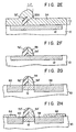
- Figs. 2A to 2H are the enlarged cross sectional views of a GaAs field effect transistor (GaAs FET) according to a second embodiment of the invention, showing the main sequential steps of manufacturing said embodiment.
- GaAs FET GaAs field effect transistor
- reference numeral 10 denotes a semiconductor gallium arsenide (GaAs) substrate doped with chromium (Cr).
- Si + ion is implanted into the surface of the substrate 10 by means of selective ion implantation to provide an N conductivity type impurity region 12.
- the selective implantation of Si + ion is carried out under the conditions of, for example, 100 KeV and 3.Ox10'2/cmz.
- the N conductivity type impurity region 12 functions as an operational layer of the FET.
- An insulative layer 14 prepared from Si0 2 is deposited on the substrate 10 by the chemical vapor deposition (CVD) method.
- the Si0 2 layer 14 is defined to have a thickness of about 1 micron.
- the insulative layer 14 is patterned so as to provide a mask layer whose side edge 14a lies at a specified position on the substrate 10.
- the insulative layer 14 covers that portion of the operational layer 12 where a drain region 24 is to be formed, and also defines the drain side edge of a gate metal layer 16 formed by the subsequent step.
- the Si0 2 layer 14 is etched by an anisotropic process, for example, by means of reactive ion etching (RIE) involving the application of a gaseous mixture of CF 4 and H 2 or a gas of CHF 3 .
- RIE reactive ion etching
- the side wall 14a of the insulative layer 14 is made substantially perpendicular to the substrate surface as seen from Fig. 1A.
- the reason is that the application of the RIE process causes the layer 14 to be etched with a strong anisotropic characteristic toward the thickness of the layer 14.
- a conductive layer 16 is deposited with a uniform thickness over the underlying layer expanse shown in Fig. 1A.
- This conductive layer 16 is prepared from tungsten silicide (WSi 2 ).
- This WSi 2 layer 16 was formed with a thickness of about 500 nm (5000 A) by the CVD process involving the application of a gaseous mixture of WF 6 and SiH 4 .
- This metal conductive layer 16 uniformly covers the substrate 10 and the insulative layer 14 formed on the substrate 10 with the aformentioned edge 14a. Consequently, the metal conductive layer 16 has an outline truthfully representing the stepped portion of the perpendicular edge 14a.
- the metal 16 is anisotropically grown in directions parallel with the surface of the substrate 10 as well as perpendicular to said surface. The reason is that the CVD process has an excellent property of securing covering of even a stepped portion. Therefore, the horizontal length 11 of the stepped portion of the metal layer 16 which is set adjacent to the side wall 14a of the insulative layer 14 was made substantially equal to the thickness t1 of the insulative layer 14 as shown in Fig. 1B.
- the mass of the superposed layers shown in Fig. 1B is anisotropically etched by the RIE process.
- the metal layer 16 is uniformly etched vertically to an extent equal to its thickness t1.
- the metal layer 16 is etched along its thickness with a strong anisotropic characteristic. Therefore, the etching does not substantially proceed in the lateral direction.
- a metal layer component 16' is retained in such a manner that it lies on part of the substrate surface and is set adjacent to the side wall 14a of the patterned insulative layer 14.
- the etching proceeds only in a direction extending from the upper surface of the metal layer 16 along its thickness, that is, a perpendicular direction.
- etching proceeds to an extent corresponding to the thickness (t1) of the metal layer 16 in the flat surface of the substrate 10, then the RIE process is completed. Consequently, a metal component 16' set adjacent to the side wall 14a of the insulative layer 14 is retained.
- This retained metal component 16' functions as the gate electrode of the GaAs FET.
- the retained metal component 16' has a width of about 0.5 micron substantially equal to the thickness t1 of the layer 14 deposited on the substrate 10. In other words, a gate electrode has been formed with a thickness reduced to an extent of submicrons.
- the metal component 16' (gate layer) alone is retained on the substrate 10.
- This metal component 16' comprises a side wall 16a truthfully representing the perpendicular side wall 14a of the Si0 2 layer 14 and a plane 16b inclined rightward to said side wall 16a.
- an Si0 2 layer 18 is deposited on the aformentioned mass of superposed layers by the plasma CVD process involving the application of a gaseous mixture of SiH 4 and N 2 0.
- the Si0 2 layer 18 has its thickness defined to be about 0.3 micron smaller than that of the aforesaid Si0 2 layer 14.
- the plasma CVD process applied in the deposition of the Si0 2 layer 18 has an excellent a property of covering a stepped portion as the aformentioned CVD process. Namely, the plasma CVD process can provide a cover truthfully representing the undulating outline of the underlying layer.
- the Si0 2 layer 18 deposited by the plasma CVD process is grown isotropically in a direction parallel with the surface of the substrate 10 as well as in a direction perpendicular to said surface. As shown in Fig. 1E, therefore, the lateral length of the Si0 2 insulative layer 18 set adjacent to the perpendicular wall of the gate electrode 16' is made substantially equal to the thickness t2 of said Si0 2 insulative layer 18.
- the RIE etching process involving the application of a gaseous mixture of CF 4 and H 2 is carried out.
- the. insulative Si0 2 layer 18 is vertically etched to a uniform extent equal to the thickness t2 of the insulative layer 16.
- the etching of the insulative Si0 2 layer 18 proceeds with a very strong isotropical property along the thickness of the insulative Si0 2 layer 18.
- an Si0 2 layer component 18' is retained on the substrate 10 so as to be set adjacent to the side wall 16a of the gate electrode layer 16'.
- the retained Si0 2 layer component 18' has a thickness of about 0.3 micron substantially equal to that t2 of the previously deposited Si0 2 layer 18.
- a projection 20 is provided on the active layer 12 of the substrate 10 which is constructed by the joint vertical abutment of the gate metal layer 16' and insulative layer 18'.
- This projecting abutted mass 20 has a width of 0.8 micron, because the gate metal layer 16' has a width of 0.5 micron and the insulative Si0 2 layer component 18' has a width of 0.3 micron.
- Si + ion is implanted in the structure of Fig. 1 F by masking the areas other than the operational layer 12 (constituting the source and drain regions) of the FET with a photoresist film (not shown).
- the implantation of the Si+ ion was carried out under the conditions of, for example, 150 KeV and 3.0 ⁇ 10 13 /cm 2 .
- the projecting abutted mass 20 acts as a mask, thereby preventing ions from being implanted in the layers 12 underlying the projecting abutted mass 20. Consequently, as shown in Fig.
- n + layers 22 22, 24 highly concentrated impurity implanted layers (n + layers) 22, 24 are formed while effecting self-alignment with the projecting abutted mass 20.
- the n + layers 22, 24 which are formed with a greater depth than the active layer 12 serve as the source and drain regions of the GaAs FET.
- the source region 22 is drawn near the gate metal layer 16', whereas the drain layer 24 is removed from the gate layer 16' to an extent equal to the width of the insulative layer 18'. In other words, the gate layer 16' takes an offset position with respect to the drain regions 24.
- the wafer of Fig. 1G in which the source and drain regions are formed by ion implantation is subsequently annealed to activate the impurity ions implanted into the substrate 10.
- the annealing was applied at a temperature of 850°C for 10 minutes.
- highly conductive metal layers 26, 28 are respectively deposited on the source and drain regions 22, 24 to function as source and drain electrodes.
- These electrodes 26, 28 are prepared from AuGe base alloy, and are set apart from the projection abutted mass 20 consisting of the gate metal layer 16 and insulative layer 18' at a prescribed distance.
- the GaAs FET is completed through the above-mentioned steps.
- the gate has a length reduced to the submicron extent (0.5 micron in the example).
- the source is set adjacent to the gate, thereby prominently minimizing a series resistance R s between the source and gate regions. Consequently, the transconductance gm of the GaAs FET is increased, to improve the high frequency property of this element.
- still imperfect manufacturing processes such as electron beam irradiation or X-ray lithography is not applied at all to provide a gate having a length of the submicron order. Namely, this invention can provide a fine gate under well-controlled conditions simply by applying a process widely accepted at present. This fact bears great industrial importance for the GaAs FET manufactures in general, because they can be produced at low cost.
- the GaAs FET of this invention is improved not only in its high frequency property, but also in its gate-drain breakdown voltage property.
- the reason is that the drain layer 24 is removed from the gate layer 16' to an extent equal to the width (0.3 micron) of the insulative layer 18' which is in contact with the gate layer 16' having a width of 0.5 micron.
- the offset position of the gate element has elevated the gate-drain breakdown voltage property by about 12 volts.
- This value means that the gate-drain breakdown voltage of the GaAs FET of the present invention has been improved to be about twice that of the conventional device.
- the method of this invention enables a GaAs FET device which excels in both its high frequency and gate-drain withstand voltage properties to be effectively manufactured and at less cost within present day fabrication techniques.
- Figs. 2A to 2H of the method of manufacturing a GaAs FET according to a second embodiment of this invention.
- the parts of Figs. 2A to 2H the same as those of the GaAs FET of Fig. 1 are denoted by the same numerals, detailed description thereof being omitted.
- N conductivity type impurity region 12 functioning as the operational layer of the GaAs FET is formed on the surface of a GaAs substrate 10 by a selective ion-implantation process.
- amorphous silicon layer 50 (functioning as a spacer film) with a thickness of 0.5 micron.
- the amorphous silicon layer 50 is patterned by the RIE etching process.
- the silicon layer 50 is provided with an edge 50a set perpendicular at a prescribed position on the substrate 10.
- the silicon layer 50 covers a source region formed in the aforesaid layer 12.
- the perpendicular edge 50a defines the drain side of a subsequently deposited gate 54.
- An Si0 2 layer 52 is deposited on the underlying mass of superposed layers with a uniform thickness T1 (ex. 0.3 micron) by the CVD process.
- the Si0 2 layer 52 covers the substrate 10 and the amorphous silicon layer 50 having a perpendicular edge 50a with a uniform thickness.
- the horizontal length L1 of that portion of the Si0 2 layer 52 which is set adjacent to the side wall 50a of the silicon layer 50 is made substantially equal to the thickness T1 of the layer 50. This feature is derived from the excellent stepped portion-covering property of the CVD method as previously described with respect to the first embodiment.
- the Si0 2 layer 52 is anisotropically etched in the vertical direction by the RIE etching process uniformly to an extent equal to the thickness T1 of the Si0 2 layer 52.
- a Si0 2 layer component 52' is retained on the substrate 10 so as to be in lateral contact with the side wall 50a of the patterned silicon layer 50.
- the etching process applied in the second embodiment is characterized in that when the Si0 2 layer 52 is etched by the RIE etching process, the etching proceeds from the upper surface of said layer 52 only along the thickness thereof (that is, in the vertical direction), and the RIE etching process is completed when etching proceeds to an extent equal to the thickness T1 of the layer 52 on the surface of the substrate 10.
- an insulator component 52' is retained on the substrate 10 so as to be in contact with the side wall 50a of the silicon layer 50.
- This retained insulator component 52' has a thickness of about 0.3 micron substantially equal to that T1 of the insulative layer 14 deposited on the substrate 10.
- the insulator component 52' alone (Fig. 2D) is retained on the substrate 10.
- This insulator component 52' comprises a side wall 52a truthfully representing the perpendicular side wall 50a of the silica layer 50 and an inclined plane 52b provided on the opposite side to said perpendicular side wall 50a.
- a metal layer 54 is uniformly deposited on the underlying structure of superposed layers of Fig. 2D.
- the gate metal is prepared from tungsten silicide WSi 2 .
- the metal layer 54 is defined to have a thickness T2 of, for example, 0.5 micron.
- the CVD method having an excellent stepped portion-covering property enables the metal layer 54 to be isotropically grown in a direction parallel with the surface of the substrate 10 and also in a direction perpendicular to the substrate surface. As shown in Fig. 2E, therefore, that portion of the metal layer 54 which is set adjacent to the perpendicular side wall 52a of the retained insulator component 52' has a length L2 substantially equal to the thickness T2 of the metal layer 54.
- the metal 54 is uniformly etched in a vertical direction by the RIE process to an extent equal to its thickness T2.
- a metal layer component 54' is retained on the substrate 10 so as to be set adjacent to the side wall of the aforesaid insulative layer 52 (Fig. 2F).
- a projecting abutted mass 56 consisting of the layer components 52', 54'.
- the layer component 54' serves as the gate electrode of the GaAs FET, and has a width of about 0.5 micron substantially equal to that T2 of the deposited metal layer 54.
- Source and drain regions 58, 60 are formed by ion implantation so as to be self-aligned with a projecting abutted layer 56 consisting of a gate layer 54' and insulator 52', and later are annealed (Fig. 2G), thereby providing source and drain electrodes 62,64 (Fig. 2H).
- Fig. 2G a projecting abutted layer 56 consisting of a gate layer 54' and insulator 52'
- Fig. 2G annealed
- the gate layer 54' is removed from the drain layer 60 at a distance equal to the width of the insulator 52'.
- the manufacturing method of the second embodiment of this invention enables a GaAs FET with excellent high frequency and gate-drain breakdown voltage properties to be manufactured effectively and at low cost within the range of present day fabrication techniques.
- the materials, the conditions for defining the parameters of the CVD and RIE processes and the annealing conditions are not limited to those already described, but may be varied as the need arises.
- the spacer film 50 which is deposited on the substrate 10 to define the perpendicular side wall 50a of the insulator component 52', is made of amorphous silicon.
- other materials may be used for the spacer film 50, if they can be effectively etched off without damaging the insulator component 52'.
Landscapes
- Junction Field-Effect Transistors (AREA)
- Drying Of Semiconductors (AREA)
Claims (10)
Applications Claiming Priority (2)
| Application Number | Priority Date | Filing Date | Title |
|---|---|---|---|
| JP59204416A JPS6182482A (ja) | 1984-09-29 | 1984-09-29 | GaAs電界効果トランジスタの製造方法 |
| JP204416/84 | 1984-09-29 |
Publications (2)
| Publication Number | Publication Date |
|---|---|
| EP0177129A1 EP0177129A1 (de) | 1986-04-09 |
| EP0177129B1 true EP0177129B1 (de) | 1989-04-05 |
Family
ID=16490177
Family Applications (1)
| Application Number | Title | Priority Date | Filing Date |
|---|---|---|---|
| EP85305237A Expired EP0177129B1 (de) | 1984-09-29 | 1985-07-23 | Verfahren zum Herstellen eines GaAs-Feldeffekttransistors |
Country Status (4)
| Country | Link |
|---|---|
| US (1) | US4645563A (de) |
| EP (1) | EP0177129B1 (de) |
| JP (1) | JPS6182482A (de) |
| DE (1) | DE3569313D1 (de) |
Families Citing this family (26)
| Publication number | Priority date | Publication date | Assignee | Title |
|---|---|---|---|---|
| US4743565A (en) * | 1981-03-30 | 1988-05-10 | International Business Machines Corporation | Lateral device structures using self-aligned fabrication techniques |
| JPS60137070A (ja) * | 1983-12-26 | 1985-07-20 | Toshiba Corp | 半導体装置の製造方法 |
| US4956308A (en) * | 1987-01-20 | 1990-09-11 | Itt Corporation | Method of making self-aligned field-effect transistor |
| DE3602461A1 (de) * | 1986-01-28 | 1987-07-30 | Telefunken Electronic Gmbh | Verfahren zum herstellen eines sperrschicht-feldeffekttransistors |
| US4689869A (en) * | 1986-04-07 | 1987-09-01 | International Business Machines Corporation | Fabrication of insulated gate gallium arsenide FET with self-aligned source/drain and submicron channel length |
| US4735681A (en) * | 1986-08-15 | 1988-04-05 | Motorola Inc. | Fabrication method for sub-micron trench |
| FR2618011B1 (fr) * | 1987-07-10 | 1992-09-18 | Commissariat Energie Atomique | Procede de fabrication d'une cellule de memoire |
| KR920009718B1 (ko) * | 1987-08-10 | 1992-10-22 | 스미도모덴기고오교오 가부시기가이샤 | 화합물반도체장치 및 그 제조방법 |
| JP2685149B2 (ja) * | 1988-04-11 | 1997-12-03 | 住友電気工業株式会社 | 電界効果トランジスタの製造方法 |
| JPH0748503B2 (ja) * | 1988-11-29 | 1995-05-24 | 三菱電機株式会社 | 電界効果トランジスタの製造方法 |
| JPH02253632A (ja) * | 1989-03-27 | 1990-10-12 | Matsushita Electric Ind Co Ltd | 電界効果型トランジスタの製造方法 |
| JP2553699B2 (ja) * | 1989-04-12 | 1996-11-13 | 三菱電機株式会社 | 半導体装置の製造方法 |
| US5250453A (en) * | 1989-04-12 | 1993-10-05 | Mitsubishi Denki Kabushiki Kaisha | Production method of a semiconductor device |
| EP0416141A1 (de) * | 1989-09-04 | 1991-03-13 | Siemens Aktiengesellschaft | Verfahren zur Herstellung eines FET mit asymmetrisch angeordnetem Gate-Bereich |
| JPH0817184B2 (ja) * | 1989-11-08 | 1996-02-21 | 三菱電機株式会社 | 化合物半導体装置の製造方法 |
| JP2786307B2 (ja) * | 1990-04-19 | 1998-08-13 | 三菱電機株式会社 | 電界効果トランジスタ及びその製造方法 |
| JPH0475351A (ja) * | 1990-07-17 | 1992-03-10 | Mitsubishi Electric Corp | 化合物半導体装置の製造方法 |
| US5110760A (en) * | 1990-09-28 | 1992-05-05 | The United States Of America As Represented By The Secretary Of The Navy | Method of nanometer lithography |
| JPH0591848A (ja) * | 1991-09-30 | 1993-04-16 | Mamegen:Kk | 苦汁100%による絹ごし豆腐の製造方法 |
| US5304511A (en) * | 1992-09-29 | 1994-04-19 | Mitsubishi Denki Kabushiki Kaisha | Production method of T-shaped gate electrode in semiconductor device |
| US5773334A (en) * | 1994-09-26 | 1998-06-30 | Toyota Jidosha Kabushiki Kaisha | Method of manufacturing a semiconductor device |
| US5994728A (en) * | 1995-11-15 | 1999-11-30 | Matsushita Electronics Corporation | Field effect transistor and method for producing the same |
| KR19980078235A (ko) * | 1997-04-25 | 1998-11-16 | 문정환 | 반도체 소자의 제조 방법 |
| DE10101825B4 (de) | 2001-01-17 | 2006-12-14 | United Monolithic Semiconductors Gmbh | Verfahren zur Herstellung eines Halbleiter-Bauelements mit einer T-förmigen Kontaktelektrode |
| KR20040056839A (ko) * | 2002-12-24 | 2004-07-01 | 아남반도체 주식회사 | 반도체 소자 제조 방법 |
| US20060046229A1 (en) * | 2004-08-26 | 2006-03-02 | Teich Thomas J | Dental implant |
Family Cites Families (5)
| Publication number | Priority date | Publication date | Assignee | Title |
|---|---|---|---|---|
| US4378627A (en) * | 1980-07-08 | 1983-04-05 | International Business Machines Corporation | Self-aligned metal process for field effect transistor integrated circuits using polycrystalline silicon gate electrodes |
| US4400865A (en) * | 1980-07-08 | 1983-08-30 | International Business Machines Corporation | Self-aligned metal process for integrated circuit metallization |
| US4455738A (en) * | 1981-12-24 | 1984-06-26 | Texas Instruments Incorporated | Self-aligned gate method for making MESFET semiconductor |
| JPS59114871A (ja) * | 1982-12-21 | 1984-07-03 | Toshiba Corp | シヨツトキ−ゲ−ト型GaAs電界効果トランジスタの製造方法 |
| JPS59124172A (ja) * | 1982-12-30 | 1984-07-18 | インタ−ナシヨナル ビジネス マシ−ンズ コ−ポレ−シヨン | Fet製造方法 |
-
1984
- 1984-09-29 JP JP59204416A patent/JPS6182482A/ja active Pending
-
1985
- 1985-07-17 US US06/755,799 patent/US4645563A/en not_active Expired - Lifetime
- 1985-07-23 DE DE8585305237T patent/DE3569313D1/de not_active Expired
- 1985-07-23 EP EP85305237A patent/EP0177129B1/de not_active Expired
Also Published As
| Publication number | Publication date |
|---|---|
| EP0177129A1 (de) | 1986-04-09 |
| JPS6182482A (ja) | 1986-04-26 |
| DE3569313D1 (en) | 1989-05-11 |
| US4645563A (en) | 1987-02-24 |
Similar Documents
| Publication | Publication Date | Title |
|---|---|---|
| US4645563A (en) | Method of manufacturing GaAs field effect transistor | |
| US4711858A (en) | Method of fabricating a self-aligned metal-semiconductor FET having an insulator spacer | |
| US5036017A (en) | Method of making asymmetrical field effect transistor | |
| KR920002090B1 (ko) | 전계효과 트랜지스터의 제조방법 | |
| US4173818A (en) | Method for fabricating transistor structures having very short effective channels | |
| US6215152B1 (en) | MOSFET having self-aligned gate and buried shield and method of making same | |
| US4963501A (en) | Method of fabricating semiconductor devices with sub-micron linewidths | |
| US4149307A (en) | Process for fabricating insulated-gate field-effect transistors with self-aligned contacts | |
| US5950083A (en) | Method for fabricating CMOS transistor with self-aligned silicide (salicide) structure | |
| EP0083785A2 (de) | Verfahren zur Herstellung von selbstalignierten Feldeffekttransistoren für integrierte Schaltungen | |
| EP0113161B1 (de) | Verfahren zur Herstellung eines Feldeffekttransistors mit Schottky-Gate | |
| US4728621A (en) | Fabricating a field effect transistor utilizing a dummy gate | |
| US5770506A (en) | Method of fabricating a field effect transistor with short gate length | |
| US4997779A (en) | Method of making asymmetrical gate field effect transistor | |
| US5112766A (en) | Method of manufacturing field effect transistors | |
| US5001077A (en) | Method of producing an asymmetrically doped LDD MESFET | |
| US5550065A (en) | Method of fabricating self-aligned FET structure having a high temperature stable T-shaped Schottky gate contact | |
| US5043294A (en) | Method for manufacturing an FET with asymmetrical gate region | |
| US5484743A (en) | Self-aligned anti-punchthrough implantation process | |
| GB2230899A (en) | Method of producing a gate | |
| US4640000A (en) | Method of manufacturing semiconductor device | |
| JPH04305978A (ja) | 電力用mos半導体デバイスの製造方法 | |
| US5449628A (en) | Method of making semiconductor device having a short gate length | |
| US5640029A (en) | Field-effect transistor and method of producing same | |
| JP2888993B2 (ja) | 電界効果トランジスタの製造方法 |
Legal Events
| Date | Code | Title | Description |
|---|---|---|---|
| PUAI | Public reference made under article 153(3) epc to a published international application that has entered the european phase |
Free format text: ORIGINAL CODE: 0009012 |
|
| 17P | Request for examination filed |
Effective date: 19850805 |
|
| AK | Designated contracting states |
Kind code of ref document: A1 Designated state(s): DE FR GB SE |
|
| 17Q | First examination report despatched |
Effective date: 19871228 |
|
| GRAA | (expected) grant |
Free format text: ORIGINAL CODE: 0009210 |
|
| AK | Designated contracting states |
Kind code of ref document: B1 Designated state(s): DE FR GB |
|
| REF | Corresponds to: |
Ref document number: 3569313 Country of ref document: DE Date of ref document: 19890511 |
|
| ET | Fr: translation filed | ||
| PLBE | No opposition filed within time limit |
Free format text: ORIGINAL CODE: 0009261 |
|
| STAA | Information on the status of an ep patent application or granted ep patent |
Free format text: STATUS: NO OPPOSITION FILED WITHIN TIME LIMIT |
|
| 26N | No opposition filed | ||
| PGFP | Annual fee paid to national office [announced via postgrant information from national office to epo] |
Ref country code: FR Payment date: 19970709 Year of fee payment: 13 |
|
| PGFP | Annual fee paid to national office [announced via postgrant information from national office to epo] |
Ref country code: DE Payment date: 19970801 Year of fee payment: 13 |
|
| REG | Reference to a national code |
Ref country code: GB Ref legal event code: 746 Effective date: 19981015 |
|
| PG25 | Lapsed in a contracting state [announced via postgrant information from national office to epo] |
Ref country code: FR Free format text: LAPSE BECAUSE OF NON-PAYMENT OF DUE FEES Effective date: 19990331 |
|
| PG25 | Lapsed in a contracting state [announced via postgrant information from national office to epo] |
Ref country code: DE Free format text: LAPSE BECAUSE OF NON-PAYMENT OF DUE FEES Effective date: 19990501 |
|
| REG | Reference to a national code |
Ref country code: FR Ref legal event code: ST |
|
| REG | Reference to a national code |
Ref country code: GB Ref legal event code: IF02 |
|
| PGFP | Annual fee paid to national office [announced via postgrant information from national office to epo] |
Ref country code: GB Payment date: 20040721 Year of fee payment: 20 |
|
| PG25 | Lapsed in a contracting state [announced via postgrant information from national office to epo] |
Ref country code: GB Free format text: LAPSE BECAUSE OF EXPIRATION OF PROTECTION Effective date: 20050722 |
|
| REG | Reference to a national code |
Ref country code: GB Ref legal event code: PE20 |