EP0177285B1 - Adaptives Filtersystem - Google Patents
Adaptives Filtersystem Download PDFInfo
- Publication number
- EP0177285B1 EP0177285B1 EP85306872A EP85306872A EP0177285B1 EP 0177285 B1 EP0177285 B1 EP 0177285B1 EP 85306872 A EP85306872 A EP 85306872A EP 85306872 A EP85306872 A EP 85306872A EP 0177285 B1 EP0177285 B1 EP 0177285B1
- Authority
- EP
- European Patent Office
- Prior art keywords
- signal
- filter
- samples
- chrominance
- signal components
- Prior art date
- Legal status (The legal status is an assumption and is not a legal conclusion. Google has not performed a legal analysis and makes no representation as to the accuracy of the status listed.)
- Expired - Lifetime
Links
- 238000001914 filtration Methods 0.000 title claims abstract description 13
- 230000003044 adaptive effect Effects 0.000 title abstract description 11
- 239000002131 composite material Substances 0.000 claims abstract description 18
- 230000002829 reductive effect Effects 0.000 claims abstract description 4
- 230000001419 dependent effect Effects 0.000 claims abstract 5
- 230000007717 exclusion Effects 0.000 claims 6
- 238000001228 spectrum Methods 0.000 description 6
- 230000002238 attenuated effect Effects 0.000 description 3
- 239000003086 colorant Substances 0.000 description 2
- 230000000295 complement effect Effects 0.000 description 2
- 230000003111 delayed effect Effects 0.000 description 2
- 238000010586 diagram Methods 0.000 description 2
- 239000000203 mixture Substances 0.000 description 2
- 238000013459 approach Methods 0.000 description 1
- 230000001010 compromised effect Effects 0.000 description 1
- 230000001143 conditioned effect Effects 0.000 description 1
- 230000003247 decreasing effect Effects 0.000 description 1
- 230000001934 delay Effects 0.000 description 1
- 238000001514 detection method Methods 0.000 description 1
- 230000001771 impaired effect Effects 0.000 description 1
- 230000002452 interceptive effect Effects 0.000 description 1
- 238000000034 method Methods 0.000 description 1
- 239000011148 porous material Substances 0.000 description 1
- 238000005070 sampling Methods 0.000 description 1
- 229920006395 saturated elastomer Polymers 0.000 description 1
Images


Classifications
-
- H—ELECTRICITY
- H03—ELECTRONIC CIRCUITRY
- H03H—IMPEDANCE NETWORKS, e.g. RESONANT CIRCUITS; RESONATORS
- H03H19/00—Networks using time-varying elements, e.g. N-path filters
-
- H—ELECTRICITY
- H03—ELECTRONIC CIRCUITRY
- H03H—IMPEDANCE NETWORKS, e.g. RESONANT CIRCUITS; RESONATORS
- H03H21/00—Adaptive networks
- H03H21/0012—Digital adaptive filters
-
- H—ELECTRICITY
- H04—ELECTRIC COMMUNICATION TECHNIQUE
- H04N—PICTORIAL COMMUNICATION, e.g. TELEVISION
- H04N9/00—Details of colour television systems
- H04N9/64—Circuits for processing colour signals
- H04N9/646—Circuits for processing colour signals for image enhancement, e.g. vertical detail restoration, cross-colour elimination, contour correction, chrominance trapping filters
Definitions
- the present invention relates generally to electronic signal processing filters and particularly to filters having variable bandwidth frequency characteristics.
- Electronic signal processing filters may be used to remove the noise components from an information signal, to separate the low and high frequency components of a composite signal, or generally to recover the information contained in one frequency band of a signal without interference from components in other frequency bands.
- the NTSC composite video signal is an example of a signal having component signals with overlapping frequency spectra.
- the luminance and chrominance components of an NTSC composite video signal are disposed in a frequency interleaved relation.
- the luminance components are generally at integral multiples of a horizontal line scanning frequency (f h ) and chrominance components at odd multiples of one-half of the line scanning frequency (Mh).
- the luminance components occupy a frequency spectrum which ranges from 0 Hz to approximately 4.2 MHz and the chrominance components occupy a band of frequencies ranging from approximately 2.4 MHz to 4.2 MHz.
- Comb filter arrangements which separate the frequency interleaved luminance and chrominance components of the video signal. Where a comb filter is employed, however, reproduction of a color image tends to be impaired in the presence of relatively low frequency luminance signal components in the combed chrominance signal. These luminance signals, which, for example, may be produced for an image containing diagonal lines, reduce the vertical resolution and distort the colors of the reproduced image.
- conventional television receivers apply the combed chrominance signal to a low pass filter which may, for example, have a pass band from 0 to 1 MHz.
- the signal provided by this filter is added to the combed luminance signal and subtracted from the combed chrominance signal. This process restores the low frequency components to the luminance signals, increasing the vertical resolution of the image, and removes the contaminating components from the chrominance signals, reducing the color distortion.
- the luminance signals have a broad frequency spectrum it is desirable to recover as much of the luminance signal as possible from the combed chrominance signals. Accordingly, it is desirable to use a wide bandwidth low pass filter to recover the vertical detail information. When this is done, however, spurious dots may appear in the areas of the image which contain relatively saturated colors. These dots are cross-color interference produced by chrominance signals that have sufficient amplitude to pass through the low pass filter. Consequently, vertical detail low pass filters for color television receivers generally are designed to have a compromised bandwidth, providing as much increased vertical resolution as can be achieved without introducing cross-color interference.
- the embodiment of the invention described below is an adaptive low pass filter which has a pass band that becomes wider or narrower respectively in response to decreased or increased levels of chrominance in the input signals.
- an adaptive filter apparatus of that general form is characterized in that the signal splitter, which is coupled to the output port of the first filter, produces two output signals which are mutually inversely scaled replicas of the signal provided by the first filter.
- the splitter has a control signal input for changing the relative amplitude levels of the signals at its two output ports.
- the second filter is coupled to one of these output ports to reduce the bandwidth of the signal provided thereby.
- the signal combiner is coupled to the other one of the output ports of the signal splitter and to the output port of the second filter. It combines the signals provided by these devices to produce the output signal of the filtering system.
- the frequency characteristic of this filtering system has a pass-band which may vary in width between the bandwidth of the first filter and the bandwidth of the cascade combination of the first and second filters.
- the bandwidth of the filter system varies as a function of the control signal applied to the signal splitter.
- broad arrows represent busses for multiple-bit parallel digital signals. These busses carry eight-bit signals unless otherwise indicated by a slash across the bus and an adjacent number. Line arrows represent connections carrying analog signals or single-bit digital signals. A small circle at the input terminal of a logic element indicates that the element responds to the logical complement of that input signal.
- digital samples representing composite video signals are provided to comb filter 12 by a source of composite video signals 10.
- Source 10 may be, for example, the analog-to-digital (A/D) converter of a conventional digital television receiver.
- Comb filter 12 provides a digital combed luminance signal at its output port Y and a digital combed chrominance signal at its output port C.
- the chrominance signal is composed of two quadrature phase related color difference signals, I and Q.
- the samples are provided by the A/D converter at a rate equal to four times the color subcarrier frequency (4f sc ) the chrominance signal provided by the comb filter may be represented as alternating samples of these color difference signals (i.e.
- Samples from low pass filter 14 are applied to delay element 48.
- the delayed samples from delay element 48 are applied as the multiplicand input signal to sample scaler 49.
- the multiplier input signal to scaler 49 is an attenuating factor provided by multiplexer 45.
- Sample scaler 49 which may be, for example, a conventional 16 bit digital multiplier such as the AM29516 manufactured by Advanced Micro Devices, Inc., Sunnyvale, California, USA, provides samples that are attenuated replicas of the samples applied to its multiplicand input port.
- Delay element 48 provides compensating delay for the multiplicand samples from filter 14 while the value of the attenuation factor for the samples is determined.
- Attenuation network 40 which includes delay element 48, sample scaler 49, and the circuitry to generate the attenuation factors, is described in detail below.
- the samples provided by sample scaler 49 are applied to low pass filter 22.
- filter 22 is identical to low pass filter 14.
- the samples that are available at the output terminal of filter 22 have the frequency spectrum of signals that have been filtered by the cascade combination of filters 14 and 22.
- both filters 14 and 22 have frequency characteristics similar to curve 300 of FIGURE 3, it can be shown that the cascade combination of filters 14 and 22 has a frequency characteristic similar to curve 302. It is noted that the bandwidth of the characteristic represented by curve 302 is approximately 1 MHz and that signals having frequencies greater than 2.4 MHz are attenuated by more than 24 dB.
- the signals passed by the combination of filters 14 and 22, therefore, have less vertical detail information and less chrominance interference than the signals provided by filter 14 alone.
- Samples from low-pass filter 14 via delay element 18 are applied to the minuend input port, and samples from sample scaler 49 are applied to the subtrahend input port of subtracter 20.
- Subtracter 20 and sample scaler 49 constitute signal splitting circuitry that provides samples which are mutually supplementary at respective first and second output terminals 21,21'.
- the samples provided by filter 14 are represented by X and the samples provided by sample scaler 49 are represented by aX, a being the attenuation factor, then the samples available at the output of subtracter 20 may be represented as (1-a)X.
- the time delay provided by delay element 18 compensates for the processing time through delay element 48 and sample scaler 49.
- the samples provided by subtracter 20 are delayed by delay element 24 and applied to an input port of adder 26.
- Delay element 24 provides compensating delay equal to the processing delay through low pass filter 22.
- Samples from low-pass filter 22 are applied to the other input port of adder 26.
- Adder 26 produces samples representing the sum of a doubly filtered and attenuated signal and its singly filtered supplementary signal.
- the proportion of singly filtered signal to doubly filtered signal is determined by the level of attenuation applied by sample scaler 49.
- network 40 that controls the bandwidth of the filtering system.
- low pass filtered combed chrominance samples from filter 14 are applied to the subtrahend input port of subtracter 41 and unfiltered combed chrominance signals, from comb filter 12 are applied to the minuend input via delay element 16.
- Delay element 16 delays the combed chrominance samples by an amount of time equal to the processing time of filter 14.
- Subtracter 41 removes the low frequency components from the combed chrominance signals and effectively provides high pass filtered chrominance signals to I-Q demodulator 42.
- Demodulator 42 may be a conventional color difference signal demodulator such as the one described in U.S. Patent No.
- This demodulator may include a demultiplexer for separating the 4f sc combed chrominance samples into separate sequences of I and Q color difference signal samples that have a 2f sc rate (i.e. changing the sequence + I, + Q, -I, -Q, + I...into the two sequences + I, -I, + I...and +Q, -Q, +Q).
- the demodulator may include further circuitry to remove the color carrier from the I and Q sequences.
- the samples provided by the demodulator therefore, represent baseband I and Q color difference signals.
- the I and Q samples from demodulator 42 are applied to absolute value circuits 43 and 44 respectively which pass samples representing the magnitudes of the I and Q samples to the two data inputs of multiplexer 45.
- I signal magnitude samples from absolute value circuit 43 are applied to the minuend input port, and Q signal magnitude samples from absolute value circuit 44 are applied to the subtrahend input pore of subtracter 46.
- the sign bit output signal of subtracter 46 is in a logic high state (i.e. indicating a negative result) when the Q sample has a greater magnitude than the I sample and is in a logic low state otherwise.
- This signal controls multiplexer 45 to pass the four most significant bits of the greater of the two samples applied to its input ports. These four-bit samples are the attenuation factors that are applied to the multiplier input port of sample scaler 49.
- a low-pass filter may be inserted between the multiplexer 45 and the sample scaler 49.
- a filtering system which includes a filter of this type may be preferred when signals having a low signal to noise ratio are to be filtered.
- sample scaler 49 is a 16 bit parallel multiplier.
- the eight-bit samples from delay element 48 are applied as the eight most significant bits of the multiplicand input signal and the four bit samples from multiplexer 45 are applied as the four more significant bits of the eight least significant bits of the multiplier input signal.
- the output samples are available on lines 8 through 15 of the output bus where the lines that make up the output bus are numbered from 0 (least significant) to 31 (most significant).
- the four bits applied to the multiplier input port of the sample scaler 49 may represent the values 0 through 15/16.
- the correspondence between the amplitude of the chrominance samples and the value of the attenuation factor is shown in FIGURE 2.
- the horizontal axis represents the amplitude of the chrominance samples increasing from left to right. This axis is divided into sixteen parts, the leftmost part corresponding to chrominance magnitudes for which the four most significant bits, exclusive of the sign bit, are zeros and the rightmost part to magnitudes for which the four most significant bits, exclusive of the sign bit, are ones.
- the vertical axis represents the possible values of the attenuation factor. As shown by the graph, the attenuation factor is zero when the four most significant bits of the chrominance magnitude are zero and increases by 1/16 for each increase of 1 in the four most significant bits of the chrominance magnitudes.
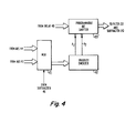
- FIGURE 4 shows an alternative embodiment of a portion of the attenuation network.
- four bit samples from multiplexer 45 are applied to a priority encoder 47 which provides a two bit output signal.
- the signal provided by the priority encoder indicates the position of the most significant one in the four bits from multiplexer 45.
- Priority encoder 47 is a simple digital circuit which may be built from standard logic elements by one skilled in the art.
- the two bit digital signal from priority encoder 47 is applied to the control input of an attenuator 49' which in this embodiment is a programmable bit shifter.
- the data input port of shifter 49' is coupled to receive the chrominance samples from delay element 48 and the output port of shifter 49' is coupled to provide scaled chrominance samples to low pass filter 22 and subtracter 20.
- Programmable bit shifter 49' may, for example, be similar to the one described in U.S. Patent No. 4,383,304 entitled "Programmable Bit Shift Circuit”. Shifter 49' attenuates the samples provided to its data input port by a factor of 1, 1/2, 1/4, or 1/8 by shifting these samples to the right by 0, 1, 2 or 3 bit positions respectively. The number of bit positions to be shifted is determined by the signal applied to the control input port of programmable bit shifter 49.
- shifter 49 is responsive to the logical complement of the signals generated by priority encoder 47.
- the following table illustrates the correspondence between chrominance amplitude, the priority encoder output signals P1 and P2, and the attenuation factor applied by shifter 49'.
- the embodiments described above show open loop implementations of the present invention, since the attenuation factor is not developed from the filtered signal. Closed loop implementations are also contemplated.
- the four most significant bits of the chrominance amplitude signal developed by the automatic chrominance control circuitry (not shown) or the chrominance overload detection circuitry (not shown) of the television receiver may be used as an attenuation factor. This factor may be applied to sample scaler 49 or to the combination of priority encoder 47 and programmable shifter 49'.
- Samples that have been conditioned by the frequency characteristic of the adaptive filtering system are available at the output port of adder 26. These sampled are applied to one of the two input ports of adder 30 and to the subtrahend input port of subtracter 32.
- Luminance samples from output port Y of comb filter 12 are coupled to the second input port adder 30 via delay element 28. Delay element 28 compensates for the processing time through the filtering system described above.
- Adder 30 restores the vertical detail information extracted from the combed chrominance signals to the combed luminance signals, to provide output luminance signals Y'.
- Combed chrominance samples from the C output port of comb filter 12 are coupled to the minuend input port of subtracter 32 via delay element 31.
- Delay element 31 provides sufficient delay so that the samples applied to the minuend input port of subtracter 32 correspond to the filtered samples applied to its subtrahend input port.
- Subtracter 32 removes vertical detail information from the combed chrominance signal and provides output chrominance signals C'.
- the vertical detail information provided by adder 26 has a relatively wide bandwidth.
- this vertical detail signal is added to the luminance signal in adder 30, the vertical resolution of the resultant luminance signal is relatively large.
- the wide bandwidth vertical detail signal is subtracted from the chrominance signal in subtracter 32, the bandwidth of the resultant chrominance signal is relatively narrow.
- the present embodiment uses two low pass filters to obtain an adaptive low pass response, it is contemplated that the invention may be practiced using any combination of low pass, band pass or high pass filters. Moreover, the invention is not limited to using the amplitude of a component of the input signal to control the shape of the frequency characteristic of adaptive filter system. It is contemplated that the frequency composition of a component or the relative amplitude or frequency composition of two or more components may also be used to control the shape of the characteristic.
Landscapes
- Engineering & Computer Science (AREA)
- Multimedia (AREA)
- Signal Processing (AREA)
- Processing Of Color Television Signals (AREA)
- Filters That Use Time-Delay Elements (AREA)
- Communication Control (AREA)
- Networks Using Active Elements (AREA)
- Separation By Low-Temperature Treatments (AREA)
- Electrotherapy Devices (AREA)
- Control Of El Displays (AREA)
Claims (10)
dadurch gekennzeichnet, daß
Priority Applications (1)
| Application Number | Priority Date | Filing Date | Title |
|---|---|---|---|
| AT85306872T ATE72502T1 (de) | 1984-10-04 | 1985-09-27 | Adaptives filtersystem. |
Applications Claiming Priority (2)
| Application Number | Priority Date | Filing Date | Title |
|---|---|---|---|
| US06/657,592 US4626894A (en) | 1984-10-04 | 1984-10-04 | Signal filtering system having adaptively cascaded filter stages for developing a variable bandwidth frequency characteristic |
| US657592 | 1984-10-04 |
Publications (3)
| Publication Number | Publication Date |
|---|---|
| EP0177285A2 EP0177285A2 (de) | 1986-04-09 |
| EP0177285A3 EP0177285A3 (en) | 1988-03-23 |
| EP0177285B1 true EP0177285B1 (de) | 1992-02-05 |
Family
ID=24637853
Family Applications (1)
| Application Number | Title | Priority Date | Filing Date |
|---|---|---|---|
| EP85306872A Expired - Lifetime EP0177285B1 (de) | 1984-10-04 | 1985-09-27 | Adaptives Filtersystem |
Country Status (11)
| Country | Link |
|---|---|
| US (1) | US4626894A (de) |
| EP (1) | EP0177285B1 (de) |
| JP (1) | JPH07105962B2 (de) |
| KR (1) | KR940011030B1 (de) |
| CN (1) | CN1004393B (de) |
| AT (1) | ATE72502T1 (de) |
| AU (1) | AU573037B2 (de) |
| CA (1) | CA1228669A (de) |
| DD (1) | DD238144A5 (de) |
| DE (1) | DE3585354D1 (de) |
| ES (1) | ES8705179A1 (de) |
Cited By (1)
| Publication number | Priority date | Publication date | Assignee | Title |
|---|---|---|---|---|
| US7881692B2 (en) | 2004-06-30 | 2011-02-01 | Silicon Laboratories Inc. | Integrated low-IF terrestrial audio broadcast receiver and associated method |
Families Citing this family (14)
| Publication number | Priority date | Publication date | Assignee | Title |
|---|---|---|---|---|
| US4686561A (en) * | 1985-07-31 | 1987-08-11 | Rca Corporation | Vertical detail information restoration circuit |
| US4827528A (en) * | 1985-11-15 | 1989-05-02 | Stanford University | Error-minimizing noise-reduction system |
| US4916526A (en) * | 1986-01-31 | 1990-04-10 | Yves C. Faroudja | Bandwidth control for chrominance and luminance paths in quadrature modulated color television system |
| JPS62245894A (ja) * | 1986-04-18 | 1987-10-27 | Sony Corp | 映像信号分離装置 |
| US4703340A (en) * | 1986-05-02 | 1987-10-27 | Rca Corporation | Frequency division multiplexed analog to digital converter |
| US4847682A (en) * | 1987-12-18 | 1989-07-11 | North American Philips Corporation | Adaptive comb filter for artifact-free decoding |
| JP2558922B2 (ja) * | 1990-05-15 | 1996-11-27 | 三菱電機株式会社 | Y/c分離装置 |
| KR930008184B1 (ko) * | 1990-06-30 | 1993-08-26 | 삼성전자 주식회사 | 휘도/색신호 분리 회로 |
| US6657597B2 (en) * | 2001-08-06 | 2003-12-02 | Halliburton Energy Services, Inc. | Directional signal and noise sensors for borehole electromagnetic telemetry system |
| US6781521B1 (en) * | 2001-08-06 | 2004-08-24 | Halliburton Energy Services, Inc. | Filters for canceling multiple noise sources in borehole electromagnetic telemetry system |
| US7218737B1 (en) * | 2002-08-21 | 2007-05-15 | Silicon Image, Inc. | System and method for an adaptive state machine to control signal filtering in a serial link |
| GB2426881B (en) * | 2005-06-01 | 2010-12-29 | Snell & Wilcox Ltd | Method and apparatus for spatial interpolation of colour images |
| CN103067014A (zh) * | 2012-12-25 | 2013-04-24 | 上海贝岭股份有限公司 | 用于谐波检测的频率跟随数据采集电路 |
| WO2015100522A1 (en) * | 2013-12-30 | 2015-07-09 | Mediatek Singapore Pte. Ltd. | Methods for inter-component residual prediction |
Family Cites Families (22)
| Publication number | Priority date | Publication date | Assignee | Title |
|---|---|---|---|---|
| US3242259A (en) * | 1961-03-31 | 1966-03-22 | Philco Corp | System to minimize desaturation and reduce noise in color tv picture by subtracting from luminance signal a d. c. signal derived from chrominance signal via a forward biased unilaterally conductive device |
| US4143397A (en) * | 1976-04-19 | 1979-03-06 | Rca Corporation | Comb filter apparatus |
| US4097897A (en) * | 1977-04-22 | 1978-06-27 | General Electric Company | Automatic boost control in an aperture corrector for TV video signals |
| US4149181A (en) * | 1977-09-02 | 1979-04-10 | Gte Sylvania Incorporated | Signal-dependent chrominance subcarrier filtering circuit |
| US4167021A (en) * | 1977-12-12 | 1979-09-04 | Rca Corporation | Suppression of chrominance signal contamination of the luminance signal in a video signal processing system |
| DE2810697C2 (de) * | 1978-03-11 | 1987-01-08 | Robert Bosch Gmbh, 7000 Stuttgart | Verfahren zur Trennung des Farbartsignals vom Leuchtdichtesignal bei Farbfernsehsignalen mit quadraturmodulierten Farbhilfsträgern |
| NL7803910A (nl) * | 1978-04-13 | 1979-10-16 | Philips Nv | Kamfilterschakeling. |
| JPS54139333A (en) * | 1978-04-20 | 1979-10-29 | Hitachi Ltd | Color television receiver |
| JPS54149515A (en) * | 1978-05-17 | 1979-11-22 | Nec Corp | Separator circuit for luminance signal and chromaticity signal |
| JPS5510228A (en) * | 1978-07-05 | 1980-01-24 | Nec Corp | S/n improving unit for television video signal |
| GB2034138B (en) * | 1978-09-26 | 1983-03-23 | Pioneer Electronic Corp | Variable gain amplifier circuit |
| IT1118625B (it) * | 1979-05-11 | 1986-03-03 | Cselt Centro Studi Lab Telecom | Perfezionamenti agli equializzatori per trasmissione di segnali numeri ci |
| US4245238A (en) * | 1979-05-11 | 1981-01-13 | Rca Corporation | Non-linear processing of video image vertical detail information |
| JPS5652441A (en) * | 1979-10-05 | 1981-05-11 | Pioneer Electronic Corp | Programmable bit shift circuit |
| JPS5760791A (en) * | 1980-09-30 | 1982-04-12 | Toshiba Corp | Demodulating circuit for wide-band receiving chrominance |
| US4415918A (en) * | 1981-08-31 | 1983-11-15 | Rca Corporation | Digital color television signal demodulator |
| GB2110044A (en) * | 1981-11-06 | 1983-06-08 | Rca Corp | Digital signal separation network and television receiver including such a network |
| US4524423A (en) * | 1981-11-06 | 1985-06-18 | Rca Corporation | Digital signal separation filters |
| US4443817A (en) * | 1981-11-25 | 1984-04-17 | Faroudja Y C | Chroma noise reduction system for quadrature modulated color television picture signals |
| JPS58123292A (ja) * | 1982-01-19 | 1983-07-22 | Pioneer Electronic Corp | 色ノイズ抑制回路 |
| GB2127250B (en) * | 1982-09-20 | 1986-04-09 | British Broadcasting Corp | Colour video signal processing |
| JPS58129892A (ja) * | 1983-01-28 | 1983-08-03 | Hitachi Ltd | 輝度・色信号分離回路 |
-
1984
- 1984-10-04 US US06/657,592 patent/US4626894A/en not_active Expired - Fee Related
-
1985
- 1985-09-16 CA CA000490855A patent/CA1228669A/en not_active Expired
- 1985-09-27 ES ES547387A patent/ES8705179A1/es not_active Expired
- 1985-09-27 EP EP85306872A patent/EP0177285B1/de not_active Expired - Lifetime
- 1985-09-27 AU AU47943/85A patent/AU573037B2/en not_active Ceased
- 1985-09-27 DE DE8585306872T patent/DE3585354D1/de not_active Expired - Fee Related
- 1985-09-27 AT AT85306872T patent/ATE72502T1/de not_active IP Right Cessation
- 1985-09-27 CN CN85107193.7A patent/CN1004393B/zh not_active Expired
- 1985-10-02 KR KR1019850007259A patent/KR940011030B1/ko not_active Expired - Fee Related
- 1985-10-02 DD DD85281349A patent/DD238144A5/de not_active IP Right Cessation
- 1985-10-03 JP JP60219323A patent/JPH07105962B2/ja not_active Expired - Lifetime
Cited By (4)
| Publication number | Priority date | Publication date | Assignee | Title |
|---|---|---|---|---|
| US7881692B2 (en) | 2004-06-30 | 2011-02-01 | Silicon Laboratories Inc. | Integrated low-IF terrestrial audio broadcast receiver and associated method |
| US8060049B2 (en) | 2004-06-30 | 2011-11-15 | Silicon Laboratories Inc. | Integrated low-if terrestrial audio broadcast receiver and associated method |
| US8249543B2 (en) | 2004-06-30 | 2012-08-21 | Silicon Laboratories Inc. | Low-IF integrated data receiver and associated methods |
| US8532601B2 (en) | 2004-06-30 | 2013-09-10 | Silicon Laboratories Inc. | Integrated low-IF terrestrial audio broadcast receiver and associated method |
Also Published As
| Publication number | Publication date |
|---|---|
| JPS6190594A (ja) | 1986-05-08 |
| KR940011030B1 (ko) | 1994-11-22 |
| DE3585354D1 (de) | 1992-03-19 |
| KR860003705A (ko) | 1986-05-28 |
| ATE72502T1 (de) | 1992-02-15 |
| EP0177285A2 (de) | 1986-04-09 |
| CN1004393B (zh) | 1989-05-31 |
| CA1228669A (en) | 1987-10-27 |
| ES8705179A1 (es) | 1987-04-16 |
| ES547387A0 (es) | 1987-04-16 |
| CN85107193A (zh) | 1986-07-16 |
| EP0177285A3 (en) | 1988-03-23 |
| AU573037B2 (en) | 1988-05-26 |
| JPH07105962B2 (ja) | 1995-11-13 |
| DD238144A5 (de) | 1986-08-06 |
| AU4794385A (en) | 1986-04-10 |
| US4626894A (en) | 1986-12-02 |
Similar Documents
| Publication | Publication Date | Title |
|---|---|---|
| US4626894A (en) | Signal filtering system having adaptively cascaded filter stages for developing a variable bandwidth frequency characteristic | |
| KR910004310B1 (ko) | 디지털 필터 | |
| CA1233240A (en) | Video signal recursive filter with luma/chroma separation | |
| MXPA97008123A (en) | Luma / chrome separation filter with derressive element co | |
| KR19990007950A (ko) | 공통 지연 소자를 갖는 휘도/색차 분리필터 | |
| US4651196A (en) | Adaptive control of the chrominance signal frequency response in a video signal processing system | |
| EP0169035B1 (de) | Schaltung zur Verarbeitung von Farbdifferenzsignalen | |
| EP0549174B1 (de) | Steuerung für adaptive Chromafilterung | |
| EP0153757A2 (de) | Digitale Fernsehsignal-Verarbeitungsschaltung | |
| EP0065881B1 (de) | System zur Filterung von Fernsehsignalen | |
| US6437827B1 (en) | Filtering video signals containing chrominance information | |
| KR930006457B1 (ko) | 디지탈 비디오 신호 처리 장치 | |
| US5150203A (en) | Variable chrominance filtering for encoding television signals | |
| JPH07118813B2 (ja) | カラー映像信号エンコード方法 | |
| EP0107463B1 (de) | Digitales Fernsehsystem mit Fehlerkorrektur | |
| EP0433866B1 (de) | Verfahren und Apparat zur Verminderung von Rauschimpulsen in digitalen Fernsehempfängern | |
| EP0122096B1 (de) | Chrominanz-invertierendes Allpassfilter | |
| KR940005177B1 (ko) | 펄스패턴 억압회로를 사용하는 필터회로를 갖는 휘도/색신호 분리회로 | |
| KR950004652Y1 (ko) | 휘도 및 색신호분리장치 | |
| JPS62145992A (ja) | くし形フイルタ回路 | |
| JPH01236890A (ja) | Y/c分離回路 | |
| JPS59122289A (ja) | コントラスト回路 | |
| JPH08336154A (ja) | ディジタルカラーエンコーダ | |
| JPH09233493A (ja) | 映像信号処理回路 | |
| JPH01284192A (ja) | 色信号処理回路 |
Legal Events
| Date | Code | Title | Description |
|---|---|---|---|
| PUAI | Public reference made under article 153(3) epc to a published international application that has entered the european phase |
Free format text: ORIGINAL CODE: 0009012 |
|
| AK | Designated contracting states |
Kind code of ref document: A2 Designated state(s): AT DE FR GB IT |
|
| PUAL | Search report despatched |
Free format text: ORIGINAL CODE: 0009013 |
|
| AK | Designated contracting states |
Kind code of ref document: A3 Designated state(s): AT DE FR GB IT |
|
| RAP1 | Party data changed (applicant data changed or rights of an application transferred) |
Owner name: RCA LICENSING CORPORATION |
|
| 17P | Request for examination filed |
Effective date: 19880826 |
|
| 17Q | First examination report despatched |
Effective date: 19900629 |
|
| GRAA | (expected) grant |
Free format text: ORIGINAL CODE: 0009210 |
|
| AK | Designated contracting states |
Kind code of ref document: B1 Designated state(s): AT DE FR GB IT |
|
| REF | Corresponds to: |
Ref document number: 72502 Country of ref document: AT Date of ref document: 19920215 Kind code of ref document: T |
|
| ITF | It: translation for a ep patent filed | ||
| REF | Corresponds to: |
Ref document number: 3585354 Country of ref document: DE Date of ref document: 19920319 |
|
| ET | Fr: translation filed | ||
| PG25 | Lapsed in a contracting state [announced via postgrant information from national office to epo] |
Ref country code: AT Effective date: 19920927 |
|
| PLBE | No opposition filed within time limit |
Free format text: ORIGINAL CODE: 0009261 |
|
| STAA | Information on the status of an ep patent application or granted ep patent |
Free format text: STATUS: NO OPPOSITION FILED WITHIN TIME LIMIT |
|
| 26N | No opposition filed | ||
| PGFP | Annual fee paid to national office [announced via postgrant information from national office to epo] |
Ref country code: DE Payment date: 19980724 Year of fee payment: 14 |
|
| PGFP | Annual fee paid to national office [announced via postgrant information from national office to epo] |
Ref country code: GB Payment date: 19980727 Year of fee payment: 14 |
|
| PGFP | Annual fee paid to national office [announced via postgrant information from national office to epo] |
Ref country code: FR Payment date: 19980803 Year of fee payment: 14 |
|
| PG25 | Lapsed in a contracting state [announced via postgrant information from national office to epo] |
Ref country code: GB Free format text: LAPSE BECAUSE OF NON-PAYMENT OF DUE FEES Effective date: 19990927 |
|
| GBPC | Gb: european patent ceased through non-payment of renewal fee |
Effective date: 19990927 |
|
| PG25 | Lapsed in a contracting state [announced via postgrant information from national office to epo] |
Ref country code: FR Free format text: LAPSE BECAUSE OF NON-PAYMENT OF DUE FEES Effective date: 20000531 |
|
| PG25 | Lapsed in a contracting state [announced via postgrant information from national office to epo] |
Ref country code: DE Free format text: LAPSE BECAUSE OF NON-PAYMENT OF DUE FEES Effective date: 20000701 |
|
| REG | Reference to a national code |
Ref country code: FR Ref legal event code: ST |