EP0178619A2 - Verfahren zur Bildung eines Leitermusters - Google Patents
Verfahren zur Bildung eines Leitermusters Download PDFInfo
- Publication number
- EP0178619A2 EP0178619A2 EP85113017A EP85113017A EP0178619A2 EP 0178619 A2 EP0178619 A2 EP 0178619A2 EP 85113017 A EP85113017 A EP 85113017A EP 85113017 A EP85113017 A EP 85113017A EP 0178619 A2 EP0178619 A2 EP 0178619A2
- Authority
- EP
- European Patent Office
- Prior art keywords
- conductive layer
- pattern
- masking
- forming
- mask
- Prior art date
- Legal status (The legal status is an assumption and is not a legal conclusion. Google has not performed a legal analysis and makes no representation as to the accuracy of the status listed.)
- Granted
Links
Images



Classifications
-
- H—ELECTRICITY
- H10—SEMICONDUCTOR DEVICES; ELECTRIC SOLID-STATE DEVICES NOT OTHERWISE PROVIDED FOR
- H10D—INORGANIC ELECTRIC SEMICONDUCTOR DEVICES
- H10D30/00—Field-effect transistors [FET]
- H10D30/01—Manufacture or treatment
- H10D30/061—Manufacture or treatment of FETs having Schottky gates
- H10D30/0612—Manufacture or treatment of FETs having Schottky gates of lateral single-gate Schottky FETs
- H10D30/0616—Manufacture or treatment of FETs having Schottky gates of lateral single-gate Schottky FETs using processes wherein the final gate is made before the completion of the source and drain regions, e.g. gate-first processes
-
- H—ELECTRICITY
- H10—SEMICONDUCTOR DEVICES; ELECTRIC SOLID-STATE DEVICES NOT OTHERWISE PROVIDED FOR
- H10P—GENERIC PROCESSES OR APPARATUS FOR THE MANUFACTURE OR TREATMENT OF DEVICES COVERED BY CLASS H10
- H10P50/00—Etching of wafers, substrates or parts of devices
- H10P50/20—Dry etching; Plasma etching; Reactive-ion etching
- H10P50/26—Dry etching; Plasma etching; Reactive-ion etching of conductive or resistive materials
- H10P50/264—Dry etching; Plasma etching; Reactive-ion etching of conductive or resistive materials by chemical means
- H10P50/266—Dry etching; Plasma etching; Reactive-ion etching of conductive or resistive materials by chemical means by vapour etching only
- H10P50/267—Dry etching; Plasma etching; Reactive-ion etching of conductive or resistive materials by chemical means by vapour etching only using plasmas
-
- H—ELECTRICITY
- H10—SEMICONDUCTOR DEVICES; ELECTRIC SOLID-STATE DEVICES NOT OTHERWISE PROVIDED FOR
- H10P—GENERIC PROCESSES OR APPARATUS FOR THE MANUFACTURE OR TREATMENT OF DEVICES COVERED BY CLASS H10
- H10P50/00—Etching of wafers, substrates or parts of devices
- H10P50/20—Dry etching; Plasma etching; Reactive-ion etching
- H10P50/26—Dry etching; Plasma etching; Reactive-ion etching of conductive or resistive materials
- H10P50/264—Dry etching; Plasma etching; Reactive-ion etching of conductive or resistive materials by chemical means
- H10P50/266—Dry etching; Plasma etching; Reactive-ion etching of conductive or resistive materials by chemical means by vapour etching only
- H10P50/267—Dry etching; Plasma etching; Reactive-ion etching of conductive or resistive materials by chemical means by vapour etching only using plasmas
- H10P50/268—Dry etching; Plasma etching; Reactive-ion etching of conductive or resistive materials by chemical means by vapour etching only using plasmas of silicon-containing layers
-
- H—ELECTRICITY
- H10—SEMICONDUCTOR DEVICES; ELECTRIC SOLID-STATE DEVICES NOT OTHERWISE PROVIDED FOR
- H10P—GENERIC PROCESSES OR APPARATUS FOR THE MANUFACTURE OR TREATMENT OF DEVICES COVERED BY CLASS H10
- H10P76/00—Manufacture or treatment of masks on semiconductor bodies, e.g. by lithography or photolithography
- H10P76/20—Manufacture or treatment of masks on semiconductor bodies, e.g. by lithography or photolithography of masks comprising organic materials
- H10P76/202—Manufacture or treatment of masks on semiconductor bodies, e.g. by lithography or photolithography of masks comprising organic materials for lift-off processes
Definitions
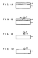
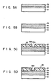
- a metal layer 2 is formed on a semiconductor substrate 1.
- a photoresist pattern 3 is formed on target region 2a of the metal layer 2 to carry an electrode pattern thereon.
- the metal layer 2 is subjected to reactive ion etching using the photoresist pattern 3 as a mask, thus forming a metal electrode pattern 2a.
- the photoresist pattern 3 is removed to leave the metal electrode pattern 2a alone on the semiconductor substrate 1.
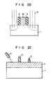
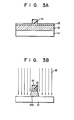
- the titanium layer 13 and the gold layer 12 are selectively removed by the ion milling method using the photoresist pattern 14 as a mask. In doing this, accelerated argon particles 15 are impinged on the surface of the structure to selectively remove the titanium layer 13 first and then the gold layer 12. In removing the gold layer 12, the photoresist pattern 14 and the remaining titanium layer 13 are used as a mask. Thus, a gold electrode pattern 12a is formed.
- the selective removal of the conductor layer by anisotropic etching can be accomplished by the use of the first masking metal pattern as a mask.
- this purpose may be achieved by using a second masking metal pattern as a mask which is formed using the first masking metal pattern as a mask.
- the material forming the first masking metal film needs to have etching selectivity for the material of the conductive layer.
- gold, titanium, aluminum, tungsten, molybdenum, etc. may be used for the first masking metal film.
- the conductive layer 22 forms a Schottky junction at the surface in contact with the substrate 21.
- a photoresist film 23 is formed on the whole surface of the conductive layer 22 but a portion 22a thereof which is to constitute a gate electrode pattern.
- an insulating layer or a side wall 25 is formed as required on the lateral face of the electrode pattern 22a.
- an n-type impurity is injected at a high concentration into the semiconductor substrate 21 by ion implantation, thus forming an n + region (source 27a and drain 27b).
- Example 1 titanium, which is hardly affected by reactive ion etching when CF 4 + 0 2 gas is used as etching gas, is used for the etching mask. Therefore, the etching mask can be made thinner, and the dimensional change between the etching mask and the metal electrode pattern is reduced. Conventionally, a photoresist is used for the etching mask. It is very difficult, however, to form a thick and narrow photoresist film, so that a fine electrode pattern is difficult to form. According to Example 1, the photoresist film is stable enough to facilitate the formation of a fine electrode pattern, since it is formed over a wide region except the electrode pattern portion.
- the etching mask is a metal (titanium) film which is highly resistant to reactive ion etching when CF 4 + 0 2 gas is used as etching gas. Even if reduced to e.g. 0.5 microns or less in thickness, therefore, the etching mask will never peel off during the etching process.
- the metal or titanium film as the etching mask is barely susceptible to side etching by the reactive ion etching method using CF 4 + 0 2 gas. Therefore, the electrode pattern does not become trapezoidal or semicircular in vertical sectional shape due to side etching. Thus, the resistivity of the electrode pattern is not increased and the high-frequency characteristics are not degraded.
- the present invention is not limited to the embodiment described above, and the same effect may be obtained with use of reactive ion etching as the reactive ion etching method using chlorine-based gas in which the conductive layer is formed of aluminum and the masking metal film is a gold film with a thickness of 500 to 1,000 angstroms. Moreover, any number of other metal materials with high etching selectivity for reactive ion etching may be used individually for the conductive layer and the masking metal film with the same result.
- the conductive layer is not limited to metal, and may alternatively be formed of, for example, polycrystalline silicon.
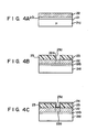
- a metal layer e.g., a tungsten nitride layer 35
- a gold layer 32 is formed to a thickness of 0.5 micron on the tungsten nitride layer 35.
- the tungsten nitride layer 35 and the gold layer 32 are metal layers which finally form a gate electrode G.
- the gold layer 32 serves to lower the resistivity of the gate electrode.
- a second masking conductive layer e.g., a tungsten layer 36, is deposited to a thickness of 0.1 pm on the whole surface of the gold layer 32.
- a first masking conductive layer e.g., a titanium layer 38
- a first masking conductive layer is deposited to a thickness of 0.1 ⁇ m on the photoresist film 37 and the mask portion 36a of the tungsten layer 36 exposed through the opening 37a.
- the titanium layer 38 is thinned at the portion on the side wall of the opening 37a.
- the gold layer 32 and the tungsten nitride layer 35 thereunder are selectively removed by anisotropic dry etching, e.g., ion milling using argon ions, with the aid of the titanium layer portion 38a and the mask portion 36a of the tungsten layer 36 as a mask.
- anisotropic dry etching e.g., ion milling using argon ions
- Example 2 a fine opening pattern of the same shape as the gate electrode pattern to be obtained is formed in the photoresist film, so that the photoresist film is put on the underlying metal layer (tungsten layer) with a wide contact area. Therefore, the mask pattern can reliably and easily made finer, permitting formation of a finer gate electrode pattern and hence a gate electrode with a short gate length. If the gate length is shortened, the contact area between the gate electrode and the semiconductor substrate (dhannel region) will be reduced in proportion. As a result, the input capacitance and feedback capacitance are reduced. Thus, it is possible to produce an MESFET with improved high-frequency characteristics, e.g., lower noise, higher transconductance, greater gain, etc.
- Example 2 the second masking conductive layer (tungsten layer) is patterned by reactive ion etching with the aid of the first masking conductive layer (titanium layer) as a mask.
- the reactive ion etching permits substantial reduction of the dimensional change between the mask and the pattern of the etched material formed with the aid of the mask. It is therefore possible to pattern the second masking conductive layer according to the dimensions specified for the first masking conductive layer.
- the titanium layer as the first masking conductive layer which is resistant to reactive ion etching in which CF 4 + 0 2 gas is used, is about 0.1 pm thick.
- This thickness is as small as about one-tenth that of the photoresist film used in the prior art example. Accordingly, the dimensional change is smaller when the titanium layer is used as a mask than in the conventional case where the photoresist film is used as the mask. Namely, in Example 2, the difference between the pattern widths of the mask and the electrode formed therewith is reduced.
- the electrode patterning can be performed more accurately based on the dimensions determined of the mask than in the prior art case. Since the dimensional change is small, moreover, the vertical section of the formed gate electrode is substantially rectangular in shape, having its topside length substantially equal to the base length (gate length): If the base length (gate length) is taken as a basis, the vertical section of the rectangular gate electrode is greater than that of the conventional trapezoidal electrode whose topside is shorter than its base. Therefore, the gate electrode is formed by the method of Example 2 is lowered in resistivity.
- Example 2 the titanium layer is resistant to ion milling using argon particles, so that the etching time can be made longer than in the prior art method which uses photoresist for the mask. Thus, it is possible to pattern even a relatively thick electrode.
- the mask pattern of the tungsten layer as the second masking conductive layer is formed with use of the titanium layer as the first masking conductive layer as a mask, by reactive ion etching using CF 4 + 0 2 gas.
- the reactive ion etching method the chemical reactivity of the gas mixture is utilized for good control in side etching of the lateral face portions of the mask. Accordingly, the mask pattern of the tungsten layer as the second masking conductive layer, which is finer than the titanium layer mask as the first masking conductive layer, can be formed with good control.
- the gate electrode can be made finer than the titanium film mask as the first masking conductive layer.
- the first and second masking conductive layers may be formed from aluminum and molybdenum, respectively.
- the first and second conductive layers may be formed from gold and titanium, respectively, so that the titanium layer may be subjected to reactive ion etching using chlorine-based gas with the aid of the gold layer as a mask.
Landscapes
- Junction Field-Effect Transistors (AREA)
- Drying Of Semiconductors (AREA)
Applications Claiming Priority (4)
| Application Number | Priority Date | Filing Date | Title |
|---|---|---|---|
| JP59216316A JPS6196765A (ja) | 1984-10-17 | 1984-10-17 | 金属パタ−ン形成方法 |
| JP59216317A JPS6196735A (ja) | 1984-10-17 | 1984-10-17 | 導体パタ−ン形成方法 |
| JP216317/84 | 1984-10-17 | ||
| JP216316/84 | 1984-10-17 |
Publications (3)
| Publication Number | Publication Date |
|---|---|
| EP0178619A2 true EP0178619A2 (de) | 1986-04-23 |
| EP0178619A3 EP0178619A3 (en) | 1988-09-14 |
| EP0178619B1 EP0178619B1 (de) | 1990-07-18 |
Family
ID=26521361
Family Applications (1)
| Application Number | Title | Priority Date | Filing Date |
|---|---|---|---|
| EP85113017A Expired EP0178619B1 (de) | 1984-10-17 | 1985-10-14 | Verfahren zur Bildung eines Leitermusters |
Country Status (3)
| Country | Link |
|---|---|
| US (1) | US4674174A (de) |
| EP (1) | EP0178619B1 (de) |
| DE (1) | DE3578729D1 (de) |
Cited By (7)
| Publication number | Priority date | Publication date | Assignee | Title |
|---|---|---|---|---|
| EP0276902A1 (de) * | 1987-01-12 | 1988-08-03 | Itt Industries, Inc. | Verfahren zum Herstellen eines Feldeffekttransistors |
| EP0275905A3 (de) * | 1987-01-20 | 1989-08-30 | International Standard Electric Corporation | Selbstausgerichteter Feldeffekttransistor und Verfahren zur Herstellung |
| EP0553006A3 (de) * | 1992-01-24 | 1993-08-11 | Thomson-Csf Semiconducteurs Specifiques | Verfahren zur Herstellung eines Transistors |
| EP0540230A3 (en) * | 1991-10-28 | 1993-08-25 | American Telephone And Telegraph Company | Method for forming patterned tungsten layers |
| EP0501428A3 (en) * | 1991-02-25 | 1995-01-18 | Sumitomo Electric Industries | Production methods for a compound semiconductor device |
| EP0630044A3 (de) * | 1988-09-08 | 1995-03-29 | Tokyo Shibaura Electric Co | Herstellung von einem vorbeschriebenem Muster über eine Halbleitervorrichtungsschicht. |
| WO2010010176A1 (fr) * | 2008-07-25 | 2010-01-28 | Commissariat A L'energie Atomique | Procede de microstructuration d'une couche de diamant |
Families Citing this family (16)
| Publication number | Priority date | Publication date | Assignee | Title |
|---|---|---|---|---|
| US4811078A (en) * | 1985-05-01 | 1989-03-07 | Texas Instruments Incorporated | Integrated circuit device and process with tin capacitors |
| US4821085A (en) * | 1985-05-01 | 1989-04-11 | Texas Instruments Incorporated | VLSI local interconnect structure |
| US4814854A (en) * | 1985-05-01 | 1989-03-21 | Texas Instruments Incorporated | Integrated circuit device and process with tin-gate transistor |
| US5027166A (en) * | 1987-12-04 | 1991-06-25 | Sanken Electric Co., Ltd. | High voltage, high speed Schottky semiconductor device and method of fabrication |
| US5025303A (en) * | 1988-02-26 | 1991-06-18 | Texas Instruments Incorporated | Product of pillar alignment and formation process |
| US4923827A (en) * | 1988-05-16 | 1990-05-08 | Eaton Corporation | T-type undercut electrical contact process on a semiconductor substrate |
| US4935805A (en) * | 1988-05-16 | 1990-06-19 | Eaton Corporation | T-type undercut electrical contact on a semiconductor substrate |
| US5153754A (en) * | 1989-06-30 | 1992-10-06 | General Electric Company | Multi-layer address lines for amorphous silicon liquid crystal display devices |
| GB2237929A (en) * | 1989-10-23 | 1991-05-15 | Philips Electronic Associated | A method of manufacturing a semiconductor device |
| DE69128123T2 (de) * | 1990-08-31 | 1998-03-05 | Texas Instruments Inc | Verfahren zum Herstellen selbst-ausrichtender bipolarer Transistoren mit Heteroübergang |
| US5536666A (en) * | 1994-06-03 | 1996-07-16 | Itt Corporation | Method for fabricating a planar ion-implanted GaAs MESFET with improved open-channel burnout characteristics |
| KR19980060606A (ko) * | 1996-12-31 | 1998-10-07 | 김영환 | 반도체 소자의 금속배선 형성 방법 |
| US6420099B1 (en) * | 1999-08-02 | 2002-07-16 | Infineon Technologies Ag | Tungsten hard mask for dry etching aluminum-containing layers |
| JP2004071015A (ja) * | 2002-08-05 | 2004-03-04 | Fujitsu Ltd | 薄膜磁気ヘッドの製造方法 |
| NL1026013C2 (nl) | 2004-04-23 | 2005-10-25 | Otb Group Bv | Werkwijze en inrichting voor het nauwkeurig aanbrengen van structuren op een substraat. |
| US9917027B2 (en) * | 2015-12-30 | 2018-03-13 | Globalfoundries Singapore Pte. Ltd. | Integrated circuits with aluminum via structures and methods for fabricating the same |
Family Cites Families (6)
| Publication number | Priority date | Publication date | Assignee | Title |
|---|---|---|---|---|
| DE1954499A1 (de) * | 1969-10-29 | 1971-05-06 | Siemens Ag | Verfahren zur Herstellung von Halbleiterschaltkreisen mit Leitbahnen |
| US4132586A (en) * | 1977-12-20 | 1979-01-02 | International Business Machines Corporation | Selective dry etching of substrates |
| US4362597A (en) * | 1981-01-19 | 1982-12-07 | Bell Telephone Laboratories, Incorporated | Method of fabricating high-conductivity silicide-on-polysilicon structures for MOS devices |
| CA1200624A (en) * | 1981-08-10 | 1986-02-11 | Susumu Muramoto | Method for the manufacture of semiconductor device using refractory metal in a lift-off step |
| US4400257A (en) * | 1982-12-21 | 1983-08-23 | Rca Corporation | Method of forming metal lines |
| US4586063A (en) * | 1984-04-02 | 1986-04-29 | Oki Electric Industry Co., Ltd. | Schottky barrier gate FET including tungsten-aluminum alloy |
-
1985
- 1985-10-11 US US06/786,825 patent/US4674174A/en not_active Expired - Lifetime
- 1985-10-14 EP EP85113017A patent/EP0178619B1/de not_active Expired
- 1985-10-14 DE DE8585113017T patent/DE3578729D1/de not_active Expired - Lifetime
Cited By (7)
| Publication number | Priority date | Publication date | Assignee | Title |
|---|---|---|---|---|
| EP0276902A1 (de) * | 1987-01-12 | 1988-08-03 | Itt Industries, Inc. | Verfahren zum Herstellen eines Feldeffekttransistors |
| EP0275905A3 (de) * | 1987-01-20 | 1989-08-30 | International Standard Electric Corporation | Selbstausgerichteter Feldeffekttransistor und Verfahren zur Herstellung |
| EP0630044A3 (de) * | 1988-09-08 | 1995-03-29 | Tokyo Shibaura Electric Co | Herstellung von einem vorbeschriebenem Muster über eine Halbleitervorrichtungsschicht. |
| EP0501428A3 (en) * | 1991-02-25 | 1995-01-18 | Sumitomo Electric Industries | Production methods for a compound semiconductor device |
| EP0540230A3 (en) * | 1991-10-28 | 1993-08-25 | American Telephone And Telegraph Company | Method for forming patterned tungsten layers |
| EP0553006A3 (de) * | 1992-01-24 | 1993-08-11 | Thomson-Csf Semiconducteurs Specifiques | Verfahren zur Herstellung eines Transistors |
| WO2010010176A1 (fr) * | 2008-07-25 | 2010-01-28 | Commissariat A L'energie Atomique | Procede de microstructuration d'une couche de diamant |
Also Published As
| Publication number | Publication date |
|---|---|
| US4674174A (en) | 1987-06-23 |
| EP0178619B1 (de) | 1990-07-18 |
| EP0178619A3 (en) | 1988-09-14 |
| DE3578729D1 (de) | 1990-08-23 |
Similar Documents
| Publication | Publication Date | Title |
|---|---|---|
| US4674174A (en) | Method for forming a conductor pattern using lift-off | |
| EP0448307B1 (de) | Verfahren zur Herstellung eines leitenden Elements | |
| US6033980A (en) | Method of forming submicron contacts and vias in an integrated circuit | |
| US4358340A (en) | Submicron patterning without using submicron lithographic technique | |
| US5220186A (en) | Semiconductor device with a mushroom-shaped gate electrode | |
| US4694564A (en) | Method for the manufacture of a Schottky gate field effect transistor | |
| JPS6196765A (ja) | 金属パタ−ン形成方法 | |
| US6111319A (en) | Method of forming submicron contacts and vias in an integrated circuit | |
| JPH0136250B2 (de) | ||
| US3951708A (en) | Method of manufacturing a semiconductor device | |
| EP0436192B1 (de) | Methode zur Herstellung eines Halbleiterbauelementes mit angeschrägten Öffnungen | |
| US4775644A (en) | Zero bird-beak oxide isolation scheme for integrated circuits | |
| US4400257A (en) | Method of forming metal lines | |
| EP0152164A2 (de) | Herstellung einer unter einem halben Mikrometer breiten Vertiefung in einem Halbleitersubstrat | |
| US5483089A (en) | Electrically isolated MESFET | |
| US4170500A (en) | Process for forming field dielectric regions in semiconductor structures without encroaching on device regions | |
| JPS60106142A (ja) | 半導体素子の製造方法 | |
| EP0120614A1 (de) | Verfahren zur Herstellung einer Halbleiteranordnung mit Isolationszonen | |
| US5237192A (en) | MESFET semiconductor device having a T-shaped gate electrode | |
| US6383853B2 (en) | Method of fabricating semiconductor device | |
| JPH09148449A (ja) | 半導体装置の製造方法 | |
| JPS6196735A (ja) | 導体パタ−ン形成方法 | |
| JP2709086B2 (ja) | 半導体装置の電極形成方法 | |
| US3923562A (en) | Process for producing monolithic circuits | |
| KR100272577B1 (ko) | 바이폴라 트랜지스터의 제조방법 |
Legal Events
| Date | Code | Title | Description |
|---|---|---|---|
| PUAI | Public reference made under article 153(3) epc to a published international application that has entered the european phase |
Free format text: ORIGINAL CODE: 0009012 |
|
| 17P | Request for examination filed |
Effective date: 19851111 |
|
| AK | Designated contracting states |
Kind code of ref document: A2 Designated state(s): DE FR GB |
|
| PUAL | Search report despatched |
Free format text: ORIGINAL CODE: 0009013 |
|
| AK | Designated contracting states |
Kind code of ref document: A3 Designated state(s): DE FR GB |
|
| 17Q | First examination report despatched |
Effective date: 19881215 |
|
| GRAA | (expected) grant |
Free format text: ORIGINAL CODE: 0009210 |
|
| AK | Designated contracting states |
Kind code of ref document: B1 Designated state(s): DE FR GB |
|
| REF | Corresponds to: |
Ref document number: 3578729 Country of ref document: DE Date of ref document: 19900823 |
|
| ET | Fr: translation filed | ||
| PLBE | No opposition filed within time limit |
Free format text: ORIGINAL CODE: 0009261 |
|
| STAA | Information on the status of an ep patent application or granted ep patent |
Free format text: STATUS: NO OPPOSITION FILED WITHIN TIME LIMIT |
|
| 26N | No opposition filed | ||
| PGFP | Annual fee paid to national office [announced via postgrant information from national office to epo] |
Ref country code: GB Payment date: 19971006 Year of fee payment: 13 |
|
| PGFP | Annual fee paid to national office [announced via postgrant information from national office to epo] |
Ref country code: DE Payment date: 19971017 Year of fee payment: 13 |
|
| PG25 | Lapsed in a contracting state [announced via postgrant information from national office to epo] |
Ref country code: GB Free format text: LAPSE BECAUSE OF NON-PAYMENT OF DUE FEES Effective date: 19981014 |
|
| GBPC | Gb: european patent ceased through non-payment of renewal fee |
Effective date: 19981014 |
|
| PG25 | Lapsed in a contracting state [announced via postgrant information from national office to epo] |
Ref country code: DE Free format text: LAPSE BECAUSE OF NON-PAYMENT OF DUE FEES Effective date: 19990803 |
|
| PGFP | Annual fee paid to national office [announced via postgrant information from national office to epo] |
Ref country code: FR Payment date: 20041008 Year of fee payment: 20 |