EP0178948A2 - Mémoire à accès aléatoire à transistors bipolaires ayant une configuration à redondance - Google Patents
Mémoire à accès aléatoire à transistors bipolaires ayant une configuration à redondance Download PDFInfo
- Publication number
- EP0178948A2 EP0178948A2 EP85307560A EP85307560A EP0178948A2 EP 0178948 A2 EP0178948 A2 EP 0178948A2 EP 85307560 A EP85307560 A EP 85307560A EP 85307560 A EP85307560 A EP 85307560A EP 0178948 A2 EP0178948 A2 EP 0178948A2
- Authority
- EP
- European Patent Office
- Prior art keywords
- power supply
- supply means
- node
- linked
- short
- Prior art date
- Legal status (The legal status is an assumption and is not a legal conclusion. Google has not performed a legal analysis and makes no representation as to the accuracy of the status listed.)
- Granted
Links
Images






Classifications
-
- G—PHYSICS
- G11—INFORMATION STORAGE
- G11C—STATIC STORES
- G11C29/00—Checking stores for correct operation ; Subsequent repair; Testing stores during standby or offline operation
- G11C29/70—Masking faults in memories by using spares or by reconfiguring
- G11C29/78—Masking faults in memories by using spares or by reconfiguring using programmable devices
- G11C29/84—Masking faults in memories by using spares or by reconfiguring using programmable devices with improved access time or stability
- G11C29/842—Masking faults in memories by using spares or by reconfiguring using programmable devices with improved access time or stability by introducing a delay in a signal path
-
- G—PHYSICS
- G11—INFORMATION STORAGE
- G11C—STATIC STORES
- G11C29/00—Checking stores for correct operation ; Subsequent repair; Testing stores during standby or offline operation
- G11C29/70—Masking faults in memories by using spares or by reconfiguring
- G11C29/78—Masking faults in memories by using spares or by reconfiguring using programmable devices
- G11C29/84—Masking faults in memories by using spares or by reconfiguring using programmable devices with improved access time or stability
- G11C29/846—Masking faults in memories by using spares or by reconfiguring using programmable devices with improved access time or stability by choosing redundant lines at an output stage
Definitions
- This invention relates to a bipolar-transistor type random access memory (RAM) having a redundancy configuration and, more particularly, to a defective address memory portion thereof.
- RAM bipolar-transistor type random access memory
- a large number of memory cells are arranged along rows and columns.
- the density of defects generated in such a semiconductor memory device during the manufacture thereof is relatively independent of the integration density of the device. Rather, it derives from the semiconductor manufacturing technology. In general, the higher the integration density of the device, the greater the ratio of normal memory cells to defective memory cells. This is one of the advantages of increasing the integration density of a semiconductor memory device.
- redundancy memory cells In a metal-insulator-semiconductor (MIS) RAM, in order to overcome the problem of defective memory cells, use is made of redundancy memory cells. When a defective memory cell is detected, a redundancy memory cell row or column is selected instead of the memory cell row or column including the defective memory cell. In general, one or two redundancy memory cell rows or columns are usually provided.
- MIS metal-insulator-semiconductor
- a defective address memory circuit in order to store address information of such a defective row or column and to disable regular decoders for selecting normal memory cells so as to select the redundancy row or column in response to an address of the defective row or column, a defective address memory circuit is required.
- a semiconductor memory device of a bipolar-transistor type comprising; a memory cell array; a redundancy memory cell array; means for receiving an address signal; means for selecting a normal memory cell from said memory cell array in accordance with said address signal from said address receiving means; means for storing a defective address of a defective memory cell of said memory cell array, said defective address storing means comprising a plurality of 1-bit memory circuits of a diode type, each circuit corresponding to each bit of said defective address; and means for comparing the address of said address signal from said address receiving means with said defective address of said defective address storing means so as to disable said normal memory cell selecting means and select said redundancy memory cell array when the address of said address signal is different from said defective address.
- an information memory circuit including at least three diode stages along a forward bias direction between a first power supply and a node; a diode stage linked along a backward bias direction between a write power supply and the first power supply; a shorted-junction type programmable read-only memory (PROM) cell linked between the write power supply V and the node; and a switching element linked between the node and a second power supply, thereby generating a high or low potential from the node in accordance with the short-circuited or non-short-circuited state of the PROM cell.
- PROM programmable read-only memory
- two diode stages can be provided instead of the three or more diode stages, and in this case, the diode along the backward bias direction is changed by one resistor, or one diode stage along a forward bias direction is provided on the side of the first power supply.
- an information memory circuit including at least three diode stages along a forward bias direction between a first power supply and a first node; a resistor linked between the first node and a second power supply; a diode stage linked between the first and second nodes and having the same conduction direction as the three or more diode stages; a resistor linked between the second node and the second power supply; a diode stage linked along a backward bias direction between the first power supply and a write power supply; a short-circuited-junction type PROM cell linked between the write power supply and the second node; and a switching element, linked between the second node and the second power supply; and an output circuit, connected to the first and second nodes, for detecting the difference in potential in accordance with the short-circuited or non-short-circuited state of the PROM cell.
- the diode between the first power supply and the write power supply can be replaced by a resistor, and one stage of the three diode stages can be omitted. Also, the diode stage between the first power supply and the write power supply can be detected. However, instead of this, a diode stage is provided on the first power supply.
- the short-circuited junction type PROM cell if the short-circuited junction type PROM cell is not destroyed, the potential at the first node is low. On the other hand, if the short-circuited junction type PROM cell is destroyed, the potential at the first node is high.
- the data of the PROM cell can be read out by detecting the potential at the first node. Note that the difference in potential at the first node between the non-destroyed state and the destroyed state of the PROM cell corresponds to the forward direction potential of one diode stage.
- a memory device comprises a 64K-bit static memory cell array 1, and a redundancy array 2.
- the redundancy array can comprise more than two rows or columns, but, in this case, a one-row array is described in order to simplify the explanation.
- One row of the memory cell array 1 is selected by row address butfers 3, word decoders 4, and word drivers 5.
- external row address signals A 0 , A 1 ..., A 7 are received by emitter-followers Q11 and are converted by the row address buffers 3 into internal row address signals A 0 , A 1 , ..., and A 7 , and their inverted signals A 0 , A 1 , ..., A 7 , which are received by the word decoders 4 which drive one of the 256 word drivers 5, i.e. one of the word lines WL O , WL 1 , ..., WL 255 .
- one column of the memory cell array 1 is selected by column selection means (not shown).
- the device further comprises a defective address memory circuit 6, an address comparing circuit 7 for comparing an input address defined by the external address signals A 0 , A 1 , ..., and A 7 with the defective address defined by signals A 0R , A 1R , ..., and A 7R stored in the defective address memory circuit 6, and a driver circuit 8 for driving the redundancy array 2.
- the circuit of Fig. 1 operates in the same way as the conventional devices. However, if a defective cell is detected in the memory cell array 1 of Fig. 1, the row address of a row including this defective cell (hereinafter referred to as a defective row address) is written into the defective address memory circuit 6.
- the row address signals A 0 , A 1 , ..., and A 7 are always compared with the defective address signals A 0R , A 1R , ..., and A 7R written into the address memory circuit 6.
- the address comparing circuit 7 operates the driver 8 to select the word line WL R and drive the redundancy array 2, and simultaneously to disable the word drivers 5, thereby causing non-selection of the memory cell array 1.
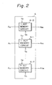
- the circuit 6 comprises 1-bit memory circuits 6-0, 6-1, ..., and 6-7 corresponding to each of the row address signals A 0 , A 1 , ..., and A 7 . That is, the row address signals A 0 , A 1 , ..., and A 7 are applied thereto, a high voltage such as +5 V is applied as a write voltage to the write terminal V P , and a low voltage such as -5 V is applied to the other terminal V n . Then, the row address signals A 0 , A 1 , ..., and A 7 are written into the 1-bit memory circuits 6-0, 6-1, ..., and 6-7, respectively. Thus, these signals can be read out as the defective address signals, ..., A 0R , A 1R , ..., and A 7R .
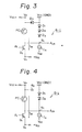
- Fig. 3 which illustrates a first example of the 1-bit memory circuit of Fig. 2
- power supply V CC is, for example, the ground level GND
- power supply V EE is, for example, -5 V.
- the write power supply Vp is +5 V, otherwise Vp equals V CC (GND).
- the write power supply V n is lower than -5 V, otherwise V n equals V EE (-5 V).
- PC designates a short-circuited junction type PROM cell which has diode characteristics after a write mode. That is, during a write mode, a larger voltage than the endurance voltage C E of the PROM cell, which is a kind of transistor, is applied to the emitter-collector thereof, thereby breaking it down.
- diode stage D 1 is provided between the power supply V CC and node N 1 between the power supply V CC and node N 1 .
- diode stages D 1 , D 2 , and D 3 are forwardly biased. That is, the potential at node N 1 is determined by the diode stages D 1 , D 2 , and D 3 .
- 0.8 V is the forward voltage of one diode stage.
- diode stage D 0 is provided between the power supply V CC and the write power supply V p .
- the diode stage D 0 is reversely biased during a write mode.
- the potential at node N 1 is the voltage corresponding to two diode stages, i.e.,
- the potential at node N 1 is -2.4 V
- the potential at node N 1 is -1.6 V.
- the difference of 0.8 V in potential is generated at node N 1 .
- a transistor Q 1 is used for a write operation of the PROM cell PC.
- the write power supply V P is raised to +5 V from the exterior, while the write power supply V n is retained at -5 V.
- the write transistor Q 1 is turned ON.
- a voltage higher than the duration voltage C E such as 7 V (which voltage is, in this case, about 10 V) is applied to the PROM cell PC, and accordingly, a current I W flows through the emitter-collector of the PROM cell PC, thereby breaking down the emitter-base thereof.
- Fig. 4 which illustrates a second example of the 1-bit memory circuit of Fig. 2, the diode stages D 0 and D 3 of Fig. 3 are deleted, and a resistor R 0 is provided between the power supplies V CC and V P .
- the value of the resistor R 0 is relatively small. Therefore, the potential at node N 1 for a non-broken-mode is determined by the diodes D 1 and D 2 , and the potential at node N 1 after a write operation is -0.8 V.
- the difference 0.8 V in potential is generated at node N 1 .
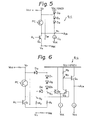
- Fig. 5 which illustrates a third example of the 1-bit memory circuit of Fig. 2, the resistor R 0 of Fig. 4 is deleted, and a diode D 0 is provided on the side of the power supply V CC .
- the operation of the circuit of Fig. 5 is about the same as that of Fig. 4.
- a resistor can be provided instead of the current source I S .
- Fig. 6 which illustrateates a fourth example of the 1-bit memory circuit of Fig. 2, provided between the power supplies V CC and V n is a series circuit formed by three diode stages D 1 , D 2 , and D 3 , and resistors R 1 and R 2 for generating a reference voltage. That is, the potential at node N 1 is the reference voltage which equals determined by the diode stages D 1 , D 2 , and D 3 . Also, in order to determine the potential at node N 2 during a non-broken-mode of the PROM cell PC; a diode D 4 and a resistor R 2 are added to the diodes D 1 , D 2 , and D 3 between the power supplies V CC and V n .
- the potential at node N 2 is determined by the diodes D 1 , D 2 , D 3 , and D 4 . Also, in this case, the potential at node N 2 after a write operation is determined by the diode stage DO and the PROM cell PC.
- the circuit of Fig. 6 during a non-broken-mode of the PROM cell PC,
- Fig. 7 which illustrates a fifth example of the 1-bit memory circuit of Fig. 2, in order to separate the circuit for determining the potential at node N 1 from the circuit for determining the potential at node N 2 during a non-broken-mode, three diode stages D 1 ', D 2 ', and D 3 ' are provided. However, the operation of the circuit of Fig. 7 is the same as that of Fig. 6.
- the potential at node N 2 is increased or decreased by the potential corresponding to one diode stage as compared with the reference voltage at node N, , in accordance with the presence or absence of a write operation (breakdown) of the PROM cell PC.
- the logic amplitude corresponding to one diode stage is read out by the following transistors Q 2 , Q 3 , and Q 4 .
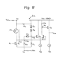
- Fig. 8 which illustrates a sixth example of the 1-bit memory circuit of Fig. 2, the diode D 3 of Fig. 6 is deleted, and a resistor R 0 is provided between the power supplies V CC and Vp. Note that the value of the resistor R 0 is relatively small. Therefore, the potential at node N 1 as the reference voltage is determined by the diodes D 1 and D 2 . The potential at node N 2 during a non-broken-mode of the PROM cell PC is determined by the diodes D 1 , D 2 , and D 4 . The potential at node N 2 after a write mode of the PROM cell PC is -0.8 V determined by the PROM cell PC corresponding to one diode stage. Thus, after a write mode of the PROM cell PC,
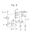
- Fig. 9 which illustrates a seventh example of the 1-bit memory circuit of Fig. 2, the resistor R 0 of Fig. 8 is deleted, and a diode D 0 is provided on the side of the power supply V CC .
- the operation of the circuit of Fig. 9 is about the same as that of Fig. 8.
- Fig. 10 which illustrates an eighth example of the 1-bit memory circuit of Fig. 2, in order to separate the circuit for determining the potential at node N 1 from the circuit for determining the potential at node N 2 , two diode stages D 1 ' and D 2 1 are added. However, the operation of circuit of Fig. 10 is the same as that of Fig. 8.
- the potential at node N 2 is increased or decreased by the potential corresponding to one diode stage as compared with the reference voltage at node N 1 , in accordance with the presence or absence of a write operation (breakdown) of the PROM cell PC.
- the logic amplitude corresponding to one diode stage is read out by the following transistors Q 2 , Q 3 , and Q 4 .
- the output AiR of the circuit of Fig. 3, 4, 5, 6, 7, 8, 9, or 10 is supplied to the address comparing circuit 7 of Fig. 1.
- the address comparing circuit 7 comprises eight exclusive-OR circuits EOR 0 , EOR 1 , ..., EOR 7 , and a NOR circuit NR. That is, when the address signals A 0 , A 1 , ..., and A 7 are completely coincided with the defective address signals A 0R .
- V R is a reference voltage, which is predetermined as suitable for the logic amplitude of the defective address memory circuit 6-i.
- V R is about -2.0 V
- V R is about -1.2 V
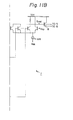
- V RD of Fig. 11 is a predetermined reference voltage.
- the logic amplitude is defined by the number of diode stages, and accordingly, such circuits are helpful in the configuration of the defective address memory circuit for storing a defective address in a bipolar-transistor type RAM having a redundancy configuration.
- each of the row address signals A 0 , A 1 , ..., and A 7 are supplied via emitter-followers Q 11 and Q 12 , diodes D 11 , D 12 , and D 13 , and resistors R 11 and R 12 to the defective address memory circuit 6.
- the high level -0.8 V of the address signals A 0 , A 1 , ..., and A 7 becomes by two stages of the emitter-followers and three stages of the diodes D 11 , D12 , and D 13
- the low level -1.8 V becomes by two stages of the emitter-followers Q 11 and Q 12 and three stages of the diodes.
- the address amplitude of the gates of the write transistors Q 1 is further decreased by resistors R 11 and R 12 .
- Fig. 12 two stages of emitter-followers, three stages of diodes, and the like are used as the level shift down means.
- the number of such stages can be modified as occasion demands or in accordance with the power supply voltage. For example, all the five stages may consist of diodes.
- the write voltage is high, the number of such stages can be more than 6. Further, if the lowest power supply voltage is higher than -5 V, the number of such stages can be less than 4.
Landscapes
- Read Only Memory (AREA)
- Semiconductor Memories (AREA)
Applications Claiming Priority (4)
| Application Number | Priority Date | Filing Date | Title |
|---|---|---|---|
| JP218707/84 | 1984-10-19 | ||
| JP59218707A JPS61100000A (ja) | 1984-10-19 | 1984-10-19 | 情報記憶装置 |
| JP243340/84 | 1984-11-20 | ||
| JP59243340A JPS61123099A (ja) | 1984-11-20 | 1984-11-20 | 半導体記憶装置 |
Publications (3)
| Publication Number | Publication Date |
|---|---|
| EP0178948A2 true EP0178948A2 (fr) | 1986-04-23 |
| EP0178948A3 EP0178948A3 (en) | 1988-01-13 |
| EP0178948B1 EP0178948B1 (fr) | 1991-12-27 |
Family
ID=26522707
Family Applications (1)
| Application Number | Title | Priority Date | Filing Date |
|---|---|---|---|
| EP85307560A Expired - Lifetime EP0178948B1 (fr) | 1984-10-19 | 1985-10-18 | Mémoire à accès aléatoire à transistors bipolaires ayant une configuration à redondance |
Country Status (4)
| Country | Link |
|---|---|
| US (1) | US4744060A (fr) |
| EP (1) | EP0178948B1 (fr) |
| KR (1) | KR900008659B1 (fr) |
| DE (1) | DE3585015D1 (fr) |
Cited By (3)
| Publication number | Priority date | Publication date | Assignee | Title |
|---|---|---|---|---|
| EP0412838A3 (en) * | 1989-08-11 | 1992-01-08 | Sony Corporation | Semiconductor memories |
| EP0419202A3 (en) * | 1989-09-18 | 1992-04-01 | Fujitsu Limited | A semiconductor memory device |
| US5523974A (en) * | 1994-04-25 | 1996-06-04 | Matsushita Electric Industrial Co., Ltd. | Semiconductor memory device with redundant memory cell backup |
Families Citing this family (5)
| Publication number | Priority date | Publication date | Assignee | Title |
|---|---|---|---|---|
| JPH05166396A (ja) * | 1991-12-12 | 1993-07-02 | Mitsubishi Electric Corp | 半導体メモリ装置 |
| JP2741824B2 (ja) * | 1992-10-14 | 1998-04-22 | 三菱電機株式会社 | 半導体記憶装置 |
| GB9305801D0 (en) * | 1993-03-19 | 1993-05-05 | Deans Alexander R | Semiconductor memory system |
| FR2716743B1 (fr) * | 1994-02-28 | 1996-09-27 | Sgs Thomson Microelectronics | Circuit de redondance de mémoire. |
| US7174477B2 (en) * | 2003-02-04 | 2007-02-06 | Micron Technology, Inc. | ROM redundancy in ROM embedded DRAM |
Family Cites Families (5)
| Publication number | Priority date | Publication date | Assignee | Title |
|---|---|---|---|---|
| DE1963895C3 (de) * | 1969-06-21 | 1973-11-29 | Licentia Patent-Verwaltungs-Gmbh, 6000 Frankfurt | Datenspeicher und Datenspeicher anste'uerschaltung |
| JPS5928560Y2 (ja) * | 1979-11-13 | 1984-08-17 | 富士通株式会社 | 冗長ビットを有する記憶装置 |
| JPS5685934A (en) * | 1979-12-14 | 1981-07-13 | Nippon Telegr & Teleph Corp <Ntt> | Control signal generating circuit |
| US4462091A (en) * | 1982-02-26 | 1984-07-24 | International Business Machines Corporation | Word group redundancy scheme |
| JPS595497A (ja) * | 1982-07-02 | 1984-01-12 | Hitachi Ltd | 半導体rom |
-
1985
- 1985-10-17 US US06/788,567 patent/US4744060A/en not_active Expired - Fee Related
- 1985-10-18 KR KR1019850007703A patent/KR900008659B1/ko not_active Expired
- 1985-10-18 DE DE8585307560T patent/DE3585015D1/de not_active Expired - Lifetime
- 1985-10-18 EP EP85307560A patent/EP0178948B1/fr not_active Expired - Lifetime
Cited By (5)
| Publication number | Priority date | Publication date | Assignee | Title |
|---|---|---|---|---|
| EP0412838A3 (en) * | 1989-08-11 | 1992-01-08 | Sony Corporation | Semiconductor memories |
| US5157628A (en) * | 1989-08-11 | 1992-10-20 | Sony Corporation | Semiconductor memory |
| EP0419202A3 (en) * | 1989-09-18 | 1992-04-01 | Fujitsu Limited | A semiconductor memory device |
| US5247476A (en) * | 1989-09-18 | 1993-09-21 | Fujitsu Limited | Semiconductor memory device having a mask rom and a prom |
| US5523974A (en) * | 1994-04-25 | 1996-06-04 | Matsushita Electric Industrial Co., Ltd. | Semiconductor memory device with redundant memory cell backup |
Also Published As
| Publication number | Publication date |
|---|---|
| KR900008659B1 (ko) | 1990-11-26 |
| KR860003665A (ko) | 1986-05-28 |
| EP0178948A3 (en) | 1988-01-13 |
| DE3585015D1 (de) | 1992-02-06 |
| EP0178948B1 (fr) | 1991-12-27 |
| US4744060A (en) | 1988-05-10 |
Similar Documents
| Publication | Publication Date | Title |
|---|---|---|
| US4837747A (en) | Redundary circuit with a spare main decoder responsive to an address of a defective cell in a selected cell block | |
| US4603404A (en) | Semiconductor memory device with redundant cells | |
| KR910000140B1 (ko) | 용장성 회로부를 갖춘 반도체 메모리장치 | |
| US6310806B1 (en) | Semiconductor memory device with redundant circuit | |
| US5502676A (en) | Integrated circuit memory with column redundancy having shared read global data lines | |
| US4745582A (en) | Bipolar-transistor type random access memory device having redundancy configuration | |
| KR900008658B1 (ko) | 용장서 구조를 갖춘 반도체 메모리 장치 | |
| US4385368A (en) | Programmable read only memory | |
| JP3530574B2 (ja) | 半導体記憶装置 | |
| KR100200891B1 (ko) | 반도체 기억장치 | |
| JPH05307898A (ja) | 半導体メモリ装置 | |
| US4587639A (en) | Static semiconductor memory device incorporating redundancy memory cells | |
| JPS63220500A (ja) | 半導体記憶装置の冗長回路 | |
| US5581509A (en) | Double-row address decoding and selection circuitry for an electrically erasable and programmable non-volatile memory device with redundancy, particularly for flash EEPROM devices | |
| US4744060A (en) | Bipolar-transistor type random access memory having redundancy configuration | |
| US4987560A (en) | Semiconductor memory device | |
| US4347585A (en) | Reproduce only storage matrix | |
| US4996670A (en) | Zero standby power, radiation hardened, memory redundancy circuit | |
| EP0053504A2 (fr) | Mémoire statique semi-conductrice | |
| US5390150A (en) | Semiconductor memory device with redundancy structure suppressing power consumption | |
| US5058070A (en) | High speed memory with row redundancy | |
| US4724341A (en) | CMOS decoder circuit resistant to latch-up | |
| US4722822A (en) | Column-current multiplexing driver circuit for high density proms | |
| US6982912B2 (en) | Semiconductor memory device | |
| EP0098142A2 (fr) | Dispositifs de mémoire morte programmables |
Legal Events
| Date | Code | Title | Description |
|---|---|---|---|
| PUAI | Public reference made under article 153(3) epc to a published international application that has entered the european phase |
Free format text: ORIGINAL CODE: 0009012 |
|
| AK | Designated contracting states |
Kind code of ref document: A2 Designated state(s): DE FR GB |
|
| PUAL | Search report despatched |
Free format text: ORIGINAL CODE: 0009013 |
|
| AK | Designated contracting states |
Kind code of ref document: A3 Designated state(s): DE FR GB |
|
| 17P | Request for examination filed |
Effective date: 19880617 |
|
| 17Q | First examination report despatched |
Effective date: 19891124 |
|
| GRAA | (expected) grant |
Free format text: ORIGINAL CODE: 0009210 |
|
| AK | Designated contracting states |
Kind code of ref document: B1 Designated state(s): DE FR GB |
|
| REF | Corresponds to: |
Ref document number: 3585015 Country of ref document: DE Date of ref document: 19920206 |
|
| ET | Fr: translation filed | ||
| PLBE | No opposition filed within time limit |
Free format text: ORIGINAL CODE: 0009261 |
|
| STAA | Information on the status of an ep patent application or granted ep patent |
Free format text: STATUS: NO OPPOSITION FILED WITHIN TIME LIMIT |
|
| 26N | No opposition filed | ||
| PGFP | Annual fee paid to national office [announced via postgrant information from national office to epo] |
Ref country code: GB Payment date: 19941010 Year of fee payment: 10 Ref country code: DE Payment date: 19941010 Year of fee payment: 10 |
|
| PGFP | Annual fee paid to national office [announced via postgrant information from national office to epo] |
Ref country code: FR Payment date: 19941011 Year of fee payment: 10 |
|
| PG25 | Lapsed in a contracting state [announced via postgrant information from national office to epo] |
Ref country code: GB Effective date: 19951018 |
|
| GBPC | Gb: european patent ceased through non-payment of renewal fee |
Effective date: 19951018 |
|
| PG25 | Lapsed in a contracting state [announced via postgrant information from national office to epo] |
Ref country code: FR Effective date: 19960628 |
|
| PG25 | Lapsed in a contracting state [announced via postgrant information from national office to epo] |
Ref country code: DE Effective date: 19960702 |
|
| REG | Reference to a national code |
Ref country code: FR Ref legal event code: ST |