EP0180780A1 - Testeur dynamique sans contacts pour circuits intégrés - Google Patents
Testeur dynamique sans contacts pour circuits intégrés Download PDFInfo
- Publication number
- EP0180780A1 EP0180780A1 EP85112610A EP85112610A EP0180780A1 EP 0180780 A1 EP0180780 A1 EP 0180780A1 EP 85112610 A EP85112610 A EP 85112610A EP 85112610 A EP85112610 A EP 85112610A EP 0180780 A1 EP0180780 A1 EP 0180780A1
- Authority
- EP
- European Patent Office
- Prior art keywords
- laser
- integrated circuit
- test chip
- test
- energy
- Prior art date
- Legal status (The legal status is an assumption and is not a legal conclusion. Google has not performed a legal analysis and makes no representation as to the accuracy of the status listed.)
- Granted
Links
- 238000012360 testing method Methods 0.000 claims abstract description 69
- 238000000034 method Methods 0.000 claims abstract description 33
- 238000001514 detection method Methods 0.000 claims abstract description 18
- 230000008569 process Effects 0.000 claims abstract description 13
- 239000002131 composite material Substances 0.000 claims abstract description 12
- 239000000543 intermediate Substances 0.000 claims abstract description 12
- 230000004048 modification Effects 0.000 claims abstract description 7
- 238000012986 modification Methods 0.000 claims abstract description 7
- 230000035945 sensitivity Effects 0.000 claims description 6
- 230000000979 retarding effect Effects 0.000 claims description 4
- 230000005855 radiation Effects 0.000 claims description 3
- 229910001220 stainless steel Inorganic materials 0.000 claims description 3
- 239000010935 stainless steel Substances 0.000 claims description 3
- 230000005684 electric field Effects 0.000 claims description 2
- 230000003247 decreasing effect Effects 0.000 claims 1
- 238000004519 manufacturing process Methods 0.000 abstract description 5
- 235000012431 wafers Nutrition 0.000 abstract description 4
- 238000006243 chemical reaction Methods 0.000 abstract 1
- 238000012544 monitoring process Methods 0.000 description 8
- 239000000523 sample Substances 0.000 description 7
- 239000004065 semiconductor Substances 0.000 description 7
- 238000010586 diagram Methods 0.000 description 5
- 230000008859 change Effects 0.000 description 4
- 239000013078 crystal Substances 0.000 description 4
- 239000000463 material Substances 0.000 description 4
- 238000005259 measurement Methods 0.000 description 4
- 230000003287 optical effect Effects 0.000 description 4
- 230000004936 stimulating effect Effects 0.000 description 4
- 230000008901 benefit Effects 0.000 description 3
- 238000009826 distribution Methods 0.000 description 3
- OKTJSMMVPCPJKN-UHFFFAOYSA-N Carbon Chemical compound [C] OKTJSMMVPCPJKN-UHFFFAOYSA-N 0.000 description 2
- 238000001069 Raman spectroscopy Methods 0.000 description 2
- 238000004458 analytical method Methods 0.000 description 2
- XKRFYHLGVUSROY-UHFFFAOYSA-N argon Substances [Ar] XKRFYHLGVUSROY-UHFFFAOYSA-N 0.000 description 2
- 229910052786 argon Inorganic materials 0.000 description 2
- 229910003460 diamond Inorganic materials 0.000 description 2
- 239000010432 diamond Substances 0.000 description 2
- 230000007246 mechanism Effects 0.000 description 2
- 238000001259 photo etching Methods 0.000 description 2
- 229920000728 polyester Polymers 0.000 description 2
- 238000001228 spectrum Methods 0.000 description 2
- 238000010897 surface acoustic wave method Methods 0.000 description 2
- 230000001052 transient effect Effects 0.000 description 2
- XUIMIQQOPSSXEZ-UHFFFAOYSA-N Silicon Chemical compound [Si] XUIMIQQOPSSXEZ-UHFFFAOYSA-N 0.000 description 1
- 229910000831 Steel Inorganic materials 0.000 description 1
- 229910052782 aluminium Inorganic materials 0.000 description 1
- XAGFODPZIPBFFR-UHFFFAOYSA-N aluminium Chemical compound [Al] XAGFODPZIPBFFR-UHFFFAOYSA-N 0.000 description 1
- 238000013459 approach Methods 0.000 description 1
- QVGXLLKOCUKJST-UHFFFAOYSA-N atomic oxygen Chemical compound [O] QVGXLLKOCUKJST-UHFFFAOYSA-N 0.000 description 1
- 230000005540 biological transmission Effects 0.000 description 1
- 229910052799 carbon Inorganic materials 0.000 description 1
- 239000002800 charge carrier Substances 0.000 description 1
- 230000001427 coherent effect Effects 0.000 description 1
- 150000001875 compounds Chemical class 0.000 description 1
- 238000000151 deposition Methods 0.000 description 1
- 230000008021 deposition Effects 0.000 description 1
- 230000007613 environmental effect Effects 0.000 description 1
- 230000004907 flux Effects 0.000 description 1
- 229910002804 graphite Inorganic materials 0.000 description 1
- 239000010439 graphite Substances 0.000 description 1
- 238000005286 illumination Methods 0.000 description 1
- 238000011065 in-situ storage Methods 0.000 description 1
- 238000009413 insulation Methods 0.000 description 1
- 238000005224 laser annealing Methods 0.000 description 1
- 230000031700 light absorption Effects 0.000 description 1
- 229910052751 metal Inorganic materials 0.000 description 1
- 239000002184 metal Substances 0.000 description 1
- 238000001465 metallisation Methods 0.000 description 1
- 239000001301 oxygen Substances 0.000 description 1
- 229910052760 oxygen Inorganic materials 0.000 description 1
- 238000002161 passivation Methods 0.000 description 1
- 238000012545 processing Methods 0.000 description 1
- 239000010453 quartz Substances 0.000 description 1
- 229910052594 sapphire Inorganic materials 0.000 description 1
- 239000010980 sapphire Substances 0.000 description 1
- 229910052710 silicon Inorganic materials 0.000 description 1
- 239000010703 silicon Substances 0.000 description 1
- VYPSYNLAJGMNEJ-UHFFFAOYSA-N silicon dioxide Inorganic materials O=[Si]=O VYPSYNLAJGMNEJ-UHFFFAOYSA-N 0.000 description 1
- 238000004088 simulation Methods 0.000 description 1
- 239000010959 steel Substances 0.000 description 1
- 230000000638 stimulation Effects 0.000 description 1
- 239000000758 substrate Substances 0.000 description 1
- 239000010409 thin film Substances 0.000 description 1
- 230000007704 transition Effects 0.000 description 1
Images
Classifications
-
- G—PHYSICS
- G01—MEASURING; TESTING
- G01R—MEASURING ELECTRIC VARIABLES; MEASURING MAGNETIC VARIABLES
- G01R31/00—Arrangements for testing electric properties; Arrangements for locating electric faults; Arrangements for electrical testing characterised by what is being tested not provided for elsewhere
- G01R31/28—Testing of electronic circuits, e.g. by signal tracer
- G01R31/302—Contactless testing
- G01R31/308—Contactless testing using non-ionising electromagnetic radiation, e.g. optical radiation
Definitions
- This invention relates to integrated circuits testing, and more particularly to a nonintrusive noncontact dynamic testing technique using a pulsed laser to excite electron emissions as a function of dynamic operation of the circuit and to detect those emissions by an adjacent detector without the need for ohmic contacts or special circuitry on the integrated circuit chip or wafer.
- a common way of testing an electronic circuit is a dynamic view of the circuit, voltage or currents, in operation, by means of an oscilloscope.
- the engineer probes the circuit at various test probe positions, for example by pricking certain landing pads with the points of test probes to make good contact, and views the resulting electrical conditions via analogous traces on the oscilloscope viewing tube.
- circuits have become more compact and complex, it has become more and more difficult to accomplish nonin- trus i ve positioning of test probe points without the danger of destroying the circuit, or at least of providing such a relatively enormous change due to the physical mass of the probes that the test becomes suspect.
- a totally nonintrusive contactless oscilloscope is a known desire.
- the contactless oscilloscope is the e-beam tester, but the e-beam is somewhat intrusive in that the high energy (100 electron volts or more) of the incident electrons may cause permanent material damage where the e-beam strikes the surface being tested.
- Iwamoto et al shows an apparatus for determing the average size of fundamental patterns by comparing Fourier transforms of pattern images in a processor and providing the patterns by applying coherent light focused on a target for test and monitoring the reflected images by converting them to Fourier transforms and comparing the Fourier transforms against known image patterns. This is a contactless optical technique for image recognition; it is not a currentvoltage tester.
- Henley "Logic Failure Analysis of CMOS Using a Laser Probe," Spectrum Sciences, 3050 Oakmead Village Drive, Santa Clara, California, 95051, shows a laser contactless probe for an integrated circuit, using available pin connections to conduct stimulated current-voltage signals to a computer for analysis. Henley does not use an adjacent detector, but must dedicate a certain amount of circuitry (external to the integrated circuit under test) to the conduction of test signals. No photoemission from the circuit is created.
- the logic state of the integrated circuit is determined by interrupting its dynamic operation and then measuring the current transient induced in the power supply by laser light absorption in an active semiconductor region (the light does not impinge on the metal wires and nodes of the circuit); as a result, neither logic states nor AC switching waveforms are determined during dynamic operation of the circuit.
- the prior art does not teach nor suggest the invention, the technique of stimulating electron emission signals in an integrated circuit by the use of a pulsed laser for accurate time-resolution, without actual contact, by focussing a modified laser beam on a portion of the integrated circuit while in operation with signal dynamics, and monitoring those emissions for test against oppropriate norms, to determine whether the integrated circuit is operating property.
- a modified pulsed laser beam is focussed on a node of the integrated circuit under test while under operation with signal dynamics, and monitoring those emissions for test against appropriate norms.
- a feature of the invention is its operation as a nonintrusive probeless oscilloscope, with time resolution on the order of 5 picoseconds, and thus with ability to measure AC switching transients during change in logic states, as well as logic states themselves for most advanced high speed circuits.
- An advantage of the invention is that it operates without requiring human dexterity, with great precision, and without damage to the integrated circuit under test.
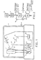
- Fig. 1 is a schematic diagram of the contactless tester for integrated circuit process intermediates, which may include wafers, dice or chips in various stages of manufacture. These process intermediates may be simple or may be complex; it is common to have complex semiconductor doping areas embedded in a silicon substrate, covered with several layers of metallization interspersed with several layers of insulation or passivation. For ease of discussion, all such integrated circuit process intermediates will be identified merely as "test chip".
- the test chip 1 is mounted in a suitable mounting means 2 which provides connections for dynamic signals simulation operation and does not obscure passage of light to contact pads such as pad 3.
- the entire operation is carried out in an environmental changer 4 which provides appropriate operating environment vacuum for the integrated circuit test.
- Test chip 1 is supplied with suitable bias voltages from bias source 5 and is supplied with appropriate dynamic operating signals from signal generator and test computer 6.
- Bias source 5 is shown in Fig. 1 as a variable battery; in practice, it may be a computer controlled variable voltage supply such as a number of different voltage supplies separately gated by the computer 6. Bias source 5, under computer control, thus can provide operating bias voltage or an off-specification bias voltage to simulate stressed operation.
- Signal generator and test computer 6 is equipped to provide an appropriate dynamic exercise to test chip 1 so as to facilitate the test at the operating speed for which the circuit normally is run.
- the test chip 1 can also be dynamically stressed by high speed or off specification voltages, currents or timings.
- test chip 1 has been exercised to the point of operating temperature and to the point where a signal of known characteristics is expected at pad 3, it is desired to determine whether the appropriate signal is present or not.
- Laser 7 with laser light modulation mechanism 8 and focusing mechanism 9 applies a focused laser beam of appropriate characteristics focused upon pad 3 in such a manner that pad 3 emits signal modulated electron emissions 10 as a composite function of the applied laser light and the integrated circuit signal available at pad 3 at the instant of the test.
- Emissions 10 pass through detector bias means (grid 11 and bias source 12 shown) and if of appropriate signal characteristics pass the detector bias means to detector 13.
- Bias source 12 is shown in Fig.
- bias source 12 may take a variety of forms, so long as the detector bias is appropriate to the detector and to the test being performed.
- the detection means comprises a retarding electric field, through which the electrons pass, such that only those electrons with energies above a critical value (for example, 1 eV for a 1 eV retarding voltage difference between detector system and chip test point) reach the detector system and are measured.
- the preferred detector system includes detector 13, collector 14 and counter 15.
- Detector 13 is a channel electron multiplier or other electron signal measuring detector which supplies electrons via collector 14 to electron counting circuit 15.
- a suitable electron multiplier is Galileo Electrooptics 4219 or 4730, for example.
- the electron multiplier, associated electron collector and pulse discrimination counter or current measuring amplifier together form detector means.
- a suitable electron collector may be simply a piece of stainless ' steel sheet formed into a dish, or a "last dynode" or electrode connected to a current mea- surer. Electron counts are fed back to the test signal generator 6 for comparison against appropriate test norms and determination of test results for use in further testing acceptance or rejection of integrated circuit 1.
- Fig. 2 is a schematic diagram of the laser modification technique used to provide focused light for stimulating signal modulated emissions as a function of signal dynamics in the integrated circuit under test.
- Laser 7 in Fig. 1 preferably is a composite laser having a first stage 16 which is a CW pumped laser (argon ion, or YAG) and having a second stage 17 which is a mode-locked dye laser.
- the composite laser provides an output of collimated light at 6600A (1.88 eV) with a nominal 5 psec pulser width and a nominal 1 Mhz repetition rate.
- Second harmonic generating crystal 22 produces 3.76 eV photons by combining 1.88 eV photons two at a time. To these 3.76 eV photons more 1.88 eV photons are combined (using the mirror system 18-21 with mirror 18 being semitransparent) in third harmonic generating crystal 23, producing 5.64 eV photons from combinations of 3.76 and 1.88 eV photons.
- the resulting high energy laser photons (5.64 eV in this case) have sufficient energy to excite the photoelectron emission during the nominal 5 psec pulse width of the laser pulses, so that the emission carries direct information on the voltage state of the pad 3 (Fig. 1) during the very short laser pulse.
- the voltage and switching behaviour of pad 3 during circuit operation is determined.
- repetition and measurement rates of nominal 1 Mhz are achieved.
- the laser photon flux from such a system is 2x10 6 photons/pulse.
- This light signal is appropriate to provide signal modulated emissions 10, Fig. 1, as a composite function of the focused laser beam and the signal dynamics. in operation of integrated circuit 1 as expessed by signal at pad 3.
- Lens 9, grid 11, detector 13, collector 14, and counter 15 are:
- signal detector and test computer 6 are those of a high speed logic testing system, of any type now common to the art of testing an integrated circuit by exercising it under dynamic conditions simulating actual or stressed operation.
- the operating environment within chamber 4 is vacuum with approximately 10- 5 , 10- 6 torr base -pressure (or lower).
- the electron emission signal 10 caused by the laser pulse carries a characteristic distribution of electron energies.
- the emission signal 10 as measured by the detection system consisting of grind system 11, 12 and detection system 13-15 reflects the voltage at pad 3 during the laser pulse, which can be sufficiently fast for example, nominal 5 picoseconds for very high speed circuits, to resolve the AC switching transient accompanying a change in logic state of pad 3 (as well as the logic state itself).
- Grid 11 may in certain situations be eliminated; without the grind the front surface of detector 13 functions as bias means in that the voltage between pad 3 and detector 13 determines the number of electrons arriving at detector 13.
- detection systems are sensitive to both the primary (directly ejected) photoelectrons and resulting secondary electrons, energy distributions of which are illustrated in the photoemission diagram in Rubloff, IBM Technical Disclosure Bulletin, Vol. 25, p. 1171, 1982.
- enhanced sensitivity may be achieved by choosing the laser photon energy for the selected material of the test pad, typically aluminum, to be close to the photoelectron emission threshold.
- An alternative detection system is a bandpass electron energy analyzer which detects only electrons arriving at the analyzer with a specific energy.
- sensitivity advantages may accrue by choosing the laser photon energy notable above the photoelectron emission threshold (for example. 1-2 eV above).
- the sensitivity is enhanced by preferential measurement of electrons at the transitions (thresholds) of the secondary and primary electron energy distribution spectra.
- composite pulsed laser system may also be used. These may include, for example, Raman shift lasers (using stimulated Raman scattering to change photon energy); frequency mixing laser systems (more general than harmonic generation); excimer laser systems, dye laser systems, second harmonic generation (without third harmonic generation), and others.
- Raman shift lasers using stimulated Raman scattering to change photon energy
- frequency mixing laser systems more general than harmonic generation
- excimer laser systems dye laser systems, second harmonic generation (without third harmonic generation), and others.
Landscapes
- Physics & Mathematics (AREA)
- Engineering & Computer Science (AREA)
- Health & Medical Sciences (AREA)
- Computer Vision & Pattern Recognition (AREA)
- Electromagnetism (AREA)
- Toxicology (AREA)
- General Engineering & Computer Science (AREA)
- General Physics & Mathematics (AREA)
- Tests Of Electronic Circuits (AREA)
- Testing Or Measuring Of Semiconductors Or The Like (AREA)
Applications Claiming Priority (2)
| Application Number | Priority Date | Filing Date | Title |
|---|---|---|---|
| US667506 | 1984-11-01 | ||
| US06/667,506 US4706018A (en) | 1984-11-01 | 1984-11-01 | Noncontact dynamic tester for integrated circuits |
Publications (2)
| Publication Number | Publication Date |
|---|---|
| EP0180780A1 true EP0180780A1 (fr) | 1986-05-14 |
| EP0180780B1 EP0180780B1 (fr) | 1989-09-27 |
Family
ID=24678500
Family Applications (1)
| Application Number | Title | Priority Date | Filing Date |
|---|---|---|---|
| EP85112610A Expired EP0180780B1 (fr) | 1984-11-01 | 1985-10-04 | Testeur dynamique sans contacts pour circuits intégrés |
Country Status (5)
| Country | Link |
|---|---|
| US (1) | US4706018A (fr) |
| EP (1) | EP0180780B1 (fr) |
| JP (1) | JPS61108148A (fr) |
| CA (1) | CA1220559A (fr) |
| DE (1) | DE3573320D1 (fr) |
Cited By (5)
| Publication number | Priority date | Publication date | Assignee | Title |
|---|---|---|---|---|
| WO1987007028A3 (fr) * | 1986-05-16 | 1987-12-17 | Bell Communications Res | Sonde laser a haute vitesse |
| EP0264481A1 (fr) * | 1986-10-23 | 1988-04-27 | International Business Machines Corporation | Procédé de test dans le vide pour substrats de circuits intégrés employant un laser |
| EP0326858A1 (fr) * | 1988-01-28 | 1989-08-09 | Siemens Aktiengesellschaft | Procédé et appareil pour visualiser des signaux périodiques avec une sonde de laser |
| EP0694961B1 (fr) * | 1994-07-29 | 2001-10-17 | Nec Corporation | Procédé et appareil pour détecter un point de court-circuit entre des schémas conducteurs |
| FR2923021A1 (fr) * | 2007-10-26 | 2009-05-01 | Eads Europ Aeronautic Defence | Procede de determination de la sensibilite des composants electroniques vis-a-vis des particules. |
Families Citing this family (17)
| Publication number | Priority date | Publication date | Assignee | Title |
|---|---|---|---|---|
| EP0404970A1 (fr) * | 1989-06-26 | 1991-01-02 | International Business Machines Corporation | Procédé et dispositif pour le test sans contact d'activité électronique d'un circuit intégré à tester après sa passivation |
| US6525555B1 (en) * | 1993-11-16 | 2003-02-25 | Formfactor, Inc. | Wafer-level burn-in and test |
| US6472889B1 (en) | 2000-06-15 | 2002-10-29 | University Of Connecticut | Apparatus and method for producing an ion channel microprobe |
| US6891363B2 (en) * | 2002-09-03 | 2005-05-10 | Credence Systems Corporation | Apparatus and method for detecting photon emissions from transistors |
| US6943572B2 (en) * | 2002-09-03 | 2005-09-13 | Credence Systems Corporation | Apparatus and method for detecting photon emissions from transistors |
| KR100613169B1 (ko) * | 2004-10-12 | 2006-08-17 | 삼성전자주식회사 | 무접촉 반도체 소자 테스트 장치 및 테스트 방법 |
| US7202689B2 (en) * | 2005-04-15 | 2007-04-10 | International Business Machines Corporation | Sensor differentiated fault isolation |
| US7888955B2 (en) * | 2007-09-25 | 2011-02-15 | Formfactor, Inc. | Method and apparatus for testing devices using serially controlled resources |
| US7977959B2 (en) * | 2007-09-27 | 2011-07-12 | Formfactor, Inc. | Method and apparatus for testing devices using serially controlled intelligent switches |
| US7623982B2 (en) * | 2007-11-05 | 2009-11-24 | Semicaps Pte Ltd | Method of testing an electronic circuit and apparatus thereof |
| US20090164931A1 (en) * | 2007-12-19 | 2009-06-25 | Formfactor, Inc. | Method and Apparatus for Managing Test Result Data Generated by a Semiconductor Test System |
| US20090224793A1 (en) * | 2008-03-07 | 2009-09-10 | Formfactor, Inc. | Method And Apparatus For Designing A Custom Test System |
| US8122309B2 (en) * | 2008-03-11 | 2012-02-21 | Formfactor, Inc. | Method and apparatus for processing failures during semiconductor device testing |
| US8095841B2 (en) * | 2008-08-19 | 2012-01-10 | Formfactor, Inc. | Method and apparatus for testing semiconductor devices with autonomous expected value generation |
| US7944225B2 (en) | 2008-09-26 | 2011-05-17 | Formfactor, Inc. | Method and apparatus for providing a tester integrated circuit for testing a semiconductor device under test |
| FR2992067A1 (fr) * | 2012-06-13 | 2013-12-20 | St Microelectronics Grenoble 2 | Procede et dispositif d'ajustement de la tension de polarisation d'une photodiode spad |
| US10139358B2 (en) * | 2016-01-11 | 2018-11-27 | International Business Machines Corporation | Method for characterization of a layered structure |
Citations (1)
| Publication number | Priority date | Publication date | Assignee | Title |
|---|---|---|---|---|
| EP0129508A1 (fr) * | 1983-05-25 | 1984-12-27 | Battelle Memorial Institute | Procédé d'examen et de test d'un dispositif électrique du type des circuits intégrés ou imprimés |
Family Cites Families (9)
| Publication number | Priority date | Publication date | Assignee | Title |
|---|---|---|---|---|
| US3129353A (en) * | 1960-05-17 | 1964-04-14 | Mrs Jennings | Multiple radiation source microscope |
| US3370168A (en) * | 1964-01-14 | 1968-02-20 | Hitachi Ltd | Anode aperture plate for a television camera tube in an electron microscope comprising a stainless steel foil |
| JPS522573A (en) * | 1975-06-24 | 1977-01-10 | Toshiba Corp | Surface potential measuring device |
| US4266138A (en) * | 1978-07-11 | 1981-05-05 | Cornell Research Foundation, Inc. | Diamond targets for producing high intensity soft x-rays and a method of exposing x-ray resists |
| US4332833A (en) * | 1980-02-29 | 1982-06-01 | Bell Telephone Laboratories, Incorporated | Method for optical monitoring in materials fabrication |
| JPS56124003A (en) * | 1980-03-06 | 1981-09-29 | Toshiba Corp | Measuring device for pattern |
| US4380864A (en) * | 1981-07-27 | 1983-04-26 | The United States Of America As Represented By The Secretary Of The Air Force | Method for providing in-situ non-destructive monitoring of semiconductors during laser annealing process |
| US4417948A (en) * | 1982-07-09 | 1983-11-29 | International Business Machines Corporation | Self developing, photoetching of polyesters by far UV radiation |
| JPS59141238A (ja) * | 1983-02-01 | 1984-08-13 | Hitachi Ltd | キヤリア寿命測定装置 |
-
1984
- 1984-11-01 US US06/667,506 patent/US4706018A/en not_active Expired - Fee Related
-
1985
- 1985-05-23 CA CA000482173A patent/CA1220559A/fr not_active Expired
- 1985-08-14 JP JP60177789A patent/JPS61108148A/ja active Pending
- 1985-10-04 EP EP85112610A patent/EP0180780B1/fr not_active Expired
- 1985-10-04 DE DE8585112610T patent/DE3573320D1/de not_active Expired
Patent Citations (1)
| Publication number | Priority date | Publication date | Assignee | Title |
|---|---|---|---|---|
| EP0129508A1 (fr) * | 1983-05-25 | 1984-12-27 | Battelle Memorial Institute | Procédé d'examen et de test d'un dispositif électrique du type des circuits intégrés ou imprimés |
Non-Patent Citations (4)
| Title |
|---|
| FUJITSU-SCIENTIFIC & TECHNICAL JOURNAL, vol. 19, no. 4, 1983, pages 431-441, Kawasaki, JP; A. ITO et al.: "Hemispherical retarding type energy analyzer for LSI testing by an electron beam" * |
| IBM TECHNICAL DISCLOSURE BULLETIN, vol. 25, no. 3A, August 1982, pages 1171-1172, New York, US; G.W. RUBLOFF: "Contactless measurement of voltage levels using photoemission" * |
| MICROELECTRONICS JOURNAL, vol. 11, no. 2, March/April 1980, pages 35-40, Mackintosh Publications Ltd., Luton, GB; C.E. JOWETT: "Surface analytical techniques applied to electronic components" * |
| REV. SCIENTIFIC INSTRUMENTS, vol. 49, no. 6, June 1978, page 756-759, American Institute of Physics, New York, US; M. KUDO et al.: "Computer controlled ESCA for nondestructive surface characterization utilizing a TV-type position sensitive detector" * |
Cited By (11)
| Publication number | Priority date | Publication date | Assignee | Title |
|---|---|---|---|---|
| WO1987007028A3 (fr) * | 1986-05-16 | 1987-12-17 | Bell Communications Res | Sonde laser a haute vitesse |
| EP0264481A1 (fr) * | 1986-10-23 | 1988-04-27 | International Business Machines Corporation | Procédé de test dans le vide pour substrats de circuits intégrés employant un laser |
| US4843329A (en) * | 1986-10-23 | 1989-06-27 | International Business Machines Corporation | Method for contactless testing for electrical opens and short circuits in conducting paths in a substrate |
| EP0326858A1 (fr) * | 1988-01-28 | 1989-08-09 | Siemens Aktiengesellschaft | Procédé et appareil pour visualiser des signaux périodiques avec une sonde de laser |
| US4902963A (en) * | 1988-01-28 | 1990-02-20 | Brust Hans D | Method and arrangement for recording periodic signals with a laser probe |
| EP0694961B1 (fr) * | 1994-07-29 | 2001-10-17 | Nec Corporation | Procédé et appareil pour détecter un point de court-circuit entre des schémas conducteurs |
| FR2923021A1 (fr) * | 2007-10-26 | 2009-05-01 | Eads Europ Aeronautic Defence | Procede de determination de la sensibilite des composants electroniques vis-a-vis des particules. |
| WO2009056738A1 (fr) * | 2007-10-26 | 2009-05-07 | European Aeronautic Defence And Space Company Eads France | Procede de determination de la sensibilite des composants electroniques vis a vis des particules |
| CN101910855A (zh) * | 2007-10-26 | 2010-12-08 | 欧洲航空防务与空间公司Eads法国 | 确定电子部件对粒子的敏感度的方法 |
| US8577662B2 (en) | 2007-10-26 | 2013-11-05 | European Aeronautic Defence And Space Company Eads France | Method of determining the particle sensitivity of electronic components |
| CN101910855B (zh) * | 2007-10-26 | 2014-03-26 | 欧洲航空防务与空间公司Eads法国 | 确定电子部件对粒子的敏感度的方法 |
Also Published As
| Publication number | Publication date |
|---|---|
| JPS61108148A (ja) | 1986-05-26 |
| US4706018A (en) | 1987-11-10 |
| EP0180780B1 (fr) | 1989-09-27 |
| DE3573320D1 (en) | 1989-11-02 |
| CA1220559A (fr) | 1987-04-14 |
Similar Documents
| Publication | Publication Date | Title |
|---|---|---|
| EP0180780B1 (fr) | Testeur dynamique sans contacts pour circuits intégrés | |
| EP0216077B1 (fr) | Appareil de test pour circuits intégrés dans leur ensemble | |
| Habing | The use of lasers to simulate radiation-induced transients in semiconductor devices and circuits | |
| US4816753A (en) | Method for reliability testing of integrated circuits | |
| US5017863A (en) | Electro-emissive laser stimulated test | |
| TWI823125B (zh) | 帶電粒子束裝置及相關的非暫時性電腦可讀媒體 | |
| US4786865A (en) | Method and apparatus for testing integrated circuit susceptibility to cosmic rays | |
| Kania et al. | Absolute x‐ray power measurements with subnanosecond time resolution using type IIa diamond photoconductors | |
| Pease et al. | Comparison of SETs in bipolar linear circuits generated with an ion microbeam, laser light, and circuit simulation | |
| US7019311B1 (en) | Laser-based irradiation apparatus and methods for monitoring the dose-rate response of semiconductor devices | |
| US4644264A (en) | Photon assisted tunneling testing of passivated integrated circuits | |
| US5331161A (en) | Ion irradiation system and method | |
| US4845425A (en) | Full chip integrated circuit tester | |
| US4786864A (en) | Photon assisted tunneling testing of passivated integrated circuits | |
| Naylor et al. | A sub-picosecond accumulating streak camera for x-rays | |
| King et al. | Transient radiation screening of silicon devices using backside laser irradiation | |
| US5030909A (en) | Method and system for contactless testing of electronic activity in an integrated circuit chip-to-test after passivation thereof | |
| Pocaterra et al. | Single event burnout failures caused in silicon carbide power devices by alpha particles emitted from radionuclides | |
| Kamiya et al. | High energy single ion hit system combined with heavy ion microbeam apparatus | |
| JPH0573579U (ja) | 集積回路製造時の中間体の動的テスト装置 | |
| Seitz et al. | Energy and time-resolved photoemission in a promising new approach for contactless integrated-circuit testing | |
| Nikiforov et al. | " RADON-5E" portable pulsed laser simulator: description, qualification technique and results, dosimetry procedure | |
| Antonelli et al. | Bunch by bunch beam monitoring in 3rd and 4th generation light sources by means of single crystal diamond detectors and quantum well devices | |
| US4724536A (en) | Instrument to measure fluorescence which has occurred in a sample stimulated by X rays | |
| US4166218A (en) | P-i-n diode detector of ionizing radiation with electric field straightening |
Legal Events
| Date | Code | Title | Description |
|---|---|---|---|
| PUAI | Public reference made under article 153(3) epc to a published international application that has entered the european phase |
Free format text: ORIGINAL CODE: 0009012 |
|
| AK | Designated contracting states |
Kind code of ref document: A1 Designated state(s): DE FR GB |
|
| 17P | Request for examination filed |
Effective date: 19860919 |
|
| 17Q | First examination report despatched |
Effective date: 19880725 |
|
| GRAA | (expected) grant |
Free format text: ORIGINAL CODE: 0009210 |
|
| AK | Designated contracting states |
Kind code of ref document: B1 Designated state(s): DE FR GB |
|
| REF | Corresponds to: |
Ref document number: 3573320 Country of ref document: DE Date of ref document: 19891102 |
|
| ET | Fr: translation filed | ||
| PLBE | No opposition filed within time limit |
Free format text: ORIGINAL CODE: 0009261 |
|
| STAA | Information on the status of an ep patent application or granted ep patent |
Free format text: STATUS: NO OPPOSITION FILED WITHIN TIME LIMIT |
|
| 26N | No opposition filed | ||
| PGFP | Annual fee paid to national office [announced via postgrant information from national office to epo] |
Ref country code: FR Payment date: 19951009 Year of fee payment: 11 |
|
| PGFP | Annual fee paid to national office [announced via postgrant information from national office to epo] |
Ref country code: DE Payment date: 19951030 Year of fee payment: 11 |
|
| PGFP | Annual fee paid to national office [announced via postgrant information from national office to epo] |
Ref country code: GB Payment date: 19960925 Year of fee payment: 12 |
|
| PG25 | Lapsed in a contracting state [announced via postgrant information from national office to epo] |
Ref country code: FR Effective date: 19970630 |
|
| PG25 | Lapsed in a contracting state [announced via postgrant information from national office to epo] |
Ref country code: DE Effective date: 19970701 |
|
| REG | Reference to a national code |
Ref country code: FR Ref legal event code: ST |
|
| PG25 | Lapsed in a contracting state [announced via postgrant information from national office to epo] |
Ref country code: GB Free format text: LAPSE BECAUSE OF NON-PAYMENT OF DUE FEES Effective date: 19971004 |
|
| GBPC | Gb: european patent ceased through non-payment of renewal fee |
Effective date: 19971004 |