EP0181507A1 - Vorrichtung zur Aufzeichnung eines Bildes mittels eines Elektronenmikroskops - Google Patents
Vorrichtung zur Aufzeichnung eines Bildes mittels eines Elektronenmikroskops Download PDFInfo
- Publication number
- EP0181507A1 EP0181507A1 EP85112937A EP85112937A EP0181507A1 EP 0181507 A1 EP0181507 A1 EP 0181507A1 EP 85112937 A EP85112937 A EP 85112937A EP 85112937 A EP85112937 A EP 85112937A EP 0181507 A1 EP0181507 A1 EP 0181507A1
- Authority
- EP
- European Patent Office
- Prior art keywords
- sensor
- image
- dimensional
- recorder
- stimulable phosphor
- Prior art date
- Legal status (The legal status is an assumption and is not a legal conclusion. Google has not performed a legal analysis and makes no representation as to the accuracy of the status listed.)
- Granted
Links
- OAICVXFJPJFONN-UHFFFAOYSA-N Phosphorus Chemical compound [P] OAICVXFJPJFONN-UHFFFAOYSA-N 0.000 claims abstract description 105
- 238000010894 electron beam technology Methods 0.000 claims abstract description 33
- 230000005855 radiation Effects 0.000 claims description 22
- 230000015572 biosynthetic process Effects 0.000 claims description 6
- 238000010438 heat treatment Methods 0.000 claims description 3
- 230000001678 irradiating effect Effects 0.000 claims description 2
- 238000004804 winding Methods 0.000 claims 2
- 238000001000 micrograph Methods 0.000 abstract description 30
- 239000000203 mixture Substances 0.000 description 16
- 229910052794 bromium Inorganic materials 0.000 description 15
- 229910052801 chlorine Inorganic materials 0.000 description 15
- 239000000460 chlorine Substances 0.000 description 15
- 229910052740 iodine Inorganic materials 0.000 description 12
- 239000011575 calcium Substances 0.000 description 10
- 229910052791 calcium Inorganic materials 0.000 description 9
- 230000004936 stimulating effect Effects 0.000 description 9
- 229910052712 strontium Inorganic materials 0.000 description 9
- 229910052736 halogen Inorganic materials 0.000 description 8
- 150000002367 halogens Chemical class 0.000 description 8
- 239000011777 magnesium Substances 0.000 description 8
- 229910052749 magnesium Inorganic materials 0.000 description 7
- 229910052793 cadmium Inorganic materials 0.000 description 6
- 229910052751 metal Inorganic materials 0.000 description 6
- 239000002184 metal Substances 0.000 description 6
- 229910052725 zinc Inorganic materials 0.000 description 6
- 239000011701 zinc Substances 0.000 description 6
- 229910052693 Europium Inorganic materials 0.000 description 5
- 229910052771 Terbium Inorganic materials 0.000 description 5
- 239000010410 layer Substances 0.000 description 5
- 238000000034 method Methods 0.000 description 5
- 238000001454 recorded image Methods 0.000 description 5
- 230000035945 sensitivity Effects 0.000 description 5
- 229910052684 Cerium Inorganic materials 0.000 description 4
- 229910052772 Samarium Inorganic materials 0.000 description 4
- 229910052788 barium Inorganic materials 0.000 description 4
- 229910052790 beryllium Inorganic materials 0.000 description 4
- 150000001875 compounds Chemical class 0.000 description 4
- ZCYVEMRRCGMTRW-UHFFFAOYSA-N 7553-56-2 Chemical compound [I] ZCYVEMRRCGMTRW-UHFFFAOYSA-N 0.000 description 3
- WKBOTKDWSSQWDR-UHFFFAOYSA-N Bromine atom Chemical compound [Br] WKBOTKDWSSQWDR-UHFFFAOYSA-N 0.000 description 3
- OYPRJOBELJOOCE-UHFFFAOYSA-N Calcium Chemical compound [Ca] OYPRJOBELJOOCE-UHFFFAOYSA-N 0.000 description 3
- ZAMOUSCENKQFHK-UHFFFAOYSA-N Chlorine atom Chemical compound [Cl] ZAMOUSCENKQFHK-UHFFFAOYSA-N 0.000 description 3
- 229910052688 Gadolinium Inorganic materials 0.000 description 3
- 229910052689 Holmium Inorganic materials 0.000 description 3
- FYYHWMGAXLPEAU-UHFFFAOYSA-N Magnesium Chemical compound [Mg] FYYHWMGAXLPEAU-UHFFFAOYSA-N 0.000 description 3
- 229910052779 Neodymium Inorganic materials 0.000 description 3
- 229910052775 Thulium Inorganic materials 0.000 description 3
- -1 TlO2 Chemical compound 0.000 description 3
- 229910052769 Ytterbium Inorganic materials 0.000 description 3
- HCHKCACWOHOZIP-UHFFFAOYSA-N Zinc Chemical compound [Zn] HCHKCACWOHOZIP-UHFFFAOYSA-N 0.000 description 3
- 229910052784 alkaline earth metal Inorganic materials 0.000 description 3
- 150000001342 alkaline earth metals Chemical class 0.000 description 3
- ATBAMAFKBVZNFJ-UHFFFAOYSA-N beryllium atom Chemical compound [Be] ATBAMAFKBVZNFJ-UHFFFAOYSA-N 0.000 description 3
- GDTBXPJZTBHREO-UHFFFAOYSA-N bromine Substances BrBr GDTBXPJZTBHREO-UHFFFAOYSA-N 0.000 description 3
- BDOSMKKIYDKNTQ-UHFFFAOYSA-N cadmium atom Chemical compound [Cd] BDOSMKKIYDKNTQ-UHFFFAOYSA-N 0.000 description 3
- 230000007613 environmental effect Effects 0.000 description 3
- 239000012535 impurity Substances 0.000 description 3
- 239000011630 iodine Substances 0.000 description 3
- 230000002285 radioactive effect Effects 0.000 description 3
- CIOAGBVUUVVLOB-UHFFFAOYSA-N strontium atom Chemical compound [Sr] CIOAGBVUUVVLOB-UHFFFAOYSA-N 0.000 description 3
- 229910052716 thallium Inorganic materials 0.000 description 3
- 229910052692 Dysprosium Inorganic materials 0.000 description 2
- 229910052691 Erbium Inorganic materials 0.000 description 2
- 229910052765 Lutetium Inorganic materials 0.000 description 2
- VYPSYNLAJGMNEJ-UHFFFAOYSA-N Silicium dioxide Chemical compound O=[Si]=O VYPSYNLAJGMNEJ-UHFFFAOYSA-N 0.000 description 2
- 229910004369 ThO2 Inorganic materials 0.000 description 2
- MCMNRKCIXSYSNV-UHFFFAOYSA-N Zirconium dioxide Chemical compound O=[Zr]=O MCMNRKCIXSYSNV-UHFFFAOYSA-N 0.000 description 2
- TZCXTZWJZNENPQ-UHFFFAOYSA-L barium sulfate Chemical compound [Ba+2].[O-]S([O-])(=O)=O TZCXTZWJZNENPQ-UHFFFAOYSA-L 0.000 description 2
- 229910052792 caesium Inorganic materials 0.000 description 2
- 229910052733 gallium Inorganic materials 0.000 description 2
- YBMRDBCBODYGJE-UHFFFAOYSA-N germanium dioxide Chemical compound O=[Ge]=O YBMRDBCBODYGJE-UHFFFAOYSA-N 0.000 description 2
- 229910052738 indium Inorganic materials 0.000 description 2
- 229910052746 lanthanum Inorganic materials 0.000 description 2
- 229910052744 lithium Inorganic materials 0.000 description 2
- 229910052748 manganese Inorganic materials 0.000 description 2
- 229910052700 potassium Inorganic materials 0.000 description 2
- 229910052705 radium Inorganic materials 0.000 description 2
- HCWPIIXVSYCSAN-UHFFFAOYSA-N radium atom Chemical compound [Ra] HCWPIIXVSYCSAN-UHFFFAOYSA-N 0.000 description 2
- 229910052701 rubidium Inorganic materials 0.000 description 2
- 229910052706 scandium Inorganic materials 0.000 description 2
- 229910052708 sodium Inorganic materials 0.000 description 2
- ZCUFMDLYAMJYST-UHFFFAOYSA-N thorium dioxide Chemical compound O=[Th]=O ZCUFMDLYAMJYST-UHFFFAOYSA-N 0.000 description 2
- XOLBLPGZBRYERU-UHFFFAOYSA-N tin dioxide Chemical compound O=[Sn]=O XOLBLPGZBRYERU-UHFFFAOYSA-N 0.000 description 2
- 229910052727 yttrium Inorganic materials 0.000 description 2
- MYLBTCQBKAKUTJ-UHFFFAOYSA-N 7-methyl-6,8-bis(methylsulfanyl)pyrrolo[1,2-a]pyrazine Chemical compound C1=CN=CC2=C(SC)C(C)=C(SC)N21 MYLBTCQBKAKUTJ-UHFFFAOYSA-N 0.000 description 1
- 229910052777 Praseodymium Inorganic materials 0.000 description 1
- QCWXUUIWCKQGHC-UHFFFAOYSA-N Zirconium Chemical compound [Zr] QCWXUUIWCKQGHC-UHFFFAOYSA-N 0.000 description 1
- 239000000654 additive Substances 0.000 description 1
- 230000000996 additive effect Effects 0.000 description 1
- 229910052782 aluminium Inorganic materials 0.000 description 1
- PNEYBMLMFCGWSK-UHFFFAOYSA-N aluminium oxide Inorganic materials [O-2].[O-2].[O-2].[Al+3].[Al+3] PNEYBMLMFCGWSK-UHFFFAOYSA-N 0.000 description 1
- 238000004458 analytical method Methods 0.000 description 1
- 229910052925 anhydrite Inorganic materials 0.000 description 1
- 229910052785 arsenic Inorganic materials 0.000 description 1
- RQNWIZPPADIBDY-UHFFFAOYSA-N arsenic atom Chemical compound [As] RQNWIZPPADIBDY-UHFFFAOYSA-N 0.000 description 1
- 239000011230 binding agent Substances 0.000 description 1
- 229910052797 bismuth Inorganic materials 0.000 description 1
- OSGAYBCDTDRGGQ-UHFFFAOYSA-L calcium sulfate Chemical compound [Ca+2].[O-]S([O-])(=O)=O OSGAYBCDTDRGGQ-UHFFFAOYSA-L 0.000 description 1
- 229910052923 celestite Inorganic materials 0.000 description 1
- 229910052804 chromium Inorganic materials 0.000 description 1
- 229910052681 coesite Inorganic materials 0.000 description 1
- 229910052593 corundum Inorganic materials 0.000 description 1
- 229910052906 cristobalite Inorganic materials 0.000 description 1
- 239000013078 crystal Substances 0.000 description 1
- 230000007547 defect Effects 0.000 description 1
- 230000001419 dependent effect Effects 0.000 description 1
- 238000007599 discharging Methods 0.000 description 1
- 229910052731 fluorine Inorganic materials 0.000 description 1
- PJXISJQVUVHSOJ-UHFFFAOYSA-N indium(III) oxide Inorganic materials [O-2].[O-2].[O-2].[In+3].[In+3] PJXISJQVUVHSOJ-UHFFFAOYSA-N 0.000 description 1
- 229910052742 iron Inorganic materials 0.000 description 1
- MRELNEQAGSRDBK-UHFFFAOYSA-N lanthanum oxide Inorganic materials [O-2].[O-2].[O-2].[La+3].[La+3] MRELNEQAGSRDBK-UHFFFAOYSA-N 0.000 description 1
- 229910052745 lead Inorganic materials 0.000 description 1
- 239000005355 lead glass Substances 0.000 description 1
- SQQMAOCOWKFBNP-UHFFFAOYSA-L manganese(II) sulfate Chemical compound [Mn+2].[O-]S([O-])(=O)=O SQQMAOCOWKFBNP-UHFFFAOYSA-L 0.000 description 1
- 229910000357 manganese(II) sulfate Inorganic materials 0.000 description 1
- 229910044991 metal oxide Inorganic materials 0.000 description 1
- 150000004706 metal oxides Chemical class 0.000 description 1
- 150000002739 metals Chemical class 0.000 description 1
- 238000012986 modification Methods 0.000 description 1
- 230000004048 modification Effects 0.000 description 1
- 229910052759 nickel Inorganic materials 0.000 description 1
- ZKATWMILCYLAPD-UHFFFAOYSA-N niobium pentoxide Inorganic materials O=[Nb](=O)O[Nb](=O)=O ZKATWMILCYLAPD-UHFFFAOYSA-N 0.000 description 1
- YOYLLRBMGQRFTN-SMCOLXIQSA-N norbuprenorphine Chemical compound C([C@@H](NCC1)[C@]23CC[C@]4([C@H](C3)C(C)(O)C(C)(C)C)OC)C3=CC=C(O)C5=C3[C@@]21[C@H]4O5 YOYLLRBMGQRFTN-SMCOLXIQSA-N 0.000 description 1
- KTUFCUMIWABKDW-UHFFFAOYSA-N oxo(oxolanthaniooxy)lanthanum Chemical compound O=[La]O[La]=O KTUFCUMIWABKDW-UHFFFAOYSA-N 0.000 description 1
- 239000002245 particle Substances 0.000 description 1
- 238000005424 photoluminescence Methods 0.000 description 1
- 239000000049 pigment Substances 0.000 description 1
- 239000011241 protective layer Substances 0.000 description 1
- 150000003839 salts Chemical class 0.000 description 1
- SIXSYDAISGFNSX-UHFFFAOYSA-N scandium atom Chemical compound [Sc] SIXSYDAISGFNSX-UHFFFAOYSA-N 0.000 description 1
- 229910052710 silicon Inorganic materials 0.000 description 1
- 239000010703 silicon Substances 0.000 description 1
- 239000000377 silicon dioxide Substances 0.000 description 1
- GGCZERPQGJTIQP-UHFFFAOYSA-N sodium;9,10-dioxoanthracene-2-sulfonic acid Chemical compound [Na+].C1=CC=C2C(=O)C3=CC(S(=O)(=O)O)=CC=C3C(=O)C2=C1 GGCZERPQGJTIQP-UHFFFAOYSA-N 0.000 description 1
- 229910052682 stishovite Inorganic materials 0.000 description 1
- PBCFLUZVCVVTBY-UHFFFAOYSA-N tantalum pentoxide Inorganic materials O=[Ta](=O)O[Ta](=O)=O PBCFLUZVCVVTBY-UHFFFAOYSA-N 0.000 description 1
- DXIGZHYPWYIZLM-UHFFFAOYSA-J tetrafluorozirconium;dihydrofluoride Chemical compound F.F.F[Zr](F)(F)F DXIGZHYPWYIZLM-UHFFFAOYSA-J 0.000 description 1
- 238000000904 thermoluminescence Methods 0.000 description 1
- 229910052723 transition metal Inorganic materials 0.000 description 1
- 150000003624 transition metals Chemical class 0.000 description 1
- 229910052905 tridymite Inorganic materials 0.000 description 1
- WFKWXMTUELFFGS-UHFFFAOYSA-N tungsten Chemical compound [W] WFKWXMTUELFFGS-UHFFFAOYSA-N 0.000 description 1
- 229910052721 tungsten Inorganic materials 0.000 description 1
- 239000010937 tungsten Substances 0.000 description 1
- 229910052720 vanadium Inorganic materials 0.000 description 1
- 229910052724 xenon Inorganic materials 0.000 description 1
- FHNFHKCVQCLJFQ-UHFFFAOYSA-N xenon atom Chemical compound [Xe] FHNFHKCVQCLJFQ-UHFFFAOYSA-N 0.000 description 1
- 229910001845 yogo sapphire Inorganic materials 0.000 description 1
- 229910052726 zirconium Inorganic materials 0.000 description 1
Images

Classifications
-
- H—ELECTRICITY
- H01—ELECTRIC ELEMENTS
- H01J—ELECTRIC DISCHARGE TUBES OR DISCHARGE LAMPS
- H01J37/00—Discharge tubes with provision for introducing objects or material to be exposed to the discharge, e.g. for the purpose of examination or processing thereof
- H01J37/02—Details
- H01J37/22—Optical, image processing or photographic arrangements associated with the tube
- H01J37/224—Luminescent screens or photographic plates for imaging; Apparatus specially adapted therefor, e. g. cameras, TV-cameras, photographic equipment or exposure control; Optical subsystems specially adapted therefor, e. g. microscopes for observing image on luminescent screen
-
- G—PHYSICS
- G01—MEASURING; TESTING
- G01T—MEASUREMENT OF NUCLEAR OR X-RADIATION
- G01T1/00—Measuring X-radiation, gamma radiation, corpuscular radiation, or cosmic radiation
- G01T1/16—Measuring radiation intensity
- G01T1/20—Measuring radiation intensity with scintillation detectors
- G01T1/2012—Measuring radiation intensity with scintillation detectors using stimulable phosphors, e.g. stimulable phosphor sheets
Definitions
- the present invention relates to a device for recording images produced by an electron microscope, and more particularly to an image recording device capable of recording electron microscope images with high sensitivity and of reproducing the recorded electron microscope images in the form of electric signals in order to allow the images to be processed in various ways.
- the electron microscopes for obtaining a magnified image of a specimen by deflecting a beam of electrons transmitted through the specimen with an electric or magnetic field.
- the electron beam having passed through the specimen forms a diffraction pattern on the rear focal plane of the objective lens, and the diffracted beams interfere with each other again to produce the magnified image of the specimen.
- the magnified specimen image can be observed as a scattered-light image by projecting the image onto a screen with a projector lens.
- the rear focal plane of the objective lens may be projected for enabling the user to observe the magnified diffraction pattern of the image.
- the magnified scattered-light image or the diffraction pattern may be produced selectively as desired by adjusting the focal length of the intermediate lens.
- the magnified image or the diffraction pattern may be observed in different manners.
- a photographic film on the image formation plane for exposure to the transmitted electron-beam image.
- an image intensifier is employed to amplify the transmitted electron-beam image for projection.
- the use of photographic films is however disadvantageous in that their sensitivity to electron beams is low and the process of developing the films is complex.
- the image intensifier also has drawbacks in that the images produced thereby have poor sharpness and are likely to become distorted.
- Transmitted electron-beam images are often processed to make them more easier to see.
- the transmitted electron-beam images are subject to various signal processing modes such as tone processing, frequency emphasis, density processing, subtractive processing, and additive processing.
- the images are also processed to reconstruct three-dimensional images by Fourier analysis, digitize the images, and measure particle diameters.
- the diffraction patterns are also processed to analyze crystal information and find lattice constants, dislocations, and lattice defects.
- image and diffraction pattern processing it has been customary to convert the electron microscope image on a developed photographic film into an electric signal with a microphotometer, convert the electric signal into a digital signal, and then process the digital signal with a computer. This process has proven unsatisfactory since it is quite complex.
- an object of the present invention to provide an image recording device capable of recording and reproducing electron microscope images with high sensitivity and quality and of recording electron microscope images in a manner so as to be able to directly produce electric signals representing the images at the subsequent stage of image reproduction.
- a device for recording images produced by an electron microscope comprising a sensor supply unit for supplying a two-dimensional sensor capable of storing electron beam energy, a recorder for holding the two-dimensional sensor on the image formation plane of the electron microscope and for recording an electron beam image transmitted through a specimen on the two-dimensional sensor, a sensor receiving unit for accommodating the two-dimensional sensor having recorded the electron beam image thereon, a sensor feed means for feeding the two-dimensional sensor from the sensor supply unit to the recorder, a sensor delivery means for delivering the two-dimensional sensor from the recorder to the sensor receiving unit after the electron beam image has been recorded on the two-dimensional sensor in the recorder, and an erase means disposed between the sensor supply unit and the recorder for heating or irradiating the two-dimensional sensor with light to discharge residual radiation energy stored in the two-dimensional sensor.
- the two-dimensional sensor may preferably be in the form of a stimulable phosphor sheet disclosed in Japanese Unexamined Patent Publication Nos. 55-12429, 55-116340, 55-163472, 56-11395, and 56-104645, for example.
- a certain phosphor when exposed to a radiation such as an electron beam, stores a part of the energy of the radiation.
- the phosphor exposed to the radiation is exposed to stimulating rays such as visible light, the phosphor emits light (stimulated emission) in proportion to the stored energy of the radiation.
- a phosphor is called a stimulable phosphor
- the stimulable phosphor sheet is generally composed of a support and a stimulable phosphor layer disposed on the support.
- the stimulable phosphor layer may be formed by dispersing the stimulable phosphor in a suitable binder.
- the stimulable phosphor layer may itself be a stimulable phosphor sheet if it is self-supporting.
- the two-dimensional sensor may also be in the form of a thermoluminescent phosphor sheet as revealed in Japanese Patent Publication Nos. 55-47719 and 55-47720, for example.
- the thermoluminescent phosphor sheet emits stored radiation energy as thermoluminescence when heat is applied to the sheet.
- the thermoluminescent phosphor sheet may be constructed in the same manner as the stimulable phosphor sheet.
- the two-dimensional sensor is placed on the image formation plane of the electron microscope, and the electron microscope image is recorded on the two-dimensional sensor by the electron beam transmitted through the specimen. Then, as disclosed in Japanese Patent Application No. 59-150175, the two-dimensional sensor on which the electron microscope image is stored is exposed to stimulating rays such as visible light or is heated to enable the sensor to emit the stored electron beam energy as light. The emitted light is then photoelectrically read to produce an electric signal indicative of the transmitted electron-beam image.
- the electric image signal thus generated may be employed to display the electron microscope image on a display unit such as a CRT, or to record the electron microscope image permanently as a hard copy, or to store the electron microscope image on a recording medium such as a magnetic tape, a magnetic disk, or the like.
- the electron microscope images can be recorded with high sensitivity by the two-dimensional sensor of the type described above.
- the electric image signals produced from the two-dimensional sensor can be processed in various modes, such as tone processing and frequency emphasis, for example.
- the two-dimensional sensor is fed by the sensor feed means from the sensor supply unit to the image formation plane of the electron microscope. After the electron microscope image has been recorded on the two-dimensional sensor, the sensor is discharged from the image formation plane by the sensor delivery means.
- a number of two-dimensional sensors may be stored in the sensor supply means, and successively fed for recording a succession of electron microscope images respectively thereon highly efficiently.
- the stimulable phosphor sheet is recycled in use.
- the stimulable phosphor sheet may still carry a remanent image thereon.
- the stimulable phosphor sheet that has been left unused for a long time may contain noise arising from environmental radiation or radiation from radioactive elements such as radium (Ra) mixed as impurities in the phosphor, or a slight trace of the previously recorded image.
- the residual radiation energy such as the remanent image and/or the noise can be eliminated by the erase means. Therefore, the electron microscope images can be recorded at a high S/N ratio with high image quality.
- the stimulable phosphor employed in the stimulable phosphor sheet according to the present invention may comprise phosphors expressed by the composition formulas: SrS:Ce, Sm; SrS:Eu, Sm; ThO 2 :Er; and La 2 0 2 S:Eu, Sm, as disclosed in U.S. Patent No. 3,859,527.
- the stimulable phosphor may also comprise phosphors expressed by the composition formulas: ZnS:Cu,Pb; BaO ⁇ xAl 2 O 3 :Eu [where 0.8 ⁇ x ⁇ 10]; and M II O xSiO 2 :A [where M II is Mg, Ca, Sr, Zn, Cd, or Ba; A is Ce, Tb, Eu, Tm, Pb, Tl, Bi, or Mx; and 0.5 ⁇ x ⁇ 2.5], as disclosed in Japanese Unexamined Patent Publication No. 55(1980)-12142.
- the stimulable phosphor may also comprise phosphors expressed by the composition formula: (Bal-x-y, Mg x , Ca y )FX:aEu 2+ [where X is at least one of Cl and Br; 0 ⁇ x + y ⁇ 0.6, xy ⁇ 0, and 10 -6 ⁇ a ⁇ 5 x 10 -2 ], as disclosed in Japanese Unexamined Patent Publication No. 55(1980)-12143.
- the stimulable phosphor may also comprise phosphors expressed by the composition formula: LnOX:xA [where Ln is at least one of La, Y, Gd, and Lu; X is at least one of Cl and Br; A is at leaset one of Ce and Tb; and 0 ⁇ x ⁇ 0.1], as disclosed in Japanese Unexamined Patent Publication No. 55(1980)-12144.
- the stimulable phosphor may also comprise phosphors expressed by the composition formula: (Ba 1-x M II x ) FX:yA [where M II is at least one of Mg, Ca, Sr, Zn, and Cd, X is at least one of Cl, Br, and I; A is at least one of Eu, Tb, Ce, Tm, Dy, Pr, Ho, Nd, Yb, and Er; 0 ⁇ x ⁇ 0.6, and 0 ⁇ y ⁇ 0.2], as disclosed in Japanese Unexamined Patent Publication No. 55(1980)-12145.
- the stimulable phosphor may also comprise phosphors expressed by the composition formula: M II FX.
- the stimulable phosphor may also comprise phosphors expressed by the composition formula: (Ba 1-X , M II x )F 2 ⁇ aBaX 2 :yEu 2+ , zA [where M II is at least one of beryllium, magnesium, calcium, strontium, zinc, and cadmium; X is at least one of chlorine, bromine, and iodine; A is at least one of zirconium and scandium; 0.5 ⁇ a ⁇ 1.25, 0 ⁇ x ⁇ 1, 10 -6 ⁇ y ⁇ 2 x 10 -1 , and 0 ⁇ z ⁇ 10 -2 ], as disclosed in Japanese Unexamined Patent Publication No. 56(1981)-116777.
- the stimulable phosphor may also comprise phosphors expressed by the composition formula: (Ba 1-x' M II x )F 2 ⁇ aBaX 2 :yEu 2+ , zB [where M II is at least one of beryllium, magnesium, calcium, strontium, zinc, and cadmium; X is at least one of chlorine, bromine and iodine; 0.5 ⁇ a ⁇ 1.25, 0 ⁇ x ⁇ 1, 10 -6 ⁇ y ⁇ 2 x 10 -1 , and 0 ⁇ z ⁇ 10 -1 ], as disclosed in Japanese Unexamined Patent Publication No. 57(1982)-23673.
- the stimulable phosphor may also comprise phosphors expressed by the composition formula: (Ba 1-x ' M II x )F 2 ⁇ aBaX 2 :yEu 2+ ,zA [where M II is at least one of beryllium, magnesium, calcium, strontium, zinc, and cadmium; X is at least one of chlorine, bromine, and iodine; A is at least one of arsenic and silicon; 0.5 ⁇ a ⁇ 1.25, 0 ⁇ x ⁇ 1, 10 -6 ⁇ y ⁇ 2 x 10 1, and 0 ⁇ z ⁇ 5 x 10 -1 ], as disclosed in Japanese Unexamined Patent Publication No. 57(1982)-23675.
- the stimulable phosphor may also comprise phosphors expressed by the composition formula: (Ba 1-x M x/2 L x/2 FX:yEu 2+ [where M is at least one alkaline metal selected from the group consisting of Li, Na, K, Rb, and Cs; L is at least one trihydric metal selected from the group consisting of Sc, Y, La, Ce, Pr, Nd, Pm, Sm, Gd, Tb, Dy, Ho, Er, Tm, Yb, Lu, A1, Ga, In, and Tl; X is at least one halogen selected from the group consisting of Cl, Br, and I; 10 -2 ⁇ x ⁇ 0.5, and 0 ⁇ y ⁇ 0.1], as disclosed in Japanese Unexamined Patent Publication No. 58(1983)-206678.
- M is at least one alkaline metal selected from the group consisting of Li, Na, K, Rb, and Cs
- L is at least one trihydric metal selected from the group consisting
- the stimulable phosphor may also comprise phosphors expressed by the composition formula: BaFX- xA:yEu 2+ [where X is at least one halogen selected from the group consisting of Cl, Br, and I; A is a calcined tetrafluoroboric compound; 10 -6 ⁇ x ⁇ 0.1, and 0 ⁇ y ⁇ 0.1], as disclosed in Japanese Unexamined Patent Publication No. 59(1984)-27980.
- the stimulable phosphor may also comprise phosphors expressed by the composition formula: BaFX ⁇ xA:yEu 2+ [where X is at least one halogen selected from the group consisting of Cl, Br, and I; A is at least one calcined compound selected from the group consisting of the salts of monohydric or dihydric metals of hexafluorosilicic acid, hexafluorotitanic acid, and hexafluorozirconic acid; 10 -6 ⁇ x ⁇ 0.1, and 0 ⁇ y ⁇ 0.1], as disclosed in Japanese Unexamined Patent Publication No. 59(1984)-47289.
- the stimulable phosphor may also comprise phosphors expressed by the composition formula: BaFX ⁇ xNaX': aEu 2+ [where each of X and X' is at least one of Cl, Br, and I; 0 ⁇ x ⁇ 2, and 0 ⁇ a ⁇ 0.2], as disclosed in Japanese Unexamined Patent Publication No. 59(1984)-56479.
- the stimulable phosphor may also comprise phosphors expressed by the composition formula: M II FX ⁇ xNaX': yEu 2+ [where M II is at least one alkaline earth metal selected from the group consisting of Ba, Sr, and Ca; each of X and X' is at least one halogen selected from the group consisting of Cl, Br, and I; A is at least one transition metal selected from the group consisting of V, Cr, Mn, Fe, Co, and Ni; 0 ⁇ x ⁇ 2, 0 ⁇ y ⁇ 0.2, and 0 ⁇ z ⁇ 10 -2 ], as disclosed in Japanese Unexamined Patent Publication No. 59(1984)-56480.
- the stimulable phosphor may also comprise phosphors expressed by the composition formula: M II Fx ⁇ am I x'. bM' II X" 2 ⁇ cM III X"' 3 ⁇ xA:YEu 2+ [where M II is at least one alkaline earth metal selected from the group consisting of Ba, Sr, and Ca; M I is at least one alkaline metal selected from the group consisting of Li, Na, K, Rb, and Cs; M II is at least one dihydric metal selected from the group consisting of Be and Mg; M III is at least one trihydric metal selected from the group consisting of Al, Ga, In, and Tl; A is a metal oxide; X is at least one halogen selected from the group consisting of Cl, Br, and I; X', X", and X"' are at least one halogen selected from the group consisting of F, Cl, Br, and I; 0 ⁇ a ⁇ 2, 0 ⁇ b ⁇ 10 -2 ,
- the stimulable phosphor may also comprise phosphors expressed by the composition formula: M II X 2 ⁇ aM II X' 2 :xEu 2+ [where M II is at least one alkaline earth metal selected from the group consisting of Ba, Sr, and Ca; X and X' are at least one halogen selected from the group consisting of Cl, Br, and I with X ⁇ X'; 0.1 ⁇ a ⁇ 10.0 and 0 ⁇ x ⁇ 0.1], as disclosed in Japanese Unexamined Patent Publication No. 59(1984)-193161.
- the stimulable phosphor which can be employed in the present invention is however not limited to the aforesaid phosphors, but may be any phosphor capable of photoluminescence upon exposure to stimulating light after it has been irradiated with a radiation.
- thermoluminescent phosphors that can be used in the present invention include compounds produced by adding a small amount of at least one of Mn, Dy, and Tm to sulphuric compounds such as Na 2 S0 4 , MnSO 4 , CaSO 4 , SrS0 4 , and BaSO 4 .
- the phosphor sheet may additionally have a protective layer and a light-reflecting or light-absorbing undercoated layer.
- the phosphor layer of the phosphor sheet may be colored with a pigment or a dye as disclosed in Japanese Unexamined Patent Publication No. 55(1980)-163500.
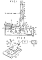
- an electron microscope has a tubular lens barrel 1 housing an electron gun 3 for emitting an electron beam 2 at a uniform speed, at least one convergent lens 4 comprising a magnetic lens or an electrostatic lens for converging the electron beam 2 toward a specimen 8, a specimen support 5, an objective lens 5 identical to the convergent lens 4, and a projector lens 7.
- the electron beam 2 having passed through the specimen 8 placed on the specimen support 5 is deflected by the objective lens 6 to form a magnified scattered-light image 8a of the specimen 8.
- the magnified scattered-light image 8a is focused by the projector lens 7 as an image 8b on an image-formation plane 9.
- An image recording device 10 is disposed below the tubular lens barrel 1.
- the image recording device 10 comprises a sensor supply unit 16 for storing a magazine 14 containing a number of stimulable phosphor sheets 12 serving as two-dimensional sensors, a recorder 18 including the image-formation plane 9, and a sensor receiving unit 22 for storing a magazine 20 identical to the magazine 14 in the sensor supply unit 16.
- An erase light source 24 is disposed between the sensor supply unit 16 and the recorder 18.
- a sheet supply table 26 is horizontally movably positioned between the sensor supply unit 16 and the recorder 18.
- the sheet supply table 26 has a rack 30 attached to the lower surface thereof and held in selective mesh with a plurality of pinions 28 spaced horizontally from each other.
- the sensor receiving unit 22 has a sheet delivery arm 32 for holding the stimulable phosphor sheet 12 in the recorder 18 and feeding the stimulable phosphor sheet 12 downwardly into the magazine 20.
- a shutter 34 and a fluorescent screen 36 which can be angularly movable in the direction of the arrow A by levers (not shown).
- the lens barrel 1 has an observation window 38 of lead glass formed in a wall thereof at a position above the shutter 34.
- the interiors of the lens barrel 1 and the image recording device 10 are kept under vacuum by a known vacuum pump while the electron microscope is in operation.
- the spaces in the lens barrel 1 and the image recording device 10 are isolated from each other by a shield (not shown) positioned between the lens barrel 1 and the image recording device 10. Therefore, the interior of the lens barrel 1 can be maintained under vacuum even when the interior of the image recording device 10 is vented to the atmosphere at the time of loading the magazine 14 or taking out the magazine 20.
- the sensor supply unit 16 is loaded with the magazine 14 containing a number of stimulable phosphor sheets 12 and the sensor receiving unit 22 is loaded with the magazine 20 which is empty.
- the shutter 34 and the fluorescent screen 36 are held in a horizontal position (as shown) to shield the recorder 18 from the electron beam 2.
- the pinions 28 are rotated clockwise to move the sheet supply table 25 to the right for supplying the lowermost stimulable phosphor sheet 12 from the magazine 14 to the recorder 18.
- the erase light source 24 is energized to erase any remanent radiation energy from the sheet 12 (as described later in more detail).
- the sheet supply table 26 is stopped when the sheet 12 reaches the image-formation plane 9.
- the electron beam 2 impinges on the fluorescent screen 36 to enable the same to emit fluorescent radiation in the form of the magnified scattered-light image 8a which can be observed through the observation window 38.
- the shutter 34 and the fluorescent screen 36 are lifted by the non-illustrated levers to the elevated position (indicated by the dotted lines).
- the electron beam 2 is now allowed to reach the stimulable phosphor sheet 12 set in the recorder 18.
- the electron beam energy which carries the magnified scattered-light image 8b is then stored in the sheet 12.
- the shutter 34 is closed.
- the stimulable phosphor sheet 12 on which the magnified scattered-light image 8a is recorded is then fed by the sheet delivery arm 32 into the magazine 20.
- the sheet supply table 26 is moved back from the recorder 18 to the sensor supply unit 16 for supplying another stimulable phosphor sheet 12 to the recorder 18 in the next recording cycle.
- FIG. 2 shows an image reader system for reading the recorded image from a stimulable phosphor sheet 12. As shown in Figure 2, the stimulable phosphor sheet 12 is positioned on a sheet transport means 40 comprising an endless belt, for example.
- a stimulating light beam 44 emitted from a stimulating light source 42 such as an He-Ne laser emission tube is deflected by a light deflector 46 such as a galvanometer mirror to scan the stimulable phosphor sheet 12 in the direction of the arrow X (primary scanning mode).
- the sheet transport means 40 is operated to move the stimulable phosphor sheet 12 in the direction of the arrow Y (secondary scanning mode) which is substantially perpendicular to the primary scanning direction. Therefore, the entire surface of the stimulable phosphor sheet 12 is exposed to the stimulating light beam 44.
- the stimulable phosphor sheet 12 Upon exposure to the stimulating light beam 44, the stimulable phosphor sheet 12 emits photofluorescent radiation 48 having a level dependent on the electron beam energy stored in the sheet 12.
- the emitted light 48 enters a light collector 50 through its entrance end 50a and goes through the light collector 50 while repeating total reflection therein.
- the light 48 is then discharged from the light collector 50 through its exit end 50b and detected by a light detector 52 such as a photomultiplier coupled to the exit end 50b.
- the photofluorescent light emitted from the stimulable phosphor sheet 12 is therefore photoelectrically read by the light detector 52.
- the electric signal produced by the light detector 52 is therefore representative of the level of the electron beam energy stored in the stimulable phosphor sheet 12.
- the electric signal from the light detector 52 is processed by an image processor 54, and then applied to an image reproducing unit 56 such as a display unit comprising a CRT.
- the image reproducing unit 56 may be a recording device for optically scanning a photosensitive film to record the image thereon. Therefore, the magnified scattered-light image 8b carried by the photofluorescent light 48 can be reproduced by the image reproducing unit 56.
- Figure 3 shows an example of an image scanner which can be used as the image reproducing unit 56.
- a photosensitive film 130 By moving a photosensitive film 130 in the sub-scanning direction of arrow Y and having a laser beam 131 scan the film 130 in the direction of the arrow X, and further by modulating the laser beam 131 by an A/D modulator 132 based on an image signal from the image processor 54, a visible image is formed on the photosensitive film 130.
- the size of the visible image formed on the photosensitive film 130 is made larger than the size of the image-formation plane 9 (i.e., corresponding to the area of image recording on the two-dimensional sensor) and the magnified scattered-light image 8b is reproduced in an enlarged scale. Since the magnified scattered-light image 8b is reproduced with high sharpness when a stimulable phosphor sheet 10 is used, it is possible to reproduce an enlarged image of sufficiently high image quality. Therefore, it is possible to use a stimulable phosphor sheet 10 of small size and also possible to use a photodetector of small size, whereby the apparatus can be made compact in size.
- the density of scanning lines is made higher in reproduction than that in read-out when the stored image is read out from the stimulable phosphor sheet.
- the density of scanning lines is preferably determined not lower than 10 pixels (picture elements)/mm, more preferably in the range of 15 pixels/mm to 100 pixels/mm, and when the image is reproduced the density of scanning lines is desired to be made lower, preferably in the range of 5 pixels/mm to 20 pixels/mm.
- the stimulable phosphor sheet 12 When the stimulable phosphor sheet 12 is exposed to the stimulating light, not all of the electron beam energy stored in the sheet 12 is discharged, a remanent electron microscope image tending to remain on the sheet 12. In addition, the stimulable phosphor sheet 12 is liable to contain noise arising from environmental radiation or radiation from radioactive elements such as Ra mixed as impurities in the phosphor. To remove such a remanent image or noise, the stimulable phosphor sheet 12 as it is carried by the sheet supply table 26 is exposed to erasing light 58 emitted from the erase light source 24 as shown in Figure 1, the erasing light 58 being of a wavelength falling within the wavelength range of the stimulating light to be applied to the stimulable phosphor sheet 12.
- the residual radiation energy is therefore erased from the sheet 12 by exposure to the erasing light 58.
- the erase light source 24 may comprise a tungsten lamp, halogen lamp, an infrared lamp, a xenon flash lamp, or a laser beam source, as shown in Japanese Unexamined Patent Publication No. 56(1981)-11392.
- the remanent image or noise can also be erased by heating the stimulable phosphor sheet 12.
- the stimulable phosphor sheet 12 from which the image has been read can be recycled by being stored in the magazine 14 which is loaded in the sensor supply unit 16.
- the stimulable phosphor sheet 12 with the recorded image read therefrom may be processed by a separate erasing device having a light source similar to the erase light source 24.
- the erase light source 24 in the image recording device 10 is employed primarily for erasing the small noise arising from the environmental radiation or radiation from radioactive elements such as radium (Ra) mixed as impurities in the phosphor, or a slight trace of the previously recorded image.
- the erase light source 24 can therefore be of a relatively small capacity.
- the amount of erasing light to be radiated onto the stimulable phosphor sheet 12 is shown in detail in Japanese Unexamined Patent Publication No. 58(1983)-80633, for example. Since the amount of erasing light to be emitted is equal to the product of illuminance and time, the desired amount of erasing light can be attained by varying the intensity of erasing light emitted from the erase light source 24 or the speed of travel of the stimulable phosphor sheet 12 below the erase light source 24.
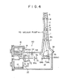
- FIG. 1 Figure illustrates an image recording device 60 according to another embodiment of the present invention.
- the sensor supply unit 16 and the sensor receiving anit 22 are vertically aligned.
- the stimulable phosphor sheets 12 in the magazine 14 loaded in the sensor supply unit 16 are removed one by one from the magazine 14 by a sheet feed arm 62 which grips the leading end of the sheet 12.
- the atimulable phosphor sheet 12 fed from the sensor supply unit 16 is then fed between two guide plates 64 and transported Ly sheet feed rollers 66 and sheet feed and discharge rollers f8a, 68b, 68c over a guide plate 70 to the recorder 18 which includes the image-formation plane 9.
- the sheet 12 While the stimulable phosphor sheet 12 is being delivered from the senscr supply unit 16 to the recorder 18, the sheet 12 is exposed to the erasing light 58 emitted by the erase light source 24 to erase the residual radiation energy from the sheet 12.
- the stimulable phosphor sheet 12 is held in the image-formation plane 9 by the sheet feed and discharge rollers 68b, 68c in the recorder 18.
- the magnified scattered-light image 8b of the specimen 8 is then recorded on the stimulable phosphor sheet 12.
- the sheet feed and discharge rollers 68b, 68c are reversed and the guide plate 70 is tilted to the dotted-line position to deliver the sheet 12 through the sheet feed rollers 68a and discharge rollers 72 and between two guide plates 74.
- the stimulable phosphor sheet 12 is then discharged into the magazine 20 in the sheet receiving unit 22 by a sheet discharge arm 76 which is identical to the sheet feed arm 62.
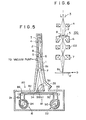
- FIG. 5 shows an image recording device 80 according to still another embodiment of the present invention.
- the image recording device 80 employs a belt-like stimulable phosphor sheet 82 serving as a two-dimensional sensor.
- the stimulable phosphor sheet 82 as it is wound around a sheet supply roll 84 is housed in the sensor supply unit 16.
- the stimulable phosphor sheet 82 is unwound from the sheet supply roll 84 and kept taut between sheet holder rollers 86, 88 so as to lie in the image-formation plane 9.
- the stimulable phosphor sheet 82 has its leading end engaging a sheet takeup roll 90 in the sensor receiving unit 22.
- the sheet takeup roll 90 is rotated to deliver the sheet 82 a prescribed length from the sheet supply roll 84 to the sheet takeup roll 90.
- magnified scattered-light images 8b are successively recorded on successive areas of the stimulable phosphor sheet 12.
- the stimulable phosphor sheet 12 as it is fed from the sheet supply roll 84 to the recorder 18 is exposed to the erasing light 58 from the erase light source 24 for thereby erasing undesired remanent radiation energy from the sheet 82.
- the stimulable phosphor sheet 82 When the stimulable phosphor sheet 82 is fully consumed and wound up by the sheet takeup roll 90, it is removed together with the sheet takeup roll 90 from the sensor receiving unit 22, or is wound back on the sheet supply roll 84 and removed together with the sheet supply roll 84 from the sheet supply unit 16.
- the stimulable phosphor sheet 82 is then processed by the image reader system in the manner described above.
- the stimulable phosphor sheet 12 in the sensor supply unit 16, the recorder 18, and the sensor receiving unit 22 is shielded from light by a shield 92.
- the erase light source 24 may be energized at all times. From the economical standpoint, however, the erase light source 24 should be energized only for required time periods.
- the erase light source 24 in each of the foregoing embodiments may be located outside of the image recording device, and the stimulable phosphor sheet may be exposed to erasing light transmitted from the erase light source 24 through a light-transmissive window in the wall of the image recording device.
- the image recording device of the present invention can be used for recording the diffraction pattern of a specimen.
- Figure 6 shows an electron microscope which can be employed in combination with the image recording device for recording such a diffraction pattern.
- the electron microscope generally denoted at 100, has an intermediate lens 102 disposed between the objective lens 6 and the projector lens 7.
- the diffraction pattern 8c of the specimen 8 which is formed on the rear focal plane of the objective lens 7, is magnified by the intermediate lens 102 and the projector lens 7 with their focal points on the rear focal plane of the objective lens 7 and is projected onto the image-formation plane 9.
- the magnified image of the diffraction pattern 8c can be recorded by the electron beam 2 on the stimulable phosphor sheet 12.
- the recorded diffraction pattern 8c can be reproduced by the image reader system shown in Figure 2, and the reproduced image can be displayed on the CRT or printed as a hard copy.
- the stimulable phosphor sheet may comprise a thermofluorescent phosphor sheet.
- the sheet may be scanned by thermal radiation emitted from a heat source such as a C0 2 laser source.
- a heat source such as a C0 2 laser source.
- the recorded electron microscope image is reproduced directly as an electric signal, which can be processed in various ways such as tone processing, frequency emphasis, etc.
- various image processing modes such as the processing of a diffraction pattern, the reconstruction of a three-dimensional image, and the digitization of an image can easily and quickly be effected.
- the two-dimensional sensor for recording electron microscope images can be reused through exposure to erasing light or heat, electron microscope images can be recorded more economically than would be with the conventional silver-salt photographic system.
- Many electron microscope images can successively be recorded on separate two-dimensional sensors or a single belt-like two-dimensional sensor in an automatic process by feeding the successive two-dimensional sensors or the single two-dimensional sensor from the sensor supply unit through the recorder into the sensor receiving unit.
- the recorded electron microscope images are of a good S/N ratio as undesired remanent images and noise are erased before the images are recorded.
Landscapes
- Physics & Mathematics (AREA)
- Health & Medical Sciences (AREA)
- Life Sciences & Earth Sciences (AREA)
- General Physics & Mathematics (AREA)
- High Energy & Nuclear Physics (AREA)
- Molecular Biology (AREA)
- Spectroscopy & Molecular Physics (AREA)
- Chemical & Material Sciences (AREA)
- Analytical Chemistry (AREA)
- Conversion Of X-Rays Into Visible Images (AREA)
Applications Claiming Priority (2)
| Application Number | Priority Date | Filing Date | Title |
|---|---|---|---|
| JP59214682A JPH0616395B2 (ja) | 1984-10-12 | 1984-10-12 | 電子顕微鏡像記録装置 |
| JP214682/84 | 1984-10-12 |
Publications (2)
| Publication Number | Publication Date |
|---|---|
| EP0181507A1 true EP0181507A1 (de) | 1986-05-21 |
| EP0181507B1 EP0181507B1 (de) | 1991-05-29 |
Family
ID=16659834
Family Applications (1)
| Application Number | Title | Priority Date | Filing Date |
|---|---|---|---|
| EP19850112937 Expired EP0181507B1 (de) | 1984-10-12 | 1985-10-11 | Vorrichtung zur Aufzeichnung eines Bildes mittels eines Elektronenmikroskops |
Country Status (3)
| Country | Link |
|---|---|
| EP (1) | EP0181507B1 (de) |
| JP (1) | JPH0616395B2 (de) |
| DE (1) | DE3583003D1 (de) |
Cited By (2)
| Publication number | Priority date | Publication date | Assignee | Title |
|---|---|---|---|---|
| EP0249214A3 (de) * | 1986-06-11 | 1991-01-02 | Manfred R. Kuehnle | System zur elektrophotographischen Bildaufzeichnung |
| US4988874A (en) * | 1988-09-14 | 1991-01-29 | Fuji Photo Film Co., Ltd. | Recording medium magazine for electron microscopes |
Families Citing this family (5)
| Publication number | Priority date | Publication date | Assignee | Title |
|---|---|---|---|---|
| JPS6358749A (ja) * | 1986-08-29 | 1988-03-14 | Jeol Ltd | 透過電子顕微鏡 |
| JPS63164152A (ja) * | 1986-12-25 | 1988-07-07 | Fuji Photo Film Co Ltd | 電子顕微鏡像記録再生方法 |
| JPS63174253A (ja) * | 1987-01-13 | 1988-07-18 | Fuji Photo Film Co Ltd | 電子顕微鏡 |
| JPH01100859A (ja) * | 1987-10-09 | 1989-04-19 | Fuji Photo Film Co Ltd | 電子顕微鏡 |
| JPH01117259A (ja) * | 1987-10-30 | 1989-05-10 | Fuji Photo Film Co Ltd | 電子顕微鏡 |
Citations (2)
| Publication number | Priority date | Publication date | Assignee | Title |
|---|---|---|---|---|
| US3823322A (en) * | 1971-11-30 | 1974-07-09 | Siemens Ag | Photographic film handling apparatus for charged-particle beam equipment |
| EP0077676B1 (de) * | 1981-10-16 | 1986-08-06 | Fuji Photo Film Co., Ltd. | Strahlungsbild-Aufzeichnungssystem |
Family Cites Families (3)
| Publication number | Priority date | Publication date | Assignee | Title |
|---|---|---|---|---|
| JPS4831684A (de) * | 1971-08-25 | 1973-04-25 | ||
| JPS57119340A (en) * | 1981-01-16 | 1982-07-24 | Fuji Photo Film Co Ltd | Radiation picture recorder |
| JPS58122500A (ja) * | 1982-01-14 | 1983-07-21 | 富士写真フイルム株式会社 | 放射線像変換パネル |
-
1984
- 1984-10-12 JP JP59214682A patent/JPH0616395B2/ja not_active Expired - Fee Related
-
1985
- 1985-10-11 EP EP19850112937 patent/EP0181507B1/de not_active Expired
- 1985-10-11 DE DE8585112937T patent/DE3583003D1/de not_active Expired - Lifetime
Patent Citations (2)
| Publication number | Priority date | Publication date | Assignee | Title |
|---|---|---|---|---|
| US3823322A (en) * | 1971-11-30 | 1974-07-09 | Siemens Ag | Photographic film handling apparatus for charged-particle beam equipment |
| EP0077676B1 (de) * | 1981-10-16 | 1986-08-06 | Fuji Photo Film Co., Ltd. | Strahlungsbild-Aufzeichnungssystem |
Cited By (2)
| Publication number | Priority date | Publication date | Assignee | Title |
|---|---|---|---|---|
| EP0249214A3 (de) * | 1986-06-11 | 1991-01-02 | Manfred R. Kuehnle | System zur elektrophotographischen Bildaufzeichnung |
| US4988874A (en) * | 1988-09-14 | 1991-01-29 | Fuji Photo Film Co., Ltd. | Recording medium magazine for electron microscopes |
Also Published As
| Publication number | Publication date |
|---|---|
| JPS6193541A (ja) | 1986-05-12 |
| JPH0616395B2 (ja) | 1994-03-02 |
| DE3583003D1 (de) | 1991-07-04 |
| EP0181507B1 (de) | 1991-05-29 |
Similar Documents
| Publication | Publication Date | Title |
|---|---|---|
| EP0177973B1 (de) | Aufnahme- und Wiedergabeverfahren von erzeugten Bildern mittels eines Elektronenmikroskops | |
| US4889990A (en) | Method and apparatus for recording and reproducing electron microscope image | |
| EP0181446B1 (de) | Strahlungsbildaufnahme- und Wiedergabesystem | |
| US4507797A (en) | Data recording system using stimulable phosphor | |
| EP0184810A2 (de) | Verfahren zur Feststellung eines Fokussierungsfehlers eines elektronen-mikroskopischen Bildes | |
| EP0181507B1 (de) | Vorrichtung zur Aufzeichnung eines Bildes mittels eines Elektronenmikroskops | |
| EP0183262B1 (de) | Verfahren zur Aufzeichnung und Wiedergabe von durch ein Elektronenmikroskop erzeugten Bildern | |
| US4584483A (en) | Noise erasing method in radiation image recording and reproducing method | |
| US4851677A (en) | Apparatus for recording and reproducing image produced by an electron microscope including an optical filter and a deflecting element | |
| EP0178672B1 (de) | Elektronenmikroskop | |
| US4801801A (en) | Transmission-type electron microscope | |
| US4700071A (en) | Method of recording and reproducing an electron microscope image | |
| US4847497A (en) | Apparatus for recording images produced by an electron microscope | |
| US5006707A (en) | Electron microscope image recording and read-out method | |
| JPH0616394B2 (ja) | 電子顕微鏡像記録再生方法 | |
| JPH0616397B2 (ja) | 電子顕微鏡像記録読取装置 | |
| JPH0616393B2 (ja) | 電子顕微鏡像記録再生方法 | |
| JPH04319938A (ja) | 放射線像変換システムの検査方法、それに用いられる消去露光装置および放射線像読取装置 | |
| JPH06231714A (ja) | 蓄積性蛍光体シートホルダおよびそれを使用した電子顕微鏡像記録読取方法および装置 | |
| JPH0616396B2 (ja) | 電子顕微鏡像記録再生方法 | |
| JPH0616398B2 (ja) | 電子顕微鏡のデフオ−カス量測定方法 | |
| JPS61138442A (ja) | 電子顕微鏡像記録再生方法 | |
| JPS62145635A (ja) | 透過型電子顕微鏡 | |
| JPH06223764A (ja) | 電子顕微鏡像記録読取方法および装置 | |
| JPH04320248A (ja) | カラー画像情報記録読取方法および装置 |
Legal Events
| Date | Code | Title | Description |
|---|---|---|---|
| PUAI | Public reference made under article 153(3) epc to a published international application that has entered the european phase |
Free format text: ORIGINAL CODE: 0009012 |
|
| AK | Designated contracting states |
Kind code of ref document: A1 Designated state(s): DE FR NL |
|
| 17P | Request for examination filed |
Effective date: 19860619 |
|
| 17Q | First examination report despatched |
Effective date: 19880129 |
|
| GRAA | (expected) grant |
Free format text: ORIGINAL CODE: 0009210 |
|
| AK | Designated contracting states |
Kind code of ref document: B1 Designated state(s): DE FR NL |
|
| ET | Fr: translation filed | ||
| REF | Corresponds to: |
Ref document number: 3583003 Country of ref document: DE Date of ref document: 19910704 |
|
| PLBE | No opposition filed within time limit |
Free format text: ORIGINAL CODE: 0009261 |
|
| STAA | Information on the status of an ep patent application or granted ep patent |
Free format text: STATUS: NO OPPOSITION FILED WITHIN TIME LIMIT |
|
| 26N | No opposition filed | ||
| PGFP | Annual fee paid to national office [announced via postgrant information from national office to epo] |
Ref country code: NL Payment date: 20021017 Year of fee payment: 18 Ref country code: FR Payment date: 20021017 Year of fee payment: 18 |
|
| PGFP | Annual fee paid to national office [announced via postgrant information from national office to epo] |
Ref country code: DE Payment date: 20021127 Year of fee payment: 18 |
|
| PG25 | Lapsed in a contracting state [announced via postgrant information from national office to epo] |
Ref country code: NL Free format text: LAPSE BECAUSE OF NON-PAYMENT OF DUE FEES Effective date: 20040501 Ref country code: DE Free format text: LAPSE BECAUSE OF NON-PAYMENT OF DUE FEES Effective date: 20040501 |
|
| PG25 | Lapsed in a contracting state [announced via postgrant information from national office to epo] |
Ref country code: FR Free format text: LAPSE BECAUSE OF NON-PAYMENT OF DUE FEES Effective date: 20040630 |
|
| NLV4 | Nl: lapsed or anulled due to non-payment of the annual fee |
Effective date: 20040501 |
|
| REG | Reference to a national code |
Ref country code: FR Ref legal event code: ST |