EP0182571A2 - Dispositif de commutation à semi-conducteurs - Google Patents
Dispositif de commutation à semi-conducteurs Download PDFInfo
- Publication number
- EP0182571A2 EP0182571A2 EP85308189A EP85308189A EP0182571A2 EP 0182571 A2 EP0182571 A2 EP 0182571A2 EP 85308189 A EP85308189 A EP 85308189A EP 85308189 A EP85308189 A EP 85308189A EP 0182571 A2 EP0182571 A2 EP 0182571A2
- Authority
- EP
- European Patent Office
- Prior art keywords
- transistor
- base
- voltage
- bipolar transistor
- current
- Prior art date
- Legal status (The legal status is an assumption and is not a legal conclusion. Google has not performed a legal analysis and makes no representation as to the accuracy of the status listed.)
- Ceased
Links
Images
Classifications
-
- H—ELECTRICITY
- H03—ELECTRONIC CIRCUITRY
- H03K—PULSE TECHNIQUE
- H03K17/00—Electronic switching or gating, i.e. not by contact-making and –breaking
- H03K17/51—Electronic switching or gating, i.e. not by contact-making and –breaking characterised by the components used
- H03K17/56—Electronic switching or gating, i.e. not by contact-making and –breaking characterised by the components used by the use, as active elements, of semiconductor devices
- H03K17/567—Circuits characterised by the use of more than one type of semiconductor device, e.g. BIMOS, composite devices such as IGBT
Definitions
- This invention relates to a semiconductor switching device.
- Compound transistor pairs consisting of a bipolar transistor and a field effect transistor in a cascade arrangement are well known. They seek to combine the speed of a field effect transistor with the voltage handling capacity of a bipolar transistor. It has also been known to connect a zener diode as a voltage reference device between the base of the bipolar transistor and the source of the field effect transistor for improving the switching properties of the transistor pair.
- a semiconductor device comprising a compound transistor pair including a bipolar transistor and a field effect transistor connected to form a series circuit of the emitter and collector of the bipolar transistor and the source and drain of the bipolar transistor, an auxiliary switch having a pair of main current-handling terminals and a control terminal, one of the pair of current-handling terminals being connected to the source of the field effect transistor and the other to the base of the bipolar transistor, and voltage threshold switching means connected between the base of the bipolar transistor and the control terminal of the auxiliary switch so that while the compound transistor pair is conductive the voltage threshold switching means blocks current supply from the base of the bipolar transistor to the control terminal of the auxiliary switch and when the compound transistor pair is switched off the resultant rise in voltage across the voltage threshold switching means causes the latter to supply current from the base of the bipolar transistor to the control terminal of the auxiliary switch so that the latter becomes conductive between the base of the bipolar transistor and said source of the field effect transistor.
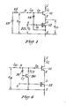
- FIG. 1 there is shown a prior art switching circuit.
- a compound transistor pair comprises a bipolar transistor 11, shown as an NPN-type, and an FET 12, shown as an N-channel type.
- the circuit is powered by voltage supply 13 connected between the base B of transistor 11 and the source S of transistor 12.
- Switching voltage e G is applied to the gate G of transistor 12 and a load (not shown) is connected in series with transistors 11 and 12 to receive collector current I C' Zener diode 14 is connected between the base of transistor 11 and the source of transistor 12.
- the zener diode is poled to have its cathode terminal connected to the base of transistor 11.
- a current-limiting resistor 15 is also included.
- Such a circuit is designed so that its switching speed is largely determined by the relatively fast switching speed of the FET and its ability to handle high operating voltages is largely provided by the ability of the bipolar transistor to withstand high operating voltages supplied by the source 13.
- a switching voltage is applied to the gate of the transistor 12, quickly turning it on whereby the voltage drop V DS across the drain and source of the transistor 12 falls sharply, allowing the voltage provided by supply 13 to be applied largely to the base of the transistor 11 for providing a forward bias to its emitter whereby a large base current is supplied and the transistor 11 and in turn the compound pair can be turned on sharply.
- turn-off voltage is applied to the gate of the transistor 12, to turn it off.
- the current I C which had been flowing through the base-emitter junction of transistor 11 is temporarily shifted into the zener diode 14 whereby storage of carriers in the base of the transistor 11 is avoided and the transistor 11 and in turn the compound pair can be turned off rapidly whereby the collector current I - also can be turned off rapidly.
- One role of the zener diode 14 is, as a voltage reference device, to maintain the voltage drop V DS below its blocking voltage BV DS , at which voltage it can turn off, at the time of switching the collector current I C .
- the other role is to serve as a high resistance path while the compound pair is conducting to divert as little as possible of the current being supplied by the source 13.
- the voltage BV DS is represented by the following equation where V ZL is the voltage across the diode when a load current equal to I C flows through it and V BE10 is the forward voltage drop across the base-emitter path of the bipolar transistor immediately before the collector current passing through the base and emitter junction ceases.
- the last equation indicates that for a low BV DS , a diode of low V ZO and low resistance is desired.
- the ordinary zener diode with a low V ZO tends to have a high R Z .
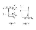
- a circuit (as shown in Fig. 2) employing a series of ordinary forward-biased diodes connected in the forward direction can be employed as the equivalent of a zener diode to achieve a better combination of low V ZO and low R Z .
- such an arrangement tends to have a very soft breakdown characteristic and the unloaded zener voltage V ZO is considerably lower than the voltage drop when a current I C flows through the diode arrangement.
- the voltage V ZO must satisfy the following condition where V BE(Sat) is the base-emitter forward voltage drop of the transistor 11 when the transistor is on, and V DSON is the voltage drop across the FET 12 when it is on.
- Figs. 4 and 5 are designed to avoid this dilemma. They permit use of a zener diode with as low a V ZO as possible, consistent with its satisfying the condition of equation (3) above. It is characteristic of these circuits that ideally they provide characteristics which are essentially those of an ideal zener diode with the unloaded zener voltage V ZO being substantially the same as the loaded zener voltage V ZL '
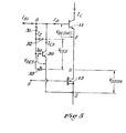
- Fig. 4 there is shown a first embodiment of the invention. Elements corresponding to elements in the prior art circuit shown in Fig. 1 have been given the same reference numerals.
- the distinctive feature over the prior art circuit is the inclusion of a circuit branch made up of auxiliary transistor 30, shown here as a bipolar NPN transistor, and a zener diode 31.
- the collector of transistor 30 is connected to the base of transistor 11 and the emitter to the source of transistor 12.
- the cathode of zener diode 31 is connected to the base of transistor 11 and the anode to the base of the transistor 30.
- the current I C is switched into the equivalent zener diode circuit branch.
- the voltage across diode 31 rises and when it exceeds V ZO , zener current starts to flow, which in turn provides base current to the auxiliary transistor 30 which then conducts.
- the zener current I Z remains less than the current I C and, accordingly, the voltage across the zener diode and in turn the base voltage of the transistor 11 is held at a value near to the unloaded zener voltage V ZO of the diode 31. Accordingly, by treating the base voltage at this time as the loaded zener voltage of the ideal zener diode, the condition of equation 1 is satisfied.
- the preferred embodiment shown in Fig. 5 is directed to solving this problem.
- This embodiment differs from the previous embodiment by the inclusion of a high valued resistor 32 between the base and collector of the transistor 30 and a high-valued variable resistor 33 between the base and emitter of the transistor 30 to form a voltage-divider.
- the auxiliary transistor 30 when the collector current I C is at the desired limit value, the auxiliary transistor 30 is maintained at the point just before it starts to let flow its collector current I C3 , by means of resistors 32 and 33.
- resistor 32 is of fixed high value and resistor 33 of high adjustable value, and adjusting it to achieve the desired result.
- resistors 32 and 33 are chosen such that when the compound transistor pair is ON, essentially all the current that flows from source 13 flows into the base of transistor 11.
- the collector-emitter voltage of transistor 30 rises more rapidly and to a higher level than in the case where the pair is in the ON state, and the zener diode 31 comes into conduction and the zener current joins the base current of transistor 30. Accordingly, while the collector-emitter voltage of transistor 30 is maintained substantially constant as described previously, most of the current I C diverted from the pair changes into collector current of transistor 30 whereby a high speed turning-off is achieved.
- each provide a semiconductor device comprising a compound transistor pair including a bipolar transistor 11 and a field effect transistor 12 connected to form a series circuit of the emitter E and collector C of the bipolar transistor and the source S and drain D of the bipolar transistor, an auxiliary switch 30 having a pair of main current-handling terminals and a control terminal, one of the pair of current-handling terminals being connected to the source S of the field effect transistor 12 and the other to the base B of the bipolar transistor 11, and voltage threshold switching means 31 connected between the base B of the bipolar transistor 11 and the control terminal of the auxiliary switch 30 so that while the compound transistor pair is conductive the voltage threshold switching means 31 blocks current supply from the base B of the bipolar transistor 11 to the control terminal of the auxiliary switch 30 and when the compound transistor pair is switched off the resultant rise in voltage across the voltage threshold switching means 31 causes the latter to supply current from the base B of the bipolar transistor 11 to the control terminal of the auxiliary switch 30 so that the latter becomes conductive between the base B of the bipolar transistor
- auxiliary transistor described above comprises a bipolar transistor, it may be replaced by any suitable auxiliary switch such as a field effect transistor.
- the zener diode 31 may be replaced by any suitable voltage threshold switching means.
- invention should be useful with other forms of voltage reference devices which have soft breakdown characteristics.
Landscapes
- Electronic Switches (AREA)
Applications Claiming Priority (4)
| Application Number | Priority Date | Filing Date | Title |
|---|---|---|---|
| JP59238899A JPS61117919A (ja) | 1984-11-13 | 1984-11-13 | 半導体装置 |
| JP238899/84 | 1984-11-13 | ||
| JP238900/84 | 1984-11-13 | ||
| JP59238900A JPS61117920A (ja) | 1984-11-13 | 1984-11-13 | 半導体装置 |
Publications (2)
| Publication Number | Publication Date |
|---|---|
| EP0182571A2 true EP0182571A2 (fr) | 1986-05-28 |
| EP0182571A3 EP0182571A3 (fr) | 1988-09-14 |
Family
ID=26533968
Family Applications (1)
| Application Number | Title | Priority Date | Filing Date |
|---|---|---|---|
| EP85308189A Ceased EP0182571A3 (fr) | 1984-11-13 | 1985-11-11 | Dispositif de commutation à semi-conducteurs |
Country Status (2)
| Country | Link |
|---|---|
| US (1) | US4651035A (fr) |
| EP (1) | EP0182571A3 (fr) |
Cited By (1)
| Publication number | Priority date | Publication date | Assignee | Title |
|---|---|---|---|---|
| DE3717122A1 (de) * | 1986-09-26 | 1988-03-31 | Mitsubishi Electric Corp | Treiber-schaltung |
Families Citing this family (5)
| Publication number | Priority date | Publication date | Assignee | Title |
|---|---|---|---|---|
| DE3586735D1 (de) * | 1984-10-19 | 1992-11-12 | Bbc Brown Boveri & Cie | Abschaltbares leistungshalbleiterbauelement. |
| CH668667A5 (de) * | 1985-11-15 | 1989-01-13 | Bbc Brown Boveri & Cie | Leistungshalbleitermodul. |
| JPH01133414A (ja) * | 1987-11-18 | 1989-05-25 | Mitsubishi Electric Corp | カスコードBiMOS駆動回路 |
| EP0380799B1 (fr) * | 1989-02-02 | 1993-10-06 | Asea Brown Boveri Ag | Composant semi-conducteur à contact de pression |
| US5006736A (en) * | 1989-06-13 | 1991-04-09 | Motorola, Inc. | Control circuit for rapid gate discharge |
Family Cites Families (5)
| Publication number | Priority date | Publication date | Assignee | Title |
|---|---|---|---|---|
| US3610960A (en) * | 1968-05-21 | 1971-10-05 | Rca Corp | Scan generator circuit |
| GB2053606B (en) * | 1979-06-01 | 1983-09-14 | Gould Advance Ltd | Semi-conductor switching circuits |
| US4425516A (en) * | 1981-05-01 | 1984-01-10 | Zytrex Corporation | Buffer circuit and integrated semiconductor circuit structure formed of bipolar and CMOS transistor elements |
| US4487457A (en) * | 1982-09-28 | 1984-12-11 | Eaton Corporation | Gating circuit for combining series and parallel connected FETs |
| DE3240778A1 (de) * | 1982-11-04 | 1984-05-10 | Siemens AG, 1000 Berlin und 8000 München | Elektronischer schalter |
-
1985
- 1985-10-09 US US06/785,878 patent/US4651035A/en not_active Expired - Fee Related
- 1985-11-11 EP EP85308189A patent/EP0182571A3/fr not_active Ceased
Cited By (1)
| Publication number | Priority date | Publication date | Assignee | Title |
|---|---|---|---|---|
| DE3717122A1 (de) * | 1986-09-26 | 1988-03-31 | Mitsubishi Electric Corp | Treiber-schaltung |
Also Published As
| Publication number | Publication date |
|---|---|
| US4651035A (en) | 1987-03-17 |
| EP0182571A3 (fr) | 1988-09-14 |
Similar Documents
| Publication | Publication Date | Title |
|---|---|---|
| US4367421A (en) | Biasing methods and circuits for series connected transistor switches | |
| US4492883A (en) | Unpowered fast gate turn-off FET | |
| US4360744A (en) | Semiconductor switching circuits | |
| US4429339A (en) | AC Transistor switch with overcurrent protection | |
| US20050128669A1 (en) | Protection device | |
| EP0110355A2 (fr) | Circuit de régulation de la puissance de sortie pour amplificateur de puissance | |
| JPS59100621A (ja) | 電子スイツチ | |
| US4841166A (en) | Limiting shoot-through current in a power MOSFET half-bridge during intrinsic diode recovery | |
| EP0437108A2 (fr) | Circuit de commande pour commuter du courant dans une charge | |
| US4672245A (en) | High frequency diverse semiconductor switch | |
| US4740722A (en) | Composite semiconductor device | |
| US5475329A (en) | Turn-off circuit to provide a discharge path from a first node to a second node | |
| KR19980064368A (ko) | 하이 사이드 mosfet 게이트 보호 분류기 회로 | |
| US4125787A (en) | Semiconductor switch circuit | |
| EP0182571A2 (fr) | Dispositif de commutation à semi-conducteurs | |
| US4117351A (en) | Transistor switching circuit | |
| US3050636A (en) | High speed transistor switch | |
| US4777386A (en) | Driver circuit for a bipolar Darlington power transistor | |
| US4376900A (en) | High speed, non-saturating, bipolar transistor logic circuit | |
| US4400635A (en) | Wide temperature range switching circuit | |
| EP0219925A1 (fr) | Dispositif de commutation | |
| US4112315A (en) | Semiconductor switch circuit | |
| US6635930B1 (en) | Protective circuit | |
| US5430401A (en) | Electronic switches | |
| GB2053606A (en) | Improvements in and relating to semiconductor switching circuits |
Legal Events
| Date | Code | Title | Description |
|---|---|---|---|
| PUAI | Public reference made under article 153(3) epc to a published international application that has entered the european phase |
Free format text: ORIGINAL CODE: 0009012 |
|
| AK | Designated contracting states |
Kind code of ref document: A2 Designated state(s): DE FR GB |
|
| 17P | Request for examination filed |
Effective date: 19860715 |
|
| PUAL | Search report despatched |
Free format text: ORIGINAL CODE: 0009013 |
|
| AK | Designated contracting states |
Kind code of ref document: A3 Designated state(s): DE FR GB |
|
| 17Q | First examination report despatched |
Effective date: 19890913 |
|
| STAA | Information on the status of an ep patent application or granted ep patent |
Free format text: STATUS: THE APPLICATION HAS BEEN REFUSED |
|
| 18R | Application refused |
Effective date: 19900430 |
|
| RIN1 | Information on inventor provided before grant (corrected) |
Inventor name: HISAO, SHIGEKANE |