EP0183146A2 - Halbleiteranordnung mit epitaxialem Material - Google Patents
Halbleiteranordnung mit epitaxialem Material Download PDFInfo
- Publication number
- EP0183146A2 EP0183146A2 EP85114551A EP85114551A EP0183146A2 EP 0183146 A2 EP0183146 A2 EP 0183146A2 EP 85114551 A EP85114551 A EP 85114551A EP 85114551 A EP85114551 A EP 85114551A EP 0183146 A2 EP0183146 A2 EP 0183146A2
- Authority
- EP
- European Patent Office
- Prior art keywords
- layer
- dirac
- layers
- monoatomic
- semiconductor device
- Prior art date
- Legal status (The legal status is an assumption and is not a legal conclusion. Google has not performed a legal analysis and makes no representation as to the accuracy of the status listed.)
- Granted
Links
Images




Classifications
-
- H—ELECTRICITY
- H10—SEMICONDUCTOR DEVICES; ELECTRIC SOLID-STATE DEVICES NOT OTHERWISE PROVIDED FOR
- H10H—INORGANIC LIGHT-EMITTING SEMICONDUCTOR DEVICES HAVING POTENTIAL BARRIERS
- H10H20/00—Individual inorganic light-emitting semiconductor devices having potential barriers, e.g. light-emitting diodes [LED]
- H10H20/80—Constructional details
- H10H20/81—Bodies
- H10H20/811—Bodies having quantum effect structures or superlattices, e.g. tunnel junctions
- H10H20/812—Bodies having quantum effect structures or superlattices, e.g. tunnel junctions within the light-emitting regions, e.g. having quantum confinement structures
-
- B—PERFORMING OPERATIONS; TRANSPORTING
- B82—NANOTECHNOLOGY
- B82Y—SPECIFIC USES OR APPLICATIONS OF NANOSTRUCTURES; MEASUREMENT OR ANALYSIS OF NANOSTRUCTURES; MANUFACTURE OR TREATMENT OF NANOSTRUCTURES
- B82Y20/00—Nanooptics, e.g. quantum optics or photonic crystals
-
- H—ELECTRICITY
- H01—ELECTRIC ELEMENTS
- H01S—DEVICES USING THE PROCESS OF LIGHT AMPLIFICATION BY STIMULATED EMISSION OF RADIATION [LASER] TO AMPLIFY OR GENERATE LIGHT; DEVICES USING STIMULATED EMISSION OF ELECTROMAGNETIC RADIATION IN WAVE RANGES OTHER THAN OPTICAL
- H01S5/00—Semiconductor lasers
- H01S5/30—Structure or shape of the active region; Materials used for the active region
- H01S5/305—Structure or shape of the active region; Materials used for the active region characterised by the doping materials used in the laser structure
-
- H—ELECTRICITY
- H01—ELECTRIC ELEMENTS
- H01S—DEVICES USING THE PROCESS OF LIGHT AMPLIFICATION BY STIMULATED EMISSION OF RADIATION [LASER] TO AMPLIFY OR GENERATE LIGHT; DEVICES USING STIMULATED EMISSION OF ELECTROMAGNETIC RADIATION IN WAVE RANGES OTHER THAN OPTICAL
- H01S5/00—Semiconductor lasers
- H01S5/30—Structure or shape of the active region; Materials used for the active region
- H01S5/34—Structure or shape of the active region; Materials used for the active region comprising quantum well or superlattice structures, e.g. single quantum well [SQW] lasers, multiple quantum well [MQW] lasers or graded index separate confinement heterostructure [GRINSCH] lasers
-
- H—ELECTRICITY
- H10—SEMICONDUCTOR DEVICES; ELECTRIC SOLID-STATE DEVICES NOT OTHERWISE PROVIDED FOR
- H10D—INORGANIC ELECTRIC SEMICONDUCTOR DEVICES
- H10D10/00—Bipolar junction transistors [BJT]
-
- H—ELECTRICITY
- H10—SEMICONDUCTOR DEVICES; ELECTRIC SOLID-STATE DEVICES NOT OTHERWISE PROVIDED FOR
- H10D—INORGANIC ELECTRIC SEMICONDUCTOR DEVICES
- H10D30/00—Field-effect transistors [FET]
- H10D30/40—FETs having zero-dimensional [0D], one-dimensional [1D] or two-dimensional [2D] charge carrier gas channels
- H10D30/47—FETs having zero-dimensional [0D], one-dimensional [1D] or two-dimensional [2D] charge carrier gas channels having two-dimensional [2D] charge carrier gas channels, e.g. nanoribbon FETs or high electron mobility transistors [HEMT]
- H10D30/471—High electron mobility transistors [HEMT] or high hole mobility transistors [HHMT]
- H10D30/475—High electron mobility transistors [HEMT] or high hole mobility transistors [HHMT] having wider bandgap layer formed on top of lower bandgap active layer, e.g. undoped barrier HEMTs such as i-AlGaN/GaN HEMTs
- H10D30/4755—High electron mobility transistors [HEMT] or high hole mobility transistors [HHMT] having wider bandgap layer formed on top of lower bandgap active layer, e.g. undoped barrier HEMTs such as i-AlGaN/GaN HEMTs having wide bandgap charge-carrier supplying layers, e.g. modulation doped HEMTs such as n-AlGaAs/GaAs HEMTs
-
- H—ELECTRICITY
- H10—SEMICONDUCTOR DEVICES; ELECTRIC SOLID-STATE DEVICES NOT OTHERWISE PROVIDED FOR
- H10D—INORGANIC ELECTRIC SEMICONDUCTOR DEVICES
- H10D62/00—Semiconductor bodies, or regions thereof, of devices having potential barriers
- H10D62/10—Shapes, relative sizes or dispositions of the regions of the semiconductor bodies; Shapes of the semiconductor bodies
- H10D62/17—Semiconductor regions connected to electrodes not carrying current to be rectified, amplified or switched, e.g. channel regions
- H10D62/213—Channel regions of field-effect devices
- H10D62/221—Channel regions of field-effect devices of FETs
- H10D62/228—Channel regions of field-effect devices of FETs having delta-doped channels
-
- H—ELECTRICITY
- H10—SEMICONDUCTOR DEVICES; ELECTRIC SOLID-STATE DEVICES NOT OTHERWISE PROVIDED FOR
- H10D—INORGANIC ELECTRIC SEMICONDUCTOR DEVICES
- H10D62/00—Semiconductor bodies, or regions thereof, of devices having potential barriers
- H10D62/60—Impurity distributions or concentrations
- H10D62/605—Planar doped, e.g. atomic-plane doped or delta-doped
-
- H—ELECTRICITY
- H10—SEMICONDUCTOR DEVICES; ELECTRIC SOLID-STATE DEVICES NOT OTHERWISE PROVIDED FOR
- H10D—INORGANIC ELECTRIC SEMICONDUCTOR DEVICES
- H10D62/00—Semiconductor bodies, or regions thereof, of devices having potential barriers
- H10D62/80—Semiconductor bodies, or regions thereof, of devices having potential barriers characterised by the materials
- H10D62/81—Semiconductor bodies, or regions thereof, of devices having potential barriers characterised by the materials of structures exhibiting quantum-confinement effects, e.g. single quantum wells; of structures having periodic or quasi-periodic potential variation
- H10D62/815—Semiconductor bodies, or regions thereof, of devices having potential barriers characterised by the materials of structures exhibiting quantum-confinement effects, e.g. single quantum wells; of structures having periodic or quasi-periodic potential variation of structures having periodic or quasi-periodic potential variation, e.g. superlattices or multiple quantum wells [MQW]
- H10D62/8161—Semiconductor bodies, or regions thereof, of devices having potential barriers characterised by the materials of structures exhibiting quantum-confinement effects, e.g. single quantum wells; of structures having periodic or quasi-periodic potential variation of structures having periodic or quasi-periodic potential variation, e.g. superlattices or multiple quantum wells [MQW] potential variation due to variations in composition or crystallinity, e.g. heterojunction superlattices
- H10D62/8162—Semiconductor bodies, or regions thereof, of devices having potential barriers characterised by the materials of structures exhibiting quantum-confinement effects, e.g. single quantum wells; of structures having periodic or quasi-periodic potential variation of structures having periodic or quasi-periodic potential variation, e.g. superlattices or multiple quantum wells [MQW] potential variation due to variations in composition or crystallinity, e.g. heterojunction superlattices having quantum effects only in the vertical direction, i.e. layered structures having quantum effects solely resulting from vertical potential variation
- H10D62/8164—Semiconductor bodies, or regions thereof, of devices having potential barriers characterised by the materials of structures exhibiting quantum-confinement effects, e.g. single quantum wells; of structures having periodic or quasi-periodic potential variation of structures having periodic or quasi-periodic potential variation, e.g. superlattices or multiple quantum wells [MQW] potential variation due to variations in composition or crystallinity, e.g. heterojunction superlattices having quantum effects only in the vertical direction, i.e. layered structures having quantum effects solely resulting from vertical potential variation comprising only semiconductor materials
-
- H—ELECTRICITY
- H10—SEMICONDUCTOR DEVICES; ELECTRIC SOLID-STATE DEVICES NOT OTHERWISE PROVIDED FOR
- H10D—INORGANIC ELECTRIC SEMICONDUCTOR DEVICES
- H10D62/00—Semiconductor bodies, or regions thereof, of devices having potential barriers
- H10D62/80—Semiconductor bodies, or regions thereof, of devices having potential barriers characterised by the materials
- H10D62/81—Semiconductor bodies, or regions thereof, of devices having potential barriers characterised by the materials of structures exhibiting quantum-confinement effects, e.g. single quantum wells; of structures having periodic or quasi-periodic potential variation
- H10D62/815—Semiconductor bodies, or regions thereof, of devices having potential barriers characterised by the materials of structures exhibiting quantum-confinement effects, e.g. single quantum wells; of structures having periodic or quasi-periodic potential variation of structures having periodic or quasi-periodic potential variation, e.g. superlattices or multiple quantum wells [MQW]
- H10D62/8171—Doping structures, e.g. doping superlattices or nipi superlattices
-
- H—ELECTRICITY
- H10—SEMICONDUCTOR DEVICES; ELECTRIC SOLID-STATE DEVICES NOT OTHERWISE PROVIDED FOR
- H10D—INORGANIC ELECTRIC SEMICONDUCTOR DEVICES
- H10D8/00—Diodes
- H10D8/40—Transit-time diodes, e.g. IMPATT or TRAPATT diodes
-
- H—ELECTRICITY
- H10—SEMICONDUCTOR DEVICES; ELECTRIC SOLID-STATE DEVICES NOT OTHERWISE PROVIDED FOR
- H10F—INORGANIC SEMICONDUCTOR DEVICES SENSITIVE TO INFRARED RADIATION, LIGHT, ELECTROMAGNETIC RADIATION OF SHORTER WAVELENGTH OR CORPUSCULAR RADIATION
- H10F30/00—Individual radiation-sensitive semiconductor devices in which radiation controls the flow of current through the devices, e.g. photodetectors
- H10F30/20—Individual radiation-sensitive semiconductor devices in which radiation controls the flow of current through the devices, e.g. photodetectors the devices having potential barriers, e.g. phototransistors
- H10F30/21—Individual radiation-sensitive semiconductor devices in which radiation controls the flow of current through the devices, e.g. photodetectors the devices having potential barriers, e.g. phototransistors the devices being sensitive to infrared, visible or ultraviolet radiation
-
- H—ELECTRICITY
- H10—SEMICONDUCTOR DEVICES; ELECTRIC SOLID-STATE DEVICES NOT OTHERWISE PROVIDED FOR
- H10F—INORGANIC SEMICONDUCTOR DEVICES SENSITIVE TO INFRARED RADIATION, LIGHT, ELECTROMAGNETIC RADIATION OF SHORTER WAVELENGTH OR CORPUSCULAR RADIATION
- H10F77/00—Constructional details of devices covered by this subclass
- H10F77/10—Semiconductor bodies
- H10F77/14—Shape of semiconductor bodies; Shapes, relative sizes or dispositions of semiconductor regions within semiconductor bodies
- H10F77/146—Superlattices; Multiple quantum well structures
-
- H—ELECTRICITY
- H01—ELECTRIC ELEMENTS
- H01S—DEVICES USING THE PROCESS OF LIGHT AMPLIFICATION BY STIMULATED EMISSION OF RADIATION [LASER] TO AMPLIFY OR GENERATE LIGHT; DEVICES USING STIMULATED EMISSION OF ELECTROMAGNETIC RADIATION IN WAVE RANGES OTHER THAN OPTICAL
- H01S5/00—Semiconductor lasers
- H01S5/30—Structure or shape of the active region; Materials used for the active region
- H01S5/305—Structure or shape of the active region; Materials used for the active region characterised by the doping materials used in the laser structure
- H01S5/3054—Structure or shape of the active region; Materials used for the active region characterised by the doping materials used in the laser structure p-doping
- H01S5/3059—Structure or shape of the active region; Materials used for the active region characterised by the doping materials used in the laser structure p-doping in II-VI materials
-
- H—ELECTRICITY
- H01—ELECTRIC ELEMENTS
- H01S—DEVICES USING THE PROCESS OF LIGHT AMPLIFICATION BY STIMULATED EMISSION OF RADIATION [LASER] TO AMPLIFY OR GENERATE LIGHT; DEVICES USING STIMULATED EMISSION OF ELECTROMAGNETIC RADIATION IN WAVE RANGES OTHER THAN OPTICAL
- H01S5/00—Semiconductor lasers
- H01S5/30—Structure or shape of the active region; Materials used for the active region
- H01S5/34—Structure or shape of the active region; Materials used for the active region comprising quantum well or superlattice structures, e.g. single quantum well [SQW] lasers, multiple quantum well [MQW] lasers or graded index separate confinement heterostructure [GRINSCH] lasers
- H01S5/3408—Structure or shape of the active region; Materials used for the active region comprising quantum well or superlattice structures, e.g. single quantum well [SQW] lasers, multiple quantum well [MQW] lasers or graded index separate confinement heterostructure [GRINSCH] lasers characterised by specially shaped wells, e.g. triangular
Definitions
- the present invention relates to improved semiconductor devices consisting of epitaxial material and has particular reference to improved field effect transistors, impatt diodes, bipolar transistors and injection diodes and lasers.
- Field effect transistors are electronic amplifier components which have an electronically conductive channel which is located close to the surface of the material. Electrons are injected via the source electrode into the channel and are extracted from the channel via the drain electrode. A gate electrode is located between source and drain and makes it possible to deplete the electron channel or to enhance it with electrons by the application of a suitable potential.
- the conductive electron channel can be manufactured in different ways with III-V compound semiconductors.
- LPE liquid phase epitaxy
- CVD gas phase epitaxy
- MBE molecular beam epitaxy
- Field effect transistors are also known in which the conductive channel is produced with the aid of diffusion of impurity atoms.
- field effect transistors are known in which the electron channel is produced with the aid of ion implantation in highly resistive (GaAs) so that a buried channel is created.
- Field effect transistors are also known which consist of two semiconductor materials with different band gaps, for example (GaAs) and (AlGaAs).
- the material with the energetically higher conduction band (AlGaAs) is homoneo- usly doped with electrons, the electrons do not however remain with their donors but transfer instead into the material with the lower band gap (GaAs) because free states of lower energy are present in this material.
- the free electrons and spatially fixed donors are thus separated in space.
- the charge transfer is known as the modulation doping effect.
- These field effect transistors have the names HEMT, TEGFET or MODFET.
- field effect transistors which function in accordance with the principal described immediately above but which make use of a semiconductor superlattice in place of the material with the larger band gap.
- the superlattice is for example made of GaAs/AlGaAs or of GaAs/AlAs.
- the lowest permitted electronic sub-bands should lie at energies substantially higher than the conduction band of the material with the low band gap (GaAs).
- GaAs GaAs
- AlGaAs/GaAs which is used as the alloy superlattice one only dopes the GaAs in order to suppress the undesired permanent photoconduction (PPC) which arises on doping AlGaAs.
- PPC permanent photoconduction
- the doping profiles can be described mathematically by analytical, non-singular functions.
- the principal object underlying the present invention is to provide a variety of semiconductor devices, in particular field effect transistors, with decisively improved characteristics without unduly complicating the manufacture thereof.
- a semiconductor device consisting of epitaxial material and characterised in that it includes at least one dirac-delta doped monoatomic layer of doping atoms, which can be donors or acceptors depending on the application.
- the doping atoms are confined to a single layer which is just 1 atom thick.
- Typical surface concentration of the donors (acceptors) in this monoatomic layer are 10 to 10 14 cm . From these figures it will be seen that only some of the atomic positions in the monoatomic layer are occupied by doping atoms. Nevertheless, the invention makes it possible, surprisingly, to locally exceed the limit of the solubility of the doping element in the host crystal and this leads to a higher concentration of free carriers in the semiconductor material which has beneficial effects on the performance of the semiconductor device (the maximum concentration of free electrons in the semiconductor material is normally determined by the maximum solubility of the doping element in the host crystal).
- the monoatomic layer of doping atoms is preferably provided, in accordance with the invention, by the use of molecular beam epitaxy.
- the host crystal grows by vaporisation of the elements of the crystals from effusion cells, with the elements combining at the surface of the substrate that is being grown to form the semiconductor compound in epitaxial form.
- the doping element is vaporised and it is this that creates the (fraction of a) monoatomic layer of donor (acceptors) atoms.
- the unintentional doping by residual impurities should be kept as low as possible. From the above it can be seen that the doping profile is described by the Dirac-delta function:
- D 3 Dirac-delta-doping
- the doping elements are spatially fixed within one atomic plane, the free carriers diffuse and their typical smearing length is the Debeye screening length 1 D.
- the semiconductor device is a field effect transistor having source, drain and gate regions and the or each Dirac-delta doped monoatomic layer extends between said source and drain regions.
- the epitaxial material is a homogeneous semiconductor material and only one Dirac-delta doped monoatomic layer is present, further monoatomic layers can however be added at spaced intervals, i.e. at different values of z, with layers of the homogenous semiconductor material interposed between successive D 3 monoatomic layers.
- This basic embodiment which is relatively simple to manufacture, already possesses substantially improved characteristics when compared with known devices.
- the transconductance is higher than for conventional field effect transistors because the transconductance is approximately proportional to the square root of the free electron concentration. Furthermore, the transconductance increases for small channel-gate distances.
- the gate breakdown voltage is higher than is the case with homogeneously doped field effect transistors. In a homogeneously doped MESFET the maximum gate voltage is limited by the breakdown electric field below the gate and the field increases linearly in homogeneously doped layers. In the present case the field is however constant between the gate and the two-dimensional electron gas associated with the D 3 monoatomic layer (s) and this accounts for the higher gate breakdown voltage.
- a further field effect transistor in accordance with the present invention is characterised in that the material has a heterostructure consisting of first and second layers of distinct semiconductor materials having different band gaps; in that said source and drain regions extend through one of said layers at least part-way into the other; and in that the or each Dirac-delta doped monoatomic layer is disposed in said material having the greater band gap.
- the electrons do not remain with the donors but transfer instead into the material with lower band gap which results in the device being able to operate with high current densities.
- a further development of the field effect transistor of the present invention is characterised in that said material has a superlattice structure consisting of alternating layers of first and second distinct semiconductor materials having different band gaps, in that said source and drain regions extend through several of said layers; and in that at least one Dirac-delta doped monoatomic layer is present in each of the alternating layers of the semiconductor material having the smaller band gap.
- the lowest permitted sub-band energy should be substantially higher than the conduction band edge of the semiconductor with the lower band gap.
- the potential wells of the superlattice are made so narrow that the energy of the lowest sub-band lies above the Fermi level.
- the free electrons then form a two-dimensional electron gas in the semiconductor with the lower band gap as a result of charge carrier transfer.
- the monoatomic layer doping of the potential wells makes it possible to achieve a higher electron concentration than would be possible with homogenous doping. Accordingly field effect transistors constructed in this way also have a greater transconductance.
- the present invention also contemplates an improved form of impatt diode which comprises in sequence a first layer of highly doped n-type substrate, a second layer of highly doped n-type material, a third layer of intrinsic material, a fourth layer of n-type material and a fifth layer of highly doped p-type material, with the contacts being respectively connected to said fifth layer and to at least one of said first and second layers; a first Dirac-delta doped monoatomic layer of donors present between said second and third layers; and a second Dirac-delta doped monoatomic layer of acceptors present between said fourth and fifth layers.
- An impatt diode of this kind exhibits extremely abrupt transitions and a high cut-off frequency.
- the present invention is also directed to an improved semiconductor device in the form of a bipolar transistor wherein the bipolar transistor comprises in sequence a first layer of highly doped n-type substrate, a second layer of n-type material, a Dirac-delta doped monoatomic layer of acceptors, a third layer of highly doped n-type material, and a fourth layer of very highly doped n-type material with the collector contact being formed on at least one of said first and second layers, with the base contact being formed on said Dirac-delta doped monoatomic layer and with the emitter contact being formed on said third layer.
- a bipolar transistor of this kind has an extremely small base width and a high cut-off frequency.
- an injecton diode comprises in sequence a first layer of a highly doped n-type semiconducting substrate, a second layer of a highly doped n-type semiconducting material, a third layer of a distinct semiconducting material in intrinsic form and a fourth layer of a highly doped p-type version of the material of said second layer, wherein the first and second electrical connections are respectively made to said fourth layer and to at least one of said first and second layers, and wherein one or more pairs of - Dirac-delta doped monoatomic layers are provided in said third intrinsic layer, the first Dirac-delta doped monoatomic layer of each pair comprising a monoatomic layer of donors and the second Dirac-delta doped monoatomic layer of each pair comprising a monoatomic layer of acceptors positioned parallel to and spaced apart from the first Dirac-delta doped layer of the pair on
- the Dirac-delta-doping of this diode or laser structure forms V -shaped potential wells in which electrons and holes collect.
- the permitted energy states of the electrons and holes are sub-band levels in the V-shaped potential wells. Radiative electron hole transitions take place between the sub-bands of the V-shaped potential wells.
- a device of this kind has high efficiency (quantum efficiency) as a result of the immediate proximity of the n- and p-Dirac-delta doped layers.
- the arrangement also makes possible the emission of light quanta with an energy which is smaller than the band gap of the host crystal.
- the new current injection laser thus consists of a series of n and p-type Dirac-delta function-like doping peaks.
- the conduction band edge and the valence band edge of the semiconductor are shaped like a sawtooth. Therefore, the structure is called a saw-tooth superlattice (STS).
- the band gap energy of the STS-light emitting diode (LED) or of the STS-laser is smaller as compared to the intrinsic host material, typically pure, undoped GaAs.
- the STS- is characterised by a large overlap of electron and hole wave functions due to a quantum mechanical coupling of electrons in adjacent V-shaped quantum wells.
- Typical doping concentration of the STS device is typical period length of the STS device
- LED's light emitting diode devices
- the sawtooth superlattice can be used in a light wave detecting device, for example a photoconductor.
- a semiconductor device in the form of a semiconductor light wave detector, said device being characterised by a first layer of a highly doped n-type semiconducting substrate; by a second layer of a highly doped n-type semiconducting material, by a third layer of a distinct intrinsic semiconducting material and by a fourth layer of a highly doped n-type semiconducting material similar to said second layer, with first and second connections being provided to said fourth layer and to at least one of said first and second layers; the semiconductor device being further characterised by a plurality of pairs of Dirac-delta doped monoatomic layers provided in said third intrinsic layer, with the first Dirac-delta doped monoatomic layer of each pair comprising a monoatomic layer of donors and with the second Dirac-delta doped monoatomic layer of each pair comprising a monoatomic layer of acceptors positioned parallel to and spaced apart from the associated first Dirac-delta doped layer on the side thereof facing
- the new photoconductor has a large gain-bandwidth product. Electrons are transported easily perpendicular to the layers due to their small effective mass m and their comparatively high subband energy E o e .
- Electrons therefore have a small transit time t t through the STS as compared to holes.
- the recombination lifetime T' of the STS can be chosen in a wide range by choosing an appropriate period length of the STS. Therefore, the ratio t t / ⁇ which determines the gain-bandwidth product of the detector can be selected in a wide range. High speed and high gain photodetectors can be made with the STS.
- the STS can be applied in optically bistable devices.
- an optically bistable semiconductor device which is characterised in that it comprises, in sequence, a first layer of an n-type semiconducting substrate which may be doped or undoped, a series of alternating n-type and p-type Dirac-delta doped monoatomic layers formed on said substrate with each Dirac-delta doped monoatomic layer being separated from the next adjacent Dirac-delta doped monoatomic layer by a layer of pure, undoped intrinsic semiconductor.
- a device of this kind requires no electrical contacts and is particularly useful as an optical switch.
- the device can be made so that it absorbs an incident light beam of low intensity and does not transmit this light beam.
- the incident light beam is of high intensity above a certain threshold the device will transmit a beam of light.
- the optical bistability of the STS is due to a band filling of electron and hole subbands. A reduction of the optical absorption at energies close to the STS energy gap results.
- the recombination lifetime, which determines the optical threshold intensity at which band filling occurs can be selected by choosing an appropriate superlattice period length zp. If this period length is short then the recombination lifetime is short whereas if it is long the recombination lifetime is also long due to the resulting spatial separation of electrons and holes.
- the preferred material is gallium arsenide.
- the two distinct semiconductor materials preferably comprise gallium arsenide GaAs and aluminium gallium arsenide Al x Ga 1-x As with suitable dopants, such as silicon to produce n-type conductivity and phosphorus to produce p-type conductivity.
- the present teaching is generally applicable to silicon and germanium semiconductors and to compound semiconductors, in particular to III-V, II-VI and III-VI compound semiconductors.
- the doping concentration in the or each Dirac-delta doped monoatomic layer expediently lies in the range up to 10 14 cm -2 and preferably in the range 10 11 to 10 14 cm -2 .
- a field effect transistor 10 which in this case consists of an undoped epitaxial layer of gallium arsenide 11 which is grown on a semi-insulating substrate of gallium arsenide 12 by molecular beam epitaxy.
- MBE apparatus molecular beam epitaxy apparatus
- This impurity growth mode is used to grow a layer 13 which is just 1 atom thick.
- This layer is conveniently referred to as a monoatomic layer.
- the surface of the compound semiconductor gallium arsenide contains 1.25 x 1 0 15 atoms/cm 2 , that is 6. 25 x 1 0 14 gallium atoms/cm 2 .
- the two dimensional (2D) silicon concentration N 2D used for the layer 13 is smaller than 10 13 /cm 2 so that only a small fraction of the gallium sites of one monolayer are occupied by silicon atoms.
- the MBE machine used for the growth of the layers is equipped with a 2 inch (5cm) as azimuthally rotatable substrate holder and the growth region is completely surrounded by a liquid N 2 cryoshroud.
- the residual impurity concentration of undoped layers is p-type and in the 10 14 cm -3 range.
- the normal growth mode is re-adopted and a layer 14 of undoped gallium arsenide of 13 nm (300A) thickness is grown on top of the monoatomic layer 13. Because the monoatomic layer 13 is very thin the crystalline structure of the top layer 14 of gallium arsenide continues the crystalline structure of the layer 11.
- the wafer grown in this way is then provided in the usual way with source 15, gate 16 and drain regions 17 to complete the structure of the field effect transistor.
- the source and drain regions are an alloy of gold and germanium and the gate region is formed of pure aluminium and constructed as a Schottky gate. During the diffusion process the source and drain regions form highly conductive zones 18, 19 within the wafer and the monoatomic layer 13 extends into these two zones 18 and 19.
- the monoatomic layer 13 represents an abrupt step change in the doping profile which is illustrated in the graph of Fig. lA which shows the monoatomic layer at a distance z 0 in the z-direction below the surface of the field effect transistor. Because of the sharpness of the change in the doping profile it can be conveniently represented by the mathematical Dirac-delta function and is referred to throughout as a Dirac-delta doped layer.
- the proximity of the D 3 layer to the surface is favourable for FET operation.
- the distance of the Dirac-delta doped layer from the semiconductor surface is at most 1000 ⁇ .
- the energy band diagram of a Dirac-delta doped epitaxial layer with a metal contact on top is shown in Fig. 1B and the associated doping profile for the D 3 layer at z 0 is illustrated immediately below it in Fig. lC.
- Fig. 1B The energy band diagram of a Dirac-delta doped epitaxial layer with a metal contact on top is shown in Fig. 1B and the associated doping profile for the D 3 layer at z 0 is illustrated immediately below it in Fig. lC.
- the electron de Broglie wavelength is matched to the width of the potential well and the sub-band energies can be calculated from the following expression:
- the gate region is constructed as a Schottky gate. This is done because a stable dielectric is not known which is able to insulate the gate metal from the semiconductor at room temperature. Because of the D 3 layer the field between the gate and the two-dimensional electron gas formed at the layer 13 is constant. This results in the breakdown voltage of the reversely biased Schottky diode being substantially larger than in a comparable MESFET.
- the diode characteristic in the forward direction is shown for the two temperatures 300 and 77 0 K with threshold voltages of 0.5 and 0.7 Volts respectively. These voltages indicate that an enhancement type operation of the D 3 FET with a forward biased Schottky biased Schottky diode is possible.
- Application of a reverse voltage depletes the 2 DEG associated with the D 3 layer due to the field effect.
- Fig. lc also shows two further D 3 layers placed at the levels z i and z 2 .
- the effects of these layers are not however shown in the band scheme of Fig. lB.
- the use of multiple layers does however lead to increased current density and is thus of interest in the practical construction of FETs. If such multiple layers are used they should extend between the source and drain zones 18 and 19 respectively.
- the semiconductor material is provided with a heterostructure rather than a homogenous structure.
- the band scheme for such a heterostructure is shown in Fig. lD (prior to modification by the D 3 layer (S) and ignoring the presence of metal contacts.
- the heterostructure typically consists of a first layer 11 of Al x Ga 1-x As onto which there is then grown a further epitaxial layer of GaAs. The boundary between the two layers of the heterostructure occurs at z B as illustrated on the corresponding plot of the doping profile shown in Fig. le.
- three D 3 layers are provided, each of which is identical with the layer 13 described in connection with Fig. 1.
- the three layers are provided in the material with the highest band gap, i.e.
- Fig. 1F The band scheme for such a superlattice structure (again before doping and ignoring any metal contacts) is shown in Fig. 1F (and is repeated for the sake of convenience in Fig. 1H).
- a superlattice structure of this kind the D 3 layers, which are each substantially identical to the layer 14 of the FET of Fig. 1 are provided in the material with the lower band gap as can be seen from the corresponding doping profile of Fig. lG which shows three D 3 layers at z 0 , z i and z 2 .
- the short lines intersecting the z-axis in Fig. 1G represent the boundaries between the alternate layers of the superlattice structure.
- Fig. 1G shows an arrangement with just one D 3 layer per alternate layer of the superlattice structure
- Fig. lI shows a similar arrangement with pairs of D 3 layers in each alternate layer of the superlattice structure.
- Fig. 1J shows a typical band scheme for a FET with a superlattice structure and Dirac-delta doping in accordance with Fig. 1G.
- the potential wells of the superlattice are made so narrow, in accordance with the invention, that the energy of the lowest sub-band LS lies above the Fermi level.
- the free electrons then form a two-dimensional electron gas in the semiconductor with the lowest band gap as a result of charge transfer.
- the layer doping of the potential wells makes it possible to achieve a higher electron concentration than would be possible with homogeneous doping. Accordingly high values of transconductance are achieved in such field effect transistors.
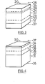
- the diode comprises in sequence a first layer of strongly doped n-type substrate 21, in this case gallium arsenide with an impurity concentration in the range 10 17 to 101 8 cm -3 .
- a second layer of highly doped n-type epitaxial material 22, again gallium arsenide with an impurity concentration in the range 10 17 to 10 18 cm -3 is grown onto the substrate 21.
- the second layer of highly doped n-type material is followed by a third layer of intrinsic material 23, i.e.
- a fourth layer of n-type material 24 gallium arsenide with impurity concentrations in the range 10 16 to 10 17
- a fifth layer 25 of highly doped p-type gallium arsenide with impurity concentra- tions 10 17 to 10 18 .
- Electrical contacts 26 and 27 are made to the fifth layer and to the first layer respectively.
- the special features of the impatt diode illustrated in Fig. 3 are the first Dirac-delta doped monoatomic layer 28 of donors which is present between said second and third layers, and the second Dirac-delta doped monoatomic layer of acceptors 29 present between the fourth and fifth layers 24 and 25 respectively.
- the doping concentrations in the two D 3 layers 28 and 29 lie in the range from 10 to 10 cm -2 and are preferably selected to be 10 13 cm -2 .
- the two layers are grown in the manner described with reference to the field effect transistor of Fig. 1, preferably using silicon for the donors of the layer 28 and berillium for the acceptors of the layer 29.
- the bipolar transistor 30 comprises in sequence a first layer of highly doped n-type substrate 31 (typically GaAs with impurity concentrations in the range 10 17 to 10 18 cm- 3 ), a second layer 32 of n-type material (gallium arsenide with an impurity concentration in the range 10 16 to 10 17 cm -3 ), a third layer of highly doped n-type material 33 (gallium arsenide with an impurity concentration in the range 10 17 to 10 18 ) and a fourth layer of very highly doped n-type material 34 (gallium arsenide with an impurity concentration in the range above 10 18 cm -3 ).
- n-type substrate 31 typically GaAs with impurity concentrations in the range 10 17 to 10 18 cm- 3
- second layer 32 of n-type material gallium arsenide with an impurity concentration in the range 10 16 to 10 17 cm -3
- a third layer of highly doped n-type material 33 gallium arsenide with an impur
- a D 3 monoatomic layer of acceptors having a concentration in the range between 10 11 and 10 14 cm -2 is formed directly between the second and third layers 32, 33.
- the collector contact 36 is formed at the base of the first layer 31.
- the emitter contact 37 is formed on top of the fourth layer 34.
- the base contact 38 is made to the D 3 monoatomic layer 35.
- the transistor 30 has an extremely low base width and a very high cut-off frequency.
- Fig. 5 illustrates an injection laser 40 which is also constructed in accordance with the present invention.
- the laser diode of Fig. 5 has a first layer of a highly doped semiconducting substrate 41, in this case gallium arsenide with a donor concentration in the range 10 17 to 10 18 /cm 3 .
- This first layer 41 is followed by a second layer of a distinct semiconducting material which is also epitaxially grown.
- the second layer 42 consists of highly doped n-type Al x Ga l-x As with a donor concentration in the range 10 17 to 10 18 cm -3 .
- This second layer 42 is followed by a layer of intrinsic semiconducting material of the same type as the substrate, in this case gallium arsenide.
- the layer 43 is then followed by a fourth layer of a highly doped p-type version of the material of the second layer, i.e. A1 x Ga 1-x As with an impurity concentration in the range 10 17 to 10 18 /cm -3 .
- a pair of D 3 monoatomic layers 45 and 46 are provided parallel to one another and spaced apart in said third layer 43.
- the layer 45 is a layer of donors whereas the layer 46 is a layer of acceptors.
- the doping concentrations in these two layers again lie in the range 10 11 to 10 14 cm- 2 .
- the spacing between the two layers lies in the range 25A to 500A.
- the Dirac-delta doping arrangement in the injection laser of Fig. 5 forms two V-shaped potential wells in which the electrons and holes collect.
- the allowed energy states of the electrons and holes are sub-band levels in the V-shaped potential wells. Radiative electron hole transitions occur between the sub-bands of the V-shaped potential wells and generate photons which are radiated out of the device. The generation of these photons is promoted by the voltage applied across the structure via the two contacts 47 and 48 respectively.
- the device is in fact an injection diode. In order to convert it into an injection laser it is necessary to provide one side face with a specularly reflective coating 49 and to provide an opposite parallel side face 50 with a partially reflective coating illustrated by oblique strokes.
- An injection laser or diode of this kind has a high degree of efficiency (quantum efficiency) due to the immediate proximity of the n- and p D 3 layers.
- the operating wavelength can be chosen to be below the wavelength associated with the band gap of the host crystal.
- pronounced carrier confinement occurs in the V-shaped potential wells which leads to low threshold currents for the device.
- the pairs of D 3 layers lie in the active zone of the laser.
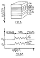
- Fig. 6a there can be seen a schematic diagram of a semiconductor photodetector device.
- the device comprises, in sequence, a first layer of a highly doped n-type semiconducting substrate 53, a second layer of a highly doped n-type semiconducting material 54, a third layer of a distinct intrinsic semiconducting material 55 and a fourth layer of a highly doped n-type semiconducting material 56 similar to said second layer.
- First and second electrical connections are provided to said fourth layer and to said first layer respectively.
- a plurality of pairs of Dirac-delta doped monoatomic layers 57, 57', 58, 58' are provided in said third intrinsic layer 55, with the first Dirac-delta doped monoatomic layer 57, 58 of each pair 57, 57', 58, 58' comprising a monoatomic layer of donors and with the second Dirac-delta doped monoatomic layer 57', 58' of each pair comprising a monoatomic layer of acceptors positioned parallel to and spaced apart from the associated first Dirac-delta doped layer on the side thereof facing said fourth layer.
- the pairs of Dirac-delta doped layers within the intrinsic layer 55 form the STS.
- the first, second and fourth layers are all of gallium arsenide and have respective impurity concentrations of 10 17 -10 19 , 10 17 -10 19 and 10 17 -10 19 cm -3 , respectively.
- the layer 55 consists of GaAs.
- the acceptor and donor concentrations in the D 3 layers again lie in the range 10 11 to 10 14 cm -2 .
- the spacing between sequential D 3 layers is typically 25-250 A and the layers 54, 55 and 56 have respective thicknesses of 0.1-0.5 ⁇ , 0.1-1.0 ⁇ and 0.1-0.5 u.
- Fig. 7 there is shown a schematic illustration of the build-up of an optically bistable device.
- This device comprises a gallium arsenide substrate 60, which may be doped or undoped, and a series of alternating n-type and p-type Dirac-delta doped monoatomic layers 61 to 69 formed on the substrate with each said Dirac-delta doped monoatomic layer being separated from the next adjacent Dirac-delta doped monoatomic layer by a layer of pure undoped intrinsic semiconductor material 70, in this case GaAs.
- the energy band diagram for this optically bistable device is shown in Fig. 7a and the properties of the device may be varied, amongst other things, by varying the separation between the D 3 layers, located in the example of Fig. 7 at zl, z2, z3, z4 etc., which controls the superlattice period length z p and affects the recombination lifetime as described earlier in the introduction to the specification.
Landscapes
- Physics & Mathematics (AREA)
- Optics & Photonics (AREA)
- Engineering & Computer Science (AREA)
- Condensed Matter Physics & Semiconductors (AREA)
- General Physics & Mathematics (AREA)
- Nanotechnology (AREA)
- Electromagnetism (AREA)
- Chemical & Material Sciences (AREA)
- Crystallography & Structural Chemistry (AREA)
- Biophysics (AREA)
- Life Sciences & Earth Sciences (AREA)
- Junction Field-Effect Transistors (AREA)
- Semiconductor Lasers (AREA)
- Led Devices (AREA)
- Light Receiving Elements (AREA)
- Bipolar Transistors (AREA)
- Recrystallisation Techniques (AREA)
Applications Claiming Priority (2)
| Application Number | Priority Date | Filing Date | Title |
|---|---|---|---|
| EP84113987 | 1984-11-19 | ||
| EP84113987 | 1984-11-19 |
Related Child Applications (1)
| Application Number | Title | Priority Date | Filing Date |
|---|---|---|---|
| EP94111989.3 Division-Into | 1985-11-15 |
Publications (3)
| Publication Number | Publication Date |
|---|---|
| EP0183146A2 true EP0183146A2 (de) | 1986-06-04 |
| EP0183146A3 EP0183146A3 (en) | 1989-03-22 |
| EP0183146B1 EP0183146B1 (de) | 1995-04-19 |
Family
ID=8192290
Family Applications (1)
| Application Number | Title | Priority Date | Filing Date |
|---|---|---|---|
| EP85114551A Expired - Lifetime EP0183146B1 (de) | 1984-11-19 | 1985-11-15 | Halbleiteranordnung mit epitaxialem Material |
Country Status (4)
| Country | Link |
|---|---|
| US (1) | US4882609A (de) |
| EP (1) | EP0183146B1 (de) |
| JP (1) | JP2512422B2 (de) |
| DE (1) | DE3588011T2 (de) |
Cited By (14)
| Publication number | Priority date | Publication date | Assignee | Title |
|---|---|---|---|---|
| EP0248439A1 (de) * | 1986-06-06 | 1987-12-09 | AT&T Corp. | Feldeffekttransistor mit einem delta-dotierten ohmschen Kontakt |
| EP0252300A1 (de) * | 1986-06-06 | 1988-01-13 | AT&T Corp. | Ohmsche Metall-Halbleiter-Kontakte |
| EP0199435A3 (en) * | 1985-02-28 | 1988-03-02 | Fujitsu Limited | Field effect semiconductor device |
| FR2618221A1 (fr) * | 1987-07-17 | 1989-01-20 | Thomson Csf | Detecteur d'onde electromagnetique et analyseur d'image comportant un tel detecteur. |
| FR2620268A1 (fr) * | 1987-09-03 | 1989-03-10 | Centre Nat Rech Scient | Procede de dopage d'une couche semi-conductrice et transistor obtenu par ce procede |
| EP0309290A1 (de) * | 1987-09-25 | 1989-03-29 | Nec Corporation | Verbindungshalbleiter-Feldeffekttransistor |
| US4825265A (en) * | 1987-09-04 | 1989-04-25 | American Telephone And Telegraph Company At&T Bell Laboratories | Transistor |
| EP0314836A1 (de) * | 1987-11-06 | 1989-05-10 | Max-Planck-Gesellschaft zur Förderung der Wissenschaften e.V. | Halbleiteranordnung, insbesondere Heiss-Elektronen-Transistor |
| EP0312237A3 (de) * | 1987-10-13 | 1989-10-25 | AT&T Corp. | Anreicherung der Grenzschichtladung in einer delta-dotierten Heterostruktur |
| EP0196245B1 (de) * | 1985-02-22 | 1989-10-25 | Fujitsu Limited | Verbindungshalbleiterschicht mit hoher Trägerkonzentration und Verfahren zu ihrer Herstellung |
| EP0215436B1 (de) * | 1985-09-09 | 1993-03-17 | Sumitomo Electric Industries Limited | Verfahren zum Wachstum einer dünnen Schicht für einen zusammengesetzten Halbleiter |
| DE4235265A1 (de) * | 1992-10-20 | 1994-04-21 | Daimler Benz Ag | Si/SiGe Baritt-Diode |
| EP0784361A1 (de) * | 1995-12-29 | 1997-07-16 | Sharp Kabushiki Kaisha | Halbleiterlaservorrichtung und Herstellungsverfahren |
| EP1231640A4 (de) * | 2000-06-27 | 2008-10-08 | Matsushita Electric Industrial Co Ltd | Halbleiterbauelement |
Families Citing this family (93)
| Publication number | Priority date | Publication date | Assignee | Title |
|---|---|---|---|---|
| US5216260A (en) * | 1984-11-19 | 1993-06-01 | Max-Planck Gesellschaft Zur Foerderung Der Wissenschaften E.V. | Optically bistable semiconductor device with pairs of monoatomic layers separated by intrinsic layers |
| US5060234A (en) * | 1984-11-19 | 1991-10-22 | Max-Planck Gesellschaft Zur Forderung Der Wissenschaften | Injection laser with at least one pair of monoatomic layers of doping atoms |
| JPH0738460B2 (ja) * | 1985-12-27 | 1995-04-26 | オムロン株式会社 | 半導体発光素子 |
| US5497015A (en) * | 1988-11-12 | 1996-03-05 | Sony Corporation | Quantum interference transistor |
| US5013685A (en) * | 1989-11-02 | 1991-05-07 | At&T Bell Laboratories | Method of making a non-alloyed ohmic contact to III-V semiconductors-on-silicon |
| US5081511A (en) * | 1990-09-06 | 1992-01-14 | Motorola, Inc. | Heterojunction field effect transistor with monolayers in channel region |
| US5206527A (en) * | 1990-11-09 | 1993-04-27 | Sumitomo Electric Industries, Ltd. | Field effect transistor |
| JP2549206B2 (ja) * | 1990-12-27 | 1996-10-30 | 住友電気工業株式会社 | 電界効果トランジスタ |
| US5151758A (en) * | 1991-02-20 | 1992-09-29 | Comsat | Planar-doped valley field effect transistor (PDVFET) |
| US5219772A (en) * | 1991-08-15 | 1993-06-15 | At&T Bell Laboratories | Method for making field effect devices with ultra-short gates |
| KR940006711B1 (ko) * | 1991-09-12 | 1994-07-25 | 포항종합제철 주식회사 | 델타도핑 양자 우물전계 효과 트랜지스터의 제조방법 |
| JPH05291307A (ja) * | 1991-12-05 | 1993-11-05 | Samsung Electron Co Ltd | 化合物半導体装置及びその製造方法 |
| JPH0817231B2 (ja) * | 1992-01-29 | 1996-02-21 | 東京工業大学長 | 組織ドープ構造半導体装置 |
| FR2691839B1 (fr) * | 1992-05-27 | 1994-08-05 | Schlumberger Ind Sa | Capteur a effet hall. |
| US5376810A (en) * | 1992-06-26 | 1994-12-27 | California Institute Of Technology | Growth of delta-doped layers on silicon CCD/S for enhanced ultraviolet response |
| JPH06104289A (ja) * | 1992-09-18 | 1994-04-15 | Hitachi Ltd | 半導体装置およびそれを用いた増幅回路 |
| KR960004594B1 (ko) * | 1993-03-17 | 1996-04-09 | 엘지전자주식회사 | 적외선 광 검출기 |
| US5432119A (en) * | 1994-01-31 | 1995-07-11 | Hughes Aircraft Company | High yield electron-beam gate fabrication method for sub-micron gate FETS |
| US5569943A (en) * | 1995-09-01 | 1996-10-29 | The United States Of America As Represented By The Secretary Of The Army | Field effect real space transistor |
| EP0841704A1 (de) * | 1996-11-07 | 1998-05-13 | Paul-Drude-Institut für Festkörperelektronik | Transistorhalbleiterbauelement und Verfahren zu dessen Herstellung |
| JP3458349B2 (ja) * | 1996-11-19 | 2003-10-20 | 株式会社デンソー | 半導体装置 |
| US6258616B1 (en) * | 1998-05-22 | 2001-07-10 | Lucent Technologies Inc. | Method of making a semiconductor device having a non-alloyed ohmic contact to a buried doped layer |
| US6993222B2 (en) * | 1999-03-03 | 2006-01-31 | Rj Mears, Llc | Optical filter device with aperiodically arranged grating elements |
| GB2385940B (en) | 1999-03-05 | 2003-10-22 | Nanovis Llc | Aperiodically poled non-linear material |
| ATE355615T1 (de) * | 2000-03-03 | 2006-03-15 | Matsushita Electric Industrial Co Ltd | Halbleiteranordnung |
| EP1684359A3 (de) * | 2000-05-31 | 2006-10-25 | Matsushita Electrical Industrial Co., Ltd | Misfet |
| TWI288435B (en) | 2000-11-21 | 2007-10-11 | Matsushita Electric Industrial Co Ltd | Semiconductor device and equipment for communication system |
| DE60234944D1 (de) * | 2001-09-27 | 2010-02-11 | Merck & Co Inc | Isolierte dna-moleküle, die für einen humanisierten calcitonin gene-related peptide receptor kodiered assayverfahren |
| JP4463482B2 (ja) * | 2002-07-11 | 2010-05-19 | パナソニック株式会社 | Misfet及びその製造方法 |
| CA2495309C (en) * | 2002-08-13 | 2011-11-08 | Massachusetts Institute Of Technology | Semiconductor nanocrystal heterostructures |
| US20060292765A1 (en) * | 2003-06-26 | 2006-12-28 | Rj Mears, Llc | Method for Making a FINFET Including a Superlattice |
| US7514328B2 (en) * | 2003-06-26 | 2009-04-07 | Mears Technologies, Inc. | Method for making a semiconductor device including shallow trench isolation (STI) regions with a superlattice therebetween |
| US20060231857A1 (en) * | 2003-06-26 | 2006-10-19 | Rj Mears, Llc | Method for making a semiconductor device including a memory cell with a negative differential resistance (ndr) device |
| US7586165B2 (en) * | 2003-06-26 | 2009-09-08 | Mears Technologies, Inc. | Microelectromechanical systems (MEMS) device including a superlattice |
| US20070063186A1 (en) * | 2003-06-26 | 2007-03-22 | Rj Mears, Llc | Method for making a semiconductor device including a front side strained superlattice layer and a back side stress layer |
| US20060243964A1 (en) * | 2003-06-26 | 2006-11-02 | Rj Mears, Llc | Method for making a semiconductor device having a semiconductor-on-insulator configuration and a superlattice |
| US7598515B2 (en) * | 2003-06-26 | 2009-10-06 | Mears Technologies, Inc. | Semiconductor device including a strained superlattice and overlying stress layer and related methods |
| US20040266116A1 (en) * | 2003-06-26 | 2004-12-30 | Rj Mears, Llc | Methods of fabricating semiconductor structures having improved conductivity effective mass |
| US7045813B2 (en) * | 2003-06-26 | 2006-05-16 | Rj Mears, Llc | Semiconductor device including a superlattice with regions defining a semiconductor junction |
| US20060220118A1 (en) * | 2003-06-26 | 2006-10-05 | Rj Mears, Llc | Semiconductor device including a dopant blocking superlattice |
| US7531850B2 (en) * | 2003-06-26 | 2009-05-12 | Mears Technologies, Inc. | Semiconductor device including a memory cell with a negative differential resistance (NDR) device |
| US20050279991A1 (en) * | 2003-06-26 | 2005-12-22 | Rj Mears, Llc | Semiconductor device including a superlattice having at least one group of substantially undoped layers |
| US7531828B2 (en) * | 2003-06-26 | 2009-05-12 | Mears Technologies, Inc. | Semiconductor device including a strained superlattice between at least one pair of spaced apart stress regions |
| US20050282330A1 (en) * | 2003-06-26 | 2005-12-22 | Rj Mears, Llc | Method for making a semiconductor device including a superlattice having at least one group of substantially undoped layers |
| US7659539B2 (en) | 2003-06-26 | 2010-02-09 | Mears Technologies, Inc. | Semiconductor device including a floating gate memory cell with a superlattice channel |
| US20060011905A1 (en) * | 2003-06-26 | 2006-01-19 | Rj Mears, Llc | Semiconductor device comprising a superlattice dielectric interface layer |
| US7227174B2 (en) * | 2003-06-26 | 2007-06-05 | Rj Mears, Llc | Semiconductor device including a superlattice and adjacent semiconductor layer with doped regions defining a semiconductor junction |
| US20070020833A1 (en) * | 2003-06-26 | 2007-01-25 | Rj Mears, Llc | Method for Making a Semiconductor Device Including a Channel with a Non-Semiconductor Layer Monolayer |
| US7535041B2 (en) * | 2003-06-26 | 2009-05-19 | Mears Technologies, Inc. | Method for making a semiconductor device including regions of band-engineered semiconductor superlattice to reduce device-on resistance |
| US20070010040A1 (en) * | 2003-06-26 | 2007-01-11 | Rj Mears, Llc | Method for Making a Semiconductor Device Including a Strained Superlattice Layer Above a Stress Layer |
| US7153763B2 (en) | 2003-06-26 | 2006-12-26 | Rj Mears, Llc | Method for making a semiconductor device including band-engineered superlattice using intermediate annealing |
| US7586116B2 (en) * | 2003-06-26 | 2009-09-08 | Mears Technologies, Inc. | Semiconductor device having a semiconductor-on-insulator configuration and a superlattice |
| US20070063185A1 (en) * | 2003-06-26 | 2007-03-22 | Rj Mears, Llc | Semiconductor device including a front side strained superlattice layer and a back side stress layer |
| US7045377B2 (en) * | 2003-06-26 | 2006-05-16 | Rj Mears, Llc | Method for making a semiconductor device including a superlattice and adjacent semiconductor layer with doped regions defining a semiconductor junction |
| US20040262594A1 (en) * | 2003-06-26 | 2004-12-30 | Rj Mears, Llc | Semiconductor structures having improved conductivity effective mass and methods for fabricating same |
| US7491587B2 (en) * | 2003-06-26 | 2009-02-17 | Mears Technologies, Inc. | Method for making a semiconductor device having a semiconductor-on-insulator (SOI) configuration and including a superlattice on a thin semiconductor layer |
| US20060267130A1 (en) * | 2003-06-26 | 2006-11-30 | Rj Mears, Llc | Semiconductor Device Including Shallow Trench Isolation (STI) Regions with a Superlattice Therebetween |
| US20070020860A1 (en) * | 2003-06-26 | 2007-01-25 | Rj Mears, Llc | Method for Making Semiconductor Device Including a Strained Superlattice and Overlying Stress Layer and Related Methods |
| US7202494B2 (en) * | 2003-06-26 | 2007-04-10 | Rj Mears, Llc | FINFET including a superlattice |
| US20070015344A1 (en) * | 2003-06-26 | 2007-01-18 | Rj Mears, Llc | Method for Making a Semiconductor Device Including a Strained Superlattice Between at Least One Pair of Spaced Apart Stress Regions |
| US7531829B2 (en) * | 2003-06-26 | 2009-05-12 | Mears Technologies, Inc. | Semiconductor device including regions of band-engineered semiconductor superlattice to reduce device-on resistance |
| US6833294B1 (en) * | 2003-06-26 | 2004-12-21 | Rj Mears, Llc | Method for making semiconductor device including band-engineered superlattice |
| US6958486B2 (en) * | 2003-06-26 | 2005-10-25 | Rj Mears, Llc | Semiconductor device including band-engineered superlattice |
| US7229902B2 (en) * | 2003-06-26 | 2007-06-12 | Rj Mears, Llc | Method for making a semiconductor device including a superlattice with regions defining a semiconductor junction |
| US20060289049A1 (en) * | 2003-06-26 | 2006-12-28 | Rj Mears, Llc | Semiconductor Device Having a Semiconductor-on-Insulator (SOI) Configuration and Including a Superlattice on a Thin Semiconductor Layer |
| EP1644983B1 (de) * | 2003-06-26 | 2008-10-29 | Mears Technologies, Inc. | Halbleiterbauelement mit einem mosfet mit bandlücken-angepasstem übergitter |
| US7612366B2 (en) * | 2003-06-26 | 2009-11-03 | Mears Technologies, Inc. | Semiconductor device including a strained superlattice layer above a stress layer |
| US20060273299A1 (en) * | 2003-06-26 | 2006-12-07 | Rj Mears, Llc | Method for making a semiconductor device including a dopant blocking superlattice |
| US7446002B2 (en) * | 2003-06-26 | 2008-11-04 | Mears Technologies, Inc. | Method for making a semiconductor device comprising a superlattice dielectric interface layer |
| US20070158640A1 (en) * | 2005-12-22 | 2007-07-12 | Rj Mears, Llc | Electronic device including a poled superlattice having a net electrical dipole moment |
| US7517702B2 (en) * | 2005-12-22 | 2009-04-14 | Mears Technologies, Inc. | Method for making an electronic device including a poled superlattice having a net electrical dipole moment |
| US7394094B2 (en) * | 2005-12-29 | 2008-07-01 | Massachusetts Institute Of Technology | Semiconductor nanocrystal heterostructures |
| US7718996B2 (en) * | 2006-02-21 | 2010-05-18 | Mears Technologies, Inc. | Semiconductor device comprising a lattice matching layer |
| WO2008023821A1 (fr) * | 2006-08-25 | 2008-02-28 | National Institute For Materials Science | Semi-conducteur et son procédé de production |
| US7483212B2 (en) * | 2006-10-11 | 2009-01-27 | Rensselaer Polytechnic Institute | Optical thin film, semiconductor light emitting device having the same and methods of fabricating the same |
| US7781827B2 (en) | 2007-01-24 | 2010-08-24 | Mears Technologies, Inc. | Semiconductor device with a vertical MOSFET including a superlattice and related methods |
| US7928425B2 (en) * | 2007-01-25 | 2011-04-19 | Mears Technologies, Inc. | Semiconductor device including a metal-to-semiconductor superlattice interface layer and related methods |
| US7863066B2 (en) * | 2007-02-16 | 2011-01-04 | Mears Technologies, Inc. | Method for making a multiple-wavelength opto-electronic device including a superlattice |
| US7880161B2 (en) * | 2007-02-16 | 2011-02-01 | Mears Technologies, Inc. | Multiple-wavelength opto-electronic device including a superlattice |
| US7812339B2 (en) * | 2007-04-23 | 2010-10-12 | Mears Technologies, Inc. | Method for making a semiconductor device including shallow trench isolation (STI) regions with maskless superlattice deposition following STI formation and related structures |
| KR101018088B1 (ko) * | 2008-11-07 | 2011-02-25 | 삼성엘이디 주식회사 | 질화물 반도체 소자 |
| EP3011594B1 (de) * | 2013-06-20 | 2018-12-26 | Stratio, Inc. | Gategesteuerte ladungsmodulierte vorrichtung für cmos-bildsensoren |
| US9166035B2 (en) * | 2013-09-12 | 2015-10-20 | Taiwan Semiconductor Manufacturing Company Limited | Delta doping layer in MOSFET source/drain region |
| US9406753B2 (en) | 2013-11-22 | 2016-08-02 | Atomera Incorporated | Semiconductor devices including superlattice depletion layer stack and related methods |
| KR101855023B1 (ko) | 2013-11-22 | 2018-05-04 | 아토메라 인코포레이티드 | 정지층을 통한 초격자 펀치를 포함하는 수직 반도체 디바이스 및 관련된 방법 |
| US9716147B2 (en) | 2014-06-09 | 2017-07-25 | Atomera Incorporated | Semiconductor devices with enhanced deterministic doping and related methods |
| US9722046B2 (en) | 2014-11-25 | 2017-08-01 | Atomera Incorporated | Semiconductor device including a superlattice and replacement metal gate structure and related methods |
| WO2016187038A1 (en) | 2015-05-15 | 2016-11-24 | Atomera Incorporated | Semiconductor devices with superlattice and punch-through stop (pts) layers at different depths and related methods |
| WO2016196600A1 (en) | 2015-06-02 | 2016-12-08 | Atomera Incorporated | Method for making enhanced semiconductor structures in single wafer processing chamber with desired uniformity control |
| US9558939B1 (en) | 2016-01-15 | 2017-01-31 | Atomera Incorporated | Methods for making a semiconductor device including atomic layer structures using N2O as an oxygen source |
| US9927461B2 (en) * | 2016-03-09 | 2018-03-27 | Mark J. Hagmann | Apparatus and algorithm for carrier profiling in scanning frequency comb microscopy |
| DE102020213957B3 (de) | 2020-11-06 | 2021-09-30 | Fraunhofer-Gesellschaft zur Förderung der angewandten Forschung eingetragener Verein | Fotoleiter und verfahren zu dessen herstellung |
| CN112670356B (zh) * | 2020-12-24 | 2023-05-12 | 湖南科莱特光电有限公司 | 单分子层内δ掺杂的半导体材料及其制备方法和探测器 |
Family Cites Families (9)
| Publication number | Priority date | Publication date | Assignee | Title |
|---|---|---|---|---|
| DE2261527C2 (de) * | 1972-12-15 | 1983-04-21 | Max-Planck-Gesellschaft zur Förderung der Wissenschaften e.V., 3400 Göttingen | Halbleiterkörper mit in einer vorgegebenen Richtung abwechselnd aufeinanderfolgenden n- und p-dotierten Zonen, Verfahren zu seiner Herstellung und Verwendungen des Halbleiterkörpers |
| US4205329A (en) * | 1976-03-29 | 1980-05-27 | Bell Telephone Laboratories, Incorporated | Periodic monolayer semiconductor structures grown by molecular beam epitaxy |
| US4163237A (en) * | 1978-04-24 | 1979-07-31 | Bell Telephone Laboratories, Incorporated | High mobility multilayered heterojunction devices employing modulated doping |
| US4410902A (en) * | 1981-03-23 | 1983-10-18 | The United States Of America As Represented By The Secretary Of The Army | Planar doped barrier semiconductor device |
| US4525731A (en) * | 1982-12-30 | 1985-06-25 | International Business Machines Corporation | Semiconductor conversion of optical-to-electrical energy |
| US4504846A (en) * | 1982-12-30 | 1985-03-12 | International Business Machines Corporation | Multiwavelength optical-to-electrical logic operations |
| JPS60117680A (ja) * | 1983-11-29 | 1985-06-25 | Nippon Telegr & Teleph Corp <Ntt> | 高速電界効果トランジスタ |
| ZA849070B (en) * | 1983-12-07 | 1985-07-31 | Energy Conversion Devices Inc | Semiconducting multilayered structures and systems and methods for synthesizing the structures and devices incorporating the structures |
| US4591889A (en) * | 1984-09-14 | 1986-05-27 | At&T Bell Laboratories | Superlattice geometry and devices |
-
1985
- 1985-11-14 US US06/798,053 patent/US4882609A/en not_active Expired - Fee Related
- 1985-11-15 EP EP85114551A patent/EP0183146B1/de not_active Expired - Lifetime
- 1985-11-15 DE DE3588011T patent/DE3588011T2/de not_active Expired - Fee Related
- 1985-11-19 JP JP25963185A patent/JP2512422B2/ja not_active Expired - Lifetime
Cited By (20)
| Publication number | Priority date | Publication date | Assignee | Title |
|---|---|---|---|---|
| EP0196245B1 (de) * | 1985-02-22 | 1989-10-25 | Fujitsu Limited | Verbindungshalbleiterschicht mit hoher Trägerkonzentration und Verfahren zu ihrer Herstellung |
| EP0199435A3 (en) * | 1985-02-28 | 1988-03-02 | Fujitsu Limited | Field effect semiconductor device |
| US4833508A (en) * | 1985-02-28 | 1989-05-23 | Fujitsu Limited | High electron mobility device with intrinsic AlAs/GaAs superlattice separator region |
| EP0215436B1 (de) * | 1985-09-09 | 1993-03-17 | Sumitomo Electric Industries Limited | Verfahren zum Wachstum einer dünnen Schicht für einen zusammengesetzten Halbleiter |
| EP0252300A1 (de) * | 1986-06-06 | 1988-01-13 | AT&T Corp. | Ohmsche Metall-Halbleiter-Kontakte |
| EP0248439A1 (de) * | 1986-06-06 | 1987-12-09 | AT&T Corp. | Feldeffekttransistor mit einem delta-dotierten ohmschen Kontakt |
| US4878095A (en) * | 1987-06-11 | 1989-10-31 | Wissenschaften E.V. | Semiconductor device in particular a hot electron transistor |
| FR2618221A1 (fr) * | 1987-07-17 | 1989-01-20 | Thomson Csf | Detecteur d'onde electromagnetique et analyseur d'image comportant un tel detecteur. |
| EP0299841A3 (en) * | 1987-07-17 | 1989-04-12 | Thomson-Csf | Electromagnetic wave detector and image analyser using such a detector |
| US5160991A (en) * | 1987-07-17 | 1992-11-03 | Thomson-Csf | Electromagnetic wave detector and image analyzer comprising a detector of this type |
| FR2620268A1 (fr) * | 1987-09-03 | 1989-03-10 | Centre Nat Rech Scient | Procede de dopage d'une couche semi-conductrice et transistor obtenu par ce procede |
| EP0306258A3 (en) * | 1987-09-04 | 1989-10-18 | American Telephone And Telegraph Company | Transistor |
| US4825265A (en) * | 1987-09-04 | 1989-04-25 | American Telephone And Telegraph Company At&T Bell Laboratories | Transistor |
| EP0309290A1 (de) * | 1987-09-25 | 1989-03-29 | Nec Corporation | Verbindungshalbleiter-Feldeffekttransistor |
| EP0312237A3 (de) * | 1987-10-13 | 1989-10-25 | AT&T Corp. | Anreicherung der Grenzschichtladung in einer delta-dotierten Heterostruktur |
| EP0314836A1 (de) * | 1987-11-06 | 1989-05-10 | Max-Planck-Gesellschaft zur Förderung der Wissenschaften e.V. | Halbleiteranordnung, insbesondere Heiss-Elektronen-Transistor |
| DE4235265A1 (de) * | 1992-10-20 | 1994-04-21 | Daimler Benz Ag | Si/SiGe Baritt-Diode |
| EP0784361A1 (de) * | 1995-12-29 | 1997-07-16 | Sharp Kabushiki Kaisha | Halbleiterlaservorrichtung und Herstellungsverfahren |
| US5828685A (en) * | 1995-12-29 | 1998-10-27 | Sharp Kabushiki Kaisha | Semiconductor laser device and a method of growing a semiconductor laser device |
| EP1231640A4 (de) * | 2000-06-27 | 2008-10-08 | Matsushita Electric Industrial Co Ltd | Halbleiterbauelement |
Also Published As
| Publication number | Publication date |
|---|---|
| EP0183146B1 (de) | 1995-04-19 |
| DE3588011T2 (de) | 1995-08-31 |
| JP2512422B2 (ja) | 1996-07-03 |
| JPS61166081A (ja) | 1986-07-26 |
| US4882609A (en) | 1989-11-21 |
| DE3588011D1 (de) | 1995-05-24 |
| EP0183146A3 (en) | 1989-03-22 |
Similar Documents
| Publication | Publication Date | Title |
|---|---|---|
| US5060234A (en) | Injection laser with at least one pair of monoatomic layers of doping atoms | |
| US4882609A (en) | Semiconductor devices with at least one monoatomic layer of doping atoms | |
| Ploog et al. | Fundamental studies and device application of δ-doping in GaAs Layers and in AlxGa1− xAs/GaAs heterostructures | |
| US4686550A (en) | Heterojunction semiconductor devices having a doping interface dipole | |
| Ploog | Delta-(-) doping in MBE-grown GaAs: concept and device application | |
| US5281543A (en) | Fabrication method for quantum devices in compound semiconductor layers | |
| EP0494395B1 (de) | Feldeffekttransistor mit geneigtem Kanal | |
| US5495115A (en) | Semiconductor crystalline laminate structure, forming method of the same, and semiconductor device employing the same | |
| EP0312237A2 (de) | Anreicherung der Grenzschichtladung in einer delta-dotierten Heterostruktur | |
| US5436468A (en) | Ordered mixed crystal semiconductor superlattice device | |
| JP2500063B2 (ja) | 電界効果トランジスタ | |
| US4959696A (en) | Three terminal tunneling device and method | |
| Döhler | The physics and applications of nipi doping superlattices | |
| EP0632504B1 (de) | Halbleitervorrichtung mit Gradienten-Bandabstand BeTe-ZnSe ohmschem Kontakt für einen II-VI Halbleiter | |
| US5012301A (en) | Three terminal semiconductor device | |
| US5216260A (en) | Optically bistable semiconductor device with pairs of monoatomic layers separated by intrinsic layers | |
| US4851886A (en) | Binary superlattice tunneling device and method | |
| EP0205164B1 (de) | Struktur einer Halbleiteranordnung | |
| EP0405832B1 (de) | Dotierungsverfahren für Halbleiterbauelemente | |
| EP0352019B1 (de) | Modulationsvorrichtung für optische Kommunikationstechnik | |
| EP0197052B1 (de) | Eine neue halbleiteranordnung | |
| Ginoudi et al. | Low‐temperature dc characteristics of S‐and Si‐doped Ga0. 51In0. 49P/GaAs high electron mobility transistors grown by metalorganic molecular beam epitaxy | |
| EP0268386A2 (de) | Tunneltransistor | |
| Sealy | Review of III-V semiconductor materials and devices | |
| EP0697741A1 (de) | Anordnungen mit resonantem Tunneleffekt |
Legal Events
| Date | Code | Title | Description |
|---|---|---|---|
| PUAI | Public reference made under article 153(3) epc to a published international application that has entered the european phase |
Free format text: ORIGINAL CODE: 0009012 |
|
| AK | Designated contracting states |
Kind code of ref document: A2 Designated state(s): DE FR GB IT NL |
|
| RHK1 | Main classification (correction) |
Ipc: H01L 29/36 |
|
| RHK1 | Main classification (correction) |
Ipc: H01L 29/205 |
|
| PUAL | Search report despatched |
Free format text: ORIGINAL CODE: 0009013 |
|
| AK | Designated contracting states |
Kind code of ref document: A3 Designated state(s): DE FR GB IT NL |
|
| 17P | Request for examination filed |
Effective date: 19890918 |
|
| 17Q | First examination report despatched |
Effective date: 19901023 |
|
| GRAA | (expected) grant |
Free format text: ORIGINAL CODE: 0009210 |
|
| AK | Designated contracting states |
Kind code of ref document: B1 Designated state(s): DE FR GB IT NL |
|
| PG25 | Lapsed in a contracting state [announced via postgrant information from national office to epo] |
Ref country code: IT Free format text: LAPSE BECAUSE OF FAILURE TO SUBMIT A TRANSLATION OF THE DESCRIPTION OR TO PAY THE FEE WITHIN THE PRESCRIBED TIME-LIMIT;WARNING: LAPSES OF ITALIAN PATENTS WITH EFFECTIVE DATE BEFORE 2007 MAY HAVE OCCURRED AT ANY TIME BEFORE 2007. THE CORRECT EFFECTIVE DATE MAY BE DIFFERENT FROM THE ONE RECORDED. Effective date: 19950419 |
|
| XX | Miscellaneous (additional remarks) |
Free format text: TEILANMELDUNG 94111989.3 EINGEREICHT AM 15/11/85. |
|
| ET | Fr: translation filed | ||
| REF | Corresponds to: |
Ref document number: 3588011 Country of ref document: DE Date of ref document: 19950524 |
|
| PG25 | Lapsed in a contracting state [announced via postgrant information from national office to epo] |
Ref country code: GB Effective date: 19951115 |
|
| PLBE | No opposition filed within time limit |
Free format text: ORIGINAL CODE: 0009261 |
|
| STAA | Information on the status of an ep patent application or granted ep patent |
Free format text: STATUS: NO OPPOSITION FILED WITHIN TIME LIMIT |
|
| 26N | No opposition filed | ||
| PG25 | Lapsed in a contracting state [announced via postgrant information from national office to epo] |
Ref country code: NL Effective date: 19960601 |
|
| GBPC | Gb: european patent ceased through non-payment of renewal fee |
Effective date: 19951115 |
|
| PG25 | Lapsed in a contracting state [announced via postgrant information from national office to epo] |
Ref country code: FR Effective date: 19960731 |
|
| NLV4 | Nl: lapsed or anulled due to non-payment of the annual fee |
Effective date: 19960601 |
|
| PG25 | Lapsed in a contracting state [announced via postgrant information from national office to epo] |
Ref country code: DE Effective date: 19960801 |
|
| REG | Reference to a national code |
Ref country code: FR Ref legal event code: ST |