EP0312237A2 - Anreicherung der Grenzschichtladung in einer delta-dotierten Heterostruktur - Google Patents
Anreicherung der Grenzschichtladung in einer delta-dotierten Heterostruktur Download PDFInfo
- Publication number
- EP0312237A2 EP0312237A2 EP88309251A EP88309251A EP0312237A2 EP 0312237 A2 EP0312237 A2 EP 0312237A2 EP 88309251 A EP88309251 A EP 88309251A EP 88309251 A EP88309251 A EP 88309251A EP 0312237 A2 EP0312237 A2 EP 0312237A2
- Authority
- EP
- European Patent Office
- Prior art keywords
- semiconductor
- layer
- material composition
- semiconductor structure
- heterointerface
- Prior art date
- Legal status (The legal status is an assumption and is not a legal conclusion. Google has not performed a legal analysis and makes no representation as to the accuracy of the status listed.)
- Withdrawn
Links
Images

Classifications
-
- H—ELECTRICITY
- H10—SEMICONDUCTOR DEVICES; ELECTRIC SOLID-STATE DEVICES NOT OTHERWISE PROVIDED FOR
- H10D—INORGANIC ELECTRIC SEMICONDUCTOR DEVICES
- H10D30/00—Field-effect transistors [FET]
- H10D30/40—FETs having zero-dimensional [0D], one-dimensional [1D] or two-dimensional [2D] charge carrier gas channels
- H10D30/47—FETs having zero-dimensional [0D], one-dimensional [1D] or two-dimensional [2D] charge carrier gas channels having two-dimensional [2D] charge carrier gas channels, e.g. nanoribbon FETs or high electron mobility transistors [HEMT]
- H10D30/471—High electron mobility transistors [HEMT] or high hole mobility transistors [HHMT]
- H10D30/475—High electron mobility transistors [HEMT] or high hole mobility transistors [HHMT] having wider bandgap layer formed on top of lower bandgap active layer, e.g. undoped barrier HEMTs such as i-AlGaN/GaN HEMTs
- H10D30/4755—High electron mobility transistors [HEMT] or high hole mobility transistors [HHMT] having wider bandgap layer formed on top of lower bandgap active layer, e.g. undoped barrier HEMTs such as i-AlGaN/GaN HEMTs having wide bandgap charge-carrier supplying layers, e.g. modulation doped HEMTs such as n-AlGaAs/GaAs HEMTs
-
- H—ELECTRICITY
- H10—SEMICONDUCTOR DEVICES; ELECTRIC SOLID-STATE DEVICES NOT OTHERWISE PROVIDED FOR
- H10D—INORGANIC ELECTRIC SEMICONDUCTOR DEVICES
- H10D62/00—Semiconductor bodies, or regions thereof, of devices having potential barriers
- H10D62/60—Impurity distributions or concentrations
- H10D62/605—Planar doped, e.g. atomic-plane doped or delta-doped
Definitions
- This invention relates to the field of semiconductor devices and, more particularly, to devices including a delta-doped layer.
- semiconductor layer growth is begun on an intrinsic or semi-insulating Group III-V material substrate such as GaAs.
- An undoped channel layer of GaAs is grown to a thickness of approximately 1 ⁇ m.
- the first A1GaAs layer is an undoped spacer layer having a thickness of approximately 0 to 200 Angstroms.
- This layer is then overgrown by a uniformly doped (n-type or p- type) A1GaAs layer approximately 500 Angstroms thick.
- An undoped GaAs contact layer (approximately 100 Angstrom thickness) completes the semiconductor heterostructure growth.
- heterostructures of the type described above incorporated in devices such as field effect transistors suffer a critical degradation in carrier mobilities for interface electron densities (two dimensional electron gas densities) in excess of approximately 1 x 1012 cm ⁇ 2. It is also known that there is a potential drop in the depletion region for these devices which occurs from impurity atoms in the uniformly doped layer.
- Electron mobility is preserved and the two dimensional electron gas concentration or interface charge density is significantly increased over that for known semiconductor structures by incorporating an atomic planar doping layer (delta-doped layer) in close proximity to a heterointerface such that a spacer semiconductor layer separates the atomic planar doping layer from the heterointerface.
- the doping concentration of the atomic planar doping layer is selected to cause a selected barrier thickness for charge carriers in the conduction band of the atomic planar doping layer to be less than the spacer thickness.
- the two-dimensional electron gas density is caused to exceed known device limits for homogeneously doped structures while maintaining a relatively high mobility.
- high transconductances are achieved for field effect transistor devices utilizing the atomic planar doping layer closely proximate the heterointerface.
- a delta-doped layer within a quantum well layer is included in the heterostructure to reduce persistent photoconductivity resulting from deep donors.
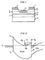
- FIG. 1 shows in cross-sectional view a schematic diagram of a conventional selectively doped heterostructure field effect transistor.
- the field effect transistor is comprised of Group III-V semiconductor materials and, more particularly, materials selected from the AlGaAs/GaAs system.
- the selectively doped heterostructure field effect transistor generally includes an undoped or semi-insulating GaAs substrate 10 upon which is grown the following sequence of layers: an undoped GaAs channel layer 11, an undoped AlGaAs spacer layer 12, a doped AlGaAs donor layer 13, and doped GaAs cap layers 14. Standard photolithographic techniques and chemical etching are used to create a gate recess to accommodate a gate contact over the channel layer.
- Metallic contacts 15 and 17 are formed over the source and drain regions respectively, and are ohmic in nature.
- Metallic contact 16 is formed over the gate region and is typically a Schottky barrier contact.
- channel layer 11 is less than 1.0 ⁇ m. in thickness; spacer layer 12 is approximately 20-80 Angstroms thick; donor layer 13 is approximately 300-500 Angstroms thick with a dopant concentration of approximately 1018cm ⁇ 2 for Si; and cap layer 14 has a thickness between 0-500 Angstroms with a dopant concentration similar to that for layer 13.
- the two-dimensional electron gas density falls in the range 0.5 to 1.5x 1012cm ⁇ 2.
- Dashed line 18 depicts the location of two-dimensional electron gas within the device.
- g m dI ds /dV g
- FIG. 2 shows an energy band diagram for the heterostructure shown in FIG. 1.
- E F , E C and E V represent the Ferni, conduction and valence energies, respectively.
- Dashed line 20 represents the heterointerface between layers 11 and 12 in FIG. 1.
- the two-dimensional electron gas layer is represented by hatched area 21.
- Spacer layer thickness is represented as W s .
- V D is the potential drop in the depletion region (qV D is the energy) and V s represents the potential drop across the spacer layer.
- Baud shape is determined by homogeneously and uniformly doping layers 13 and 14.
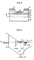
- FIG. 3 shows in cross-sectional view a selectively doped heterostructure field effect transistor including a delta-doped layer 32 in close proximity to the heterointerface between channel layer 31 and spacer layer 32.
- the transistor includes a semi-insulating or intrinsic GaAs substrate layer 30 upon which is epitaxially grown the following sequence of layers: undoped GaAs channel layer 31; undoped AlGaAs spacer layer 32; delta-doping layer 33; doped AlGaAs donor layer 34; and doped GaAs cap layers 35.
- Source contact 36, drain contact 38 and gate contact 37 are metallic contacts. Fabrication techniques are substantially identical to those employed for the device shown in FIG. 1.
- Heterostructures such as shown in FIG. 3 have been grown in a Varian Generator V80 gas source molecular beam epitaxy system. This is a horizontal growth chamber equipped with conventional Group III sources. Arsenic flux has been provided by thermally decomposed arsine.
- Channel layer 31 is approximately 1.0 ⁇ m thick; the AlGaAs spacer layer 32 is grown to a thickness between 0 and 100 Angstroms.
- Donor layer 34 and cap layer 35 are then grown to conventional thicknesses and carrier concentrations.
- delta-doping layer 33 be grown within spacer layer 32 by interrupting the growth of layer 32 with an intervening, precalibrated, submonolayer dopant (Si for n-type) dose substantially at a distance W s from the heterointerface. Growth of the remaining portion of layer 32 is then resumed to completion over delta doping layer 33. For this structure, growth of donor layer 34 follows over layer 32 including layer 33. The thickness for entire layer 32 in this structure is substantially in the range of 0 to 1000 Angstroms.
- the transistor shown in FIG. 3 has been fabricated with a gate width of 150 ⁇ m, a gate length of 1.2 ⁇ m and a source-to-drain spacing of 4.0 ⁇ m.
- Contacts for the device were comprised of alloyed multilayer ohmic (source and drain) contacts and a multilayer Schottky (gate) contact.
- the ohmic contact included layers of 2000 Angstroms AuGe (eutectic), 400 Angstroms Ni and 2000 Angstroms Au; the Schottky contact was comprised of layers of 500 Angstroms Ti and 1500 Angstroms Au.
- FIG. 4 shows an energy band diagram for the device substantially as described in FIG. 3.
- the potential well in the conduction band is of sufficient strength, because of the high delta doping concentration, to quantize electrons (holes for p-type) into individual subands at eigenstate energies E0 through E n where for h as Planck's constant, m* is the effective electron mass, q is the effective element charge, ⁇ is the permittivity and N is the corresponding delta doping concentration.
- This quantization reduces the selected barrier thickness below the spacer thickness, W s . It should be clear from the diagram that the selected barrier thickness is measured from a conduction band edge of the lowest order eigenstate (filled conduction subband) to the heterointerface.
- Region 42 shows subband filling of the lowest eigenstate E0 in the substantially sharp v-shaped potential well caused by delta doping.
- cross-hatched regions 43 and 44 represent lowest order eigenstates in the conduction channel.
- the substantially sharp v-shaped potential well caused by the delta doping layer induces a concomitant quantum size effect thereby permitting the selected barrier thickness seen by electrons in region 42 to be less than the spacer layer thickness, W s .
- the potential drop V D is not present in FIG. 4 because of the localization of donor impurities caused by delta doping.
- the two-dimensional electron gas density positioned approximately at dashed line 39 is nearly two times larger for the present delta doping layer structure over conventional devices having comparable spacer thicknesses, W s .
- W s spacer thicknesses
- curves 50 and 51 refer to conventional uniformly doped heterostructures having doping concentrations of 1018 and ⁇ cm ⁇ 2, respectively, whereas curves 52 and 53 refer to heterostructures having a delta doping layer at a distance W s from the interface and the sheet doping concentrations are 5 ⁇ 1012 and 1 ⁇ 1013cm ⁇ 2, respectively.
- FIG. 6 shows an energy band diagram for a heterostructure similar to that in FIG. 3 wherein a quantum layer depicted as dashed region 63 is grown over the spacer layer and includes, at a distance W s from the heterointerface shown as dashed line 60, a delta doping layer.
- Regions 61, 62 and 63 refer to eigenstate energy bands above the conduction band caused by size quantization. For reasonably thin quantum wells ( ⁇ 10 Angstroms in GaAs), it is possible to reduce persistent photoconductivity associated with deep donors by spatially separating donors in AlGaAs. Moreover, the benefits derived from the strong delta doping densities in close proximity to the heterointerface are maintained.
Landscapes
- Junction Field-Effect Transistors (AREA)
Applications Claiming Priority (2)
| Application Number | Priority Date | Filing Date | Title |
|---|---|---|---|
| US10782287A | 1987-10-13 | 1987-10-13 | |
| US107822 | 1987-10-13 |
Publications (2)
| Publication Number | Publication Date |
|---|---|
| EP0312237A2 true EP0312237A2 (de) | 1989-04-19 |
| EP0312237A3 EP0312237A3 (de) | 1989-10-25 |
Family
ID=22318669
Family Applications (1)
| Application Number | Title | Priority Date | Filing Date |
|---|---|---|---|
| EP88309251A Withdrawn EP0312237A3 (de) | 1987-10-13 | 1988-10-05 | Anreicherung der Grenzschichtladung in einer delta-dotierten Heterostruktur |
Country Status (2)
| Country | Link |
|---|---|
| EP (1) | EP0312237A3 (de) |
| JP (1) | JPH07101739B2 (de) |
Cited By (50)
| Publication number | Priority date | Publication date | Assignee | Title |
|---|---|---|---|---|
| EP0460793A1 (de) * | 1990-06-05 | 1991-12-11 | AT&T Corp. | Heteroübergangseffekttransistor mit vergrabenem Kanal |
| FR2689683A1 (fr) * | 1992-04-07 | 1993-10-08 | Thomson Composants Microondes | Dispositif semiconducteur à transistors complémentaires. |
| EP0622880A3 (de) * | 1993-04-30 | 1995-01-25 | At & T Corp | Hetero-Grenzfläche mit reduziertem Widerstand. |
| US8400219B2 (en) | 2011-03-24 | 2013-03-19 | Suvolta, Inc. | Analog circuits having improved transistors, and methods therefor |
| US8404551B2 (en) | 2010-12-03 | 2013-03-26 | Suvolta, Inc. | Source/drain extension control for advanced transistors |
| US8421162B2 (en) | 2009-09-30 | 2013-04-16 | Suvolta, Inc. | Advanced transistors with punch through suppression |
| US8461875B1 (en) | 2011-02-18 | 2013-06-11 | Suvolta, Inc. | Digital circuits having improved transistors, and methods therefor |
| US8525271B2 (en) | 2011-03-03 | 2013-09-03 | Suvolta, Inc. | Semiconductor structure with improved channel stack and method for fabrication thereof |
| US8530286B2 (en) | 2010-04-12 | 2013-09-10 | Suvolta, Inc. | Low power semiconductor transistor structure and method of fabrication thereof |
| US8569128B2 (en) | 2010-06-21 | 2013-10-29 | Suvolta, Inc. | Semiconductor structure and method of fabrication thereof with mixed metal types |
| US8569156B1 (en) | 2011-05-16 | 2013-10-29 | Suvolta, Inc. | Reducing or eliminating pre-amorphization in transistor manufacture |
| US8599623B1 (en) | 2011-12-23 | 2013-12-03 | Suvolta, Inc. | Circuits and methods for measuring circuit elements in an integrated circuit device |
| US8614128B1 (en) | 2011-08-23 | 2013-12-24 | Suvolta, Inc. | CMOS structures and processes based on selective thinning |
| US8629016B1 (en) | 2011-07-26 | 2014-01-14 | Suvolta, Inc. | Multiple transistor types formed in a common epitaxial layer by differential out-diffusion from a doped underlayer |
| US8637955B1 (en) | 2012-08-31 | 2014-01-28 | Suvolta, Inc. | Semiconductor structure with reduced junction leakage and method of fabrication thereof |
| US8645878B1 (en) | 2011-08-23 | 2014-02-04 | Suvolta, Inc. | Porting a circuit design from a first semiconductor process to a second semiconductor process |
| US8713511B1 (en) | 2011-09-16 | 2014-04-29 | Suvolta, Inc. | Tools and methods for yield-aware semiconductor manufacturing process target generation |
| US8735987B1 (en) | 2011-06-06 | 2014-05-27 | Suvolta, Inc. | CMOS gate stack structures and processes |
| US8748986B1 (en) | 2011-08-05 | 2014-06-10 | Suvolta, Inc. | Electronic device with controlled threshold voltage |
| US8748270B1 (en) | 2011-03-30 | 2014-06-10 | Suvolta, Inc. | Process for manufacturing an improved analog transistor |
| US8759872B2 (en) | 2010-06-22 | 2014-06-24 | Suvolta, Inc. | Transistor with threshold voltage set notch and method of fabrication thereof |
| US8796048B1 (en) | 2011-05-11 | 2014-08-05 | Suvolta, Inc. | Monitoring and measurement of thin film layers |
| US8811068B1 (en) | 2011-05-13 | 2014-08-19 | Suvolta, Inc. | Integrated circuit devices and methods |
| US8816754B1 (en) | 2012-11-02 | 2014-08-26 | Suvolta, Inc. | Body bias circuits and methods |
| US8819603B1 (en) | 2011-12-15 | 2014-08-26 | Suvolta, Inc. | Memory circuits and methods of making and designing the same |
| US8863064B1 (en) | 2012-03-23 | 2014-10-14 | Suvolta, Inc. | SRAM cell layout structure and devices therefrom |
| US8877619B1 (en) | 2012-01-23 | 2014-11-04 | Suvolta, Inc. | Process for manufacture of integrated circuits with different channel doping transistor architectures and devices therefrom |
| US8883600B1 (en) | 2011-12-22 | 2014-11-11 | Suvolta, Inc. | Transistor having reduced junction leakage and methods of forming thereof |
| US8895327B1 (en) | 2011-12-09 | 2014-11-25 | Suvolta, Inc. | Tipless transistors, short-tip transistors, and methods and circuits therefor |
| US8970289B1 (en) | 2012-01-23 | 2015-03-03 | Suvolta, Inc. | Circuits and devices for generating bi-directional body bias voltages, and methods therefor |
| US8995204B2 (en) | 2011-06-23 | 2015-03-31 | Suvolta, Inc. | Circuit devices and methods having adjustable transistor body bias |
| US8999861B1 (en) | 2011-05-11 | 2015-04-07 | Suvolta, Inc. | Semiconductor structure with substitutional boron and method for fabrication thereof |
| US9041126B2 (en) | 2012-09-21 | 2015-05-26 | Mie Fujitsu Semiconductor Limited | Deeply depleted MOS transistors having a screening layer and methods thereof |
| US9054219B1 (en) | 2011-08-05 | 2015-06-09 | Mie Fujitsu Semiconductor Limited | Semiconductor devices having fin structures and fabrication methods thereof |
| US9070477B1 (en) | 2012-12-12 | 2015-06-30 | Mie Fujitsu Semiconductor Limited | Bit interleaved low voltage static random access memory (SRAM) and related methods |
| US9093997B1 (en) | 2012-11-15 | 2015-07-28 | Mie Fujitsu Semiconductor Limited | Slew based process and bias monitors and related methods |
| US9093550B1 (en) | 2012-01-31 | 2015-07-28 | Mie Fujitsu Semiconductor Limited | Integrated circuits having a plurality of high-K metal gate FETs with various combinations of channel foundation structure and gate stack structure and methods of making same |
| US9112484B1 (en) | 2012-12-20 | 2015-08-18 | Mie Fujitsu Semiconductor Limited | Integrated circuit process and bias monitors and related methods |
| US9112057B1 (en) | 2012-09-18 | 2015-08-18 | Mie Fujitsu Semiconductor Limited | Semiconductor devices with dopant migration suppression and method of fabrication thereof |
| US9236466B1 (en) | 2011-10-07 | 2016-01-12 | Mie Fujitsu Semiconductor Limited | Analog circuits having improved insulated gate transistors, and methods therefor |
| US9268885B1 (en) | 2013-02-28 | 2016-02-23 | Mie Fujitsu Semiconductor Limited | Integrated circuit device methods and models with predicted device metric variations |
| US9299698B2 (en) | 2012-06-27 | 2016-03-29 | Mie Fujitsu Semiconductor Limited | Semiconductor structure with multiple transistors having various threshold voltages |
| US9299801B1 (en) | 2013-03-14 | 2016-03-29 | Mie Fujitsu Semiconductor Limited | Method for fabricating a transistor device with a tuned dopant profile |
| US9319013B2 (en) | 2014-08-19 | 2016-04-19 | Mie Fujitsu Semiconductor Limited | Operational amplifier input offset correction with transistor threshold voltage adjustment |
| US9406567B1 (en) | 2012-02-28 | 2016-08-02 | Mie Fujitsu Semiconductor Limited | Method for fabricating multiple transistor devices on a substrate with varying threshold voltages |
| US9431068B2 (en) | 2012-10-31 | 2016-08-30 | Mie Fujitsu Semiconductor Limited | Dynamic random access memory (DRAM) with low variation transistor peripheral circuits |
| US9478571B1 (en) | 2013-05-24 | 2016-10-25 | Mie Fujitsu Semiconductor Limited | Buried channel deeply depleted channel transistor |
| US9710006B2 (en) | 2014-07-25 | 2017-07-18 | Mie Fujitsu Semiconductor Limited | Power up body bias circuits and methods |
| US10074568B2 (en) | 2009-09-30 | 2018-09-11 | Mie Fujitsu Semiconductor Limited | Electronic devices and systems, and methods for making and using same |
| CN114373804A (zh) * | 2021-12-14 | 2022-04-19 | 华为技术有限公司 | 赝配高迁移率晶体管、低噪声放大器及相关装置 |
Families Citing this family (1)
| Publication number | Priority date | Publication date | Assignee | Title |
|---|---|---|---|---|
| JPH0817231B2 (ja) * | 1992-01-29 | 1996-02-21 | 東京工業大学長 | 組織ドープ構造半導体装置 |
Family Cites Families (2)
| Publication number | Priority date | Publication date | Assignee | Title |
|---|---|---|---|---|
| US4882609A (en) * | 1984-11-19 | 1989-11-21 | Max-Planck Gesellschaft Zur Forderung Der Wissenschafter E.V. | Semiconductor devices with at least one monoatomic layer of doping atoms |
| EP0314836A1 (de) * | 1987-11-06 | 1989-05-10 | Max-Planck-Gesellschaft zur Förderung der Wissenschaften e.V. | Halbleiteranordnung, insbesondere Heiss-Elektronen-Transistor |
-
1988
- 1988-10-05 EP EP88309251A patent/EP0312237A3/de not_active Withdrawn
- 1988-10-12 JP JP63255070A patent/JPH07101739B2/ja not_active Expired - Fee Related
Non-Patent Citations (3)
| Title |
|---|
| "VLSI Electronics Microstructure Science: GaAs Microelectronics", vol. 11, 1985, ACADEMIC PRESS, INC., pages: 215 - 64 |
| R. DINGLE ET AL., APPL. PHYS. LETT., vol. 33, 1978, pages 665 |
| T. ISHIKAWA ET AL., J. APPL. PHYS., vol. 61, no. 5, 1 March 1987 (1987-03-01), pages 1937 - 40 |
Cited By (105)
| Publication number | Priority date | Publication date | Assignee | Title |
|---|---|---|---|---|
| EP0460793A1 (de) * | 1990-06-05 | 1991-12-11 | AT&T Corp. | Heteroübergangseffekttransistor mit vergrabenem Kanal |
| FR2689683A1 (fr) * | 1992-04-07 | 1993-10-08 | Thomson Composants Microondes | Dispositif semiconducteur à transistors complémentaires. |
| EP0565435A1 (de) * | 1992-04-07 | 1993-10-13 | Thomson-Csf Semiconducteurs Specifiques | Halbleiterbauteil mit komplementären Transistoren |
| US5367183A (en) * | 1992-04-07 | 1994-11-22 | Thomson-Csf Semiconducteurs Specifiques | Semiconductor device with complementary transistors |
| EP0622880A3 (de) * | 1993-04-30 | 1995-01-25 | At & T Corp | Hetero-Grenzfläche mit reduziertem Widerstand. |
| US9508800B2 (en) | 2009-09-30 | 2016-11-29 | Mie Fujitsu Semiconductor Limited | Advanced transistors with punch through suppression |
| US8421162B2 (en) | 2009-09-30 | 2013-04-16 | Suvolta, Inc. | Advanced transistors with punch through suppression |
| US9263523B2 (en) | 2009-09-30 | 2016-02-16 | Mie Fujitsu Semiconductor Limited | Advanced transistors with punch through suppression |
| US10074568B2 (en) | 2009-09-30 | 2018-09-11 | Mie Fujitsu Semiconductor Limited | Electronic devices and systems, and methods for making and using same |
| US10217668B2 (en) | 2009-09-30 | 2019-02-26 | Mie Fujitsu Semiconductor Limited | Electronic devices and systems, and methods for making and using the same |
| US10224244B2 (en) | 2009-09-30 | 2019-03-05 | Mie Fujitsu Semiconductor Limited | Electronic devices and systems, and methods for making and using the same |
| US11887895B2 (en) | 2009-09-30 | 2024-01-30 | United Semiconductor Japan Co., Ltd. | Electronic devices and systems, and methods for making and using the same |
| US11062950B2 (en) | 2009-09-30 | 2021-07-13 | United Semiconductor Japan Co., Ltd. | Electronic devices and systems, and methods for making and using the same |
| US10325986B2 (en) | 2009-09-30 | 2019-06-18 | Mie Fujitsu Semiconductor Limited | Advanced transistors with punch through suppression |
| US9865596B2 (en) | 2010-04-12 | 2018-01-09 | Mie Fujitsu Semiconductor Limited | Low power semiconductor transistor structure and method of fabrication thereof |
| US8530286B2 (en) | 2010-04-12 | 2013-09-10 | Suvolta, Inc. | Low power semiconductor transistor structure and method of fabrication thereof |
| US9496261B2 (en) | 2010-04-12 | 2016-11-15 | Mie Fujitsu Semiconductor Limited | Low power semiconductor transistor structure and method of fabrication thereof |
| US8569128B2 (en) | 2010-06-21 | 2013-10-29 | Suvolta, Inc. | Semiconductor structure and method of fabrication thereof with mixed metal types |
| US9224733B2 (en) | 2010-06-21 | 2015-12-29 | Mie Fujitsu Semiconductor Limited | Semiconductor structure and method of fabrication thereof with mixed metal types |
| US9418987B2 (en) | 2010-06-22 | 2016-08-16 | Mie Fujitsu Semiconductor Limited | Transistor with threshold voltage set notch and method of fabrication thereof |
| US9922977B2 (en) | 2010-06-22 | 2018-03-20 | Mie Fujitsu Semiconductor Limited | Transistor with threshold voltage set notch and method of fabrication thereof |
| US8759872B2 (en) | 2010-06-22 | 2014-06-24 | Suvolta, Inc. | Transistor with threshold voltage set notch and method of fabrication thereof |
| US8563384B2 (en) | 2010-12-03 | 2013-10-22 | Suvolta, Inc. | Source/drain extension control for advanced transistors |
| US8686511B2 (en) | 2010-12-03 | 2014-04-01 | Suvolta, Inc. | Source/drain extension control for advanced transistors |
| US8404551B2 (en) | 2010-12-03 | 2013-03-26 | Suvolta, Inc. | Source/drain extension control for advanced transistors |
| US9006843B2 (en) | 2010-12-03 | 2015-04-14 | Suvolta, Inc. | Source/drain extension control for advanced transistors |
| US9838012B2 (en) | 2011-02-18 | 2017-12-05 | Mie Fujitsu Semiconductor Limited | Digital circuits having improved transistors, and methods therefor |
| US9680470B2 (en) | 2011-02-18 | 2017-06-13 | Mie Fujitsu Semiconductor Limited | Digital circuits having improved transistors, and methods therefor |
| US9985631B2 (en) | 2011-02-18 | 2018-05-29 | Mie Fujitsu Semiconductor Limited | Digital circuits having improved transistors, and methods therefor |
| US10250257B2 (en) | 2011-02-18 | 2019-04-02 | Mie Fujitsu Semiconductor Limited | Digital circuits having improved transistors, and methods therefor |
| US8461875B1 (en) | 2011-02-18 | 2013-06-11 | Suvolta, Inc. | Digital circuits having improved transistors, and methods therefor |
| US9184750B1 (en) | 2011-02-18 | 2015-11-10 | Mie Fujitsu Semiconductor Limited | Digital circuits having improved transistors, and methods therefor |
| US8525271B2 (en) | 2011-03-03 | 2013-09-03 | Suvolta, Inc. | Semiconductor structure with improved channel stack and method for fabrication thereof |
| US9111785B2 (en) | 2011-03-03 | 2015-08-18 | Mie Fujitsu Semiconductor Limited | Semiconductor structure with improved channel stack and method for fabrication thereof |
| US8847684B2 (en) | 2011-03-24 | 2014-09-30 | Suvolta, Inc. | Analog circuits having improved transistors, and methods therefor |
| US9231541B2 (en) | 2011-03-24 | 2016-01-05 | Mie Fujitsu Semiconductor Limited | Analog circuits having improved transistors, and methods therefor |
| US8400219B2 (en) | 2011-03-24 | 2013-03-19 | Suvolta, Inc. | Analog circuits having improved transistors, and methods therefor |
| US8748270B1 (en) | 2011-03-30 | 2014-06-10 | Suvolta, Inc. | Process for manufacturing an improved analog transistor |
| US9093469B2 (en) | 2011-03-30 | 2015-07-28 | Mie Fujitsu Semiconductor Limited | Analog transistor |
| US8796048B1 (en) | 2011-05-11 | 2014-08-05 | Suvolta, Inc. | Monitoring and measurement of thin film layers |
| US8999861B1 (en) | 2011-05-11 | 2015-04-07 | Suvolta, Inc. | Semiconductor structure with substitutional boron and method for fabrication thereof |
| US9966130B2 (en) | 2011-05-13 | 2018-05-08 | Mie Fujitsu Semiconductor Limited | Integrated circuit devices and methods |
| US8811068B1 (en) | 2011-05-13 | 2014-08-19 | Suvolta, Inc. | Integrated circuit devices and methods |
| US9741428B2 (en) | 2011-05-13 | 2017-08-22 | Mie Fujitsu Semiconductor Limited | Integrated circuit devices and methods |
| US9362291B1 (en) | 2011-05-13 | 2016-06-07 | Mie Fujitsu Semiconductor Limited | Integrated circuit devices and methods |
| US8569156B1 (en) | 2011-05-16 | 2013-10-29 | Suvolta, Inc. | Reducing or eliminating pre-amorphization in transistor manufacture |
| US9514940B2 (en) | 2011-05-16 | 2016-12-06 | Mie Fujitsu Semiconductor Limited | Reducing or eliminating pre-amorphization in transistor manufacture |
| US9793172B2 (en) | 2011-05-16 | 2017-10-17 | Mie Fujitsu Semiconductor Limited | Reducing or eliminating pre-amorphization in transistor manufacture |
| US8937005B2 (en) | 2011-05-16 | 2015-01-20 | Suvolta, Inc. | Reducing or eliminating pre-amorphization in transistor manufacture |
| US8735987B1 (en) | 2011-06-06 | 2014-05-27 | Suvolta, Inc. | CMOS gate stack structures and processes |
| US9281248B1 (en) | 2011-06-06 | 2016-03-08 | Mie Fujitsu Semiconductor Limited | CMOS gate stack structures and processes |
| US8995204B2 (en) | 2011-06-23 | 2015-03-31 | Suvolta, Inc. | Circuit devices and methods having adjustable transistor body bias |
| US8629016B1 (en) | 2011-07-26 | 2014-01-14 | Suvolta, Inc. | Multiple transistor types formed in a common epitaxial layer by differential out-diffusion from a doped underlayer |
| US8653604B1 (en) | 2011-07-26 | 2014-02-18 | Suvolta, Inc. | Multiple transistor types formed in a common epitaxial layer by differential out-diffusion from a doped underlayer |
| US8916937B1 (en) | 2011-07-26 | 2014-12-23 | Suvolta, Inc. | Multiple transistor types formed in a common epitaxial layer by differential out-diffusion from a doped underlayer |
| US8963249B1 (en) | 2011-08-05 | 2015-02-24 | Suvolta, Inc. | Electronic device with controlled threshold voltage |
| US8748986B1 (en) | 2011-08-05 | 2014-06-10 | Suvolta, Inc. | Electronic device with controlled threshold voltage |
| US9054219B1 (en) | 2011-08-05 | 2015-06-09 | Mie Fujitsu Semiconductor Limited | Semiconductor devices having fin structures and fabrication methods thereof |
| US8806395B1 (en) | 2011-08-23 | 2014-08-12 | Suvolta, Inc. | Porting a circuit design from a first semiconductor process to a second semiconductor process |
| US8645878B1 (en) | 2011-08-23 | 2014-02-04 | Suvolta, Inc. | Porting a circuit design from a first semiconductor process to a second semiconductor process |
| US8614128B1 (en) | 2011-08-23 | 2013-12-24 | Suvolta, Inc. | CMOS structures and processes based on selective thinning |
| US9117746B1 (en) | 2011-08-23 | 2015-08-25 | Mie Fujitsu Semiconductor Limited | Porting a circuit design from a first semiconductor process to a second semiconductor process |
| US9391076B1 (en) | 2011-08-23 | 2016-07-12 | Mie Fujitsu Semiconductor Limited | CMOS structures and processes based on selective thinning |
| US8713511B1 (en) | 2011-09-16 | 2014-04-29 | Suvolta, Inc. | Tools and methods for yield-aware semiconductor manufacturing process target generation |
| US9236466B1 (en) | 2011-10-07 | 2016-01-12 | Mie Fujitsu Semiconductor Limited | Analog circuits having improved insulated gate transistors, and methods therefor |
| US8895327B1 (en) | 2011-12-09 | 2014-11-25 | Suvolta, Inc. | Tipless transistors, short-tip transistors, and methods and circuits therefor |
| US8819603B1 (en) | 2011-12-15 | 2014-08-26 | Suvolta, Inc. | Memory circuits and methods of making and designing the same |
| US9368624B2 (en) | 2011-12-22 | 2016-06-14 | Mie Fujitsu Semiconductor Limited | Method for fabricating a transistor with reduced junction leakage current |
| US9196727B2 (en) | 2011-12-22 | 2015-11-24 | Mie Fujitsu Semiconductor Limited | High uniformity screen and epitaxial layers for CMOS devices |
| US8883600B1 (en) | 2011-12-22 | 2014-11-11 | Suvolta, Inc. | Transistor having reduced junction leakage and methods of forming thereof |
| US8599623B1 (en) | 2011-12-23 | 2013-12-03 | Suvolta, Inc. | Circuits and methods for measuring circuit elements in an integrated circuit device |
| US9297850B1 (en) | 2011-12-23 | 2016-03-29 | Mie Fujitsu Semiconductor Limited | Circuits and methods for measuring circuit elements in an integrated circuit device |
| US8970289B1 (en) | 2012-01-23 | 2015-03-03 | Suvolta, Inc. | Circuits and devices for generating bi-directional body bias voltages, and methods therefor |
| US8877619B1 (en) | 2012-01-23 | 2014-11-04 | Suvolta, Inc. | Process for manufacture of integrated circuits with different channel doping transistor architectures and devices therefrom |
| US9093550B1 (en) | 2012-01-31 | 2015-07-28 | Mie Fujitsu Semiconductor Limited | Integrated circuits having a plurality of high-K metal gate FETs with various combinations of channel foundation structure and gate stack structure and methods of making same |
| US9385047B2 (en) | 2012-01-31 | 2016-07-05 | Mie Fujitsu Semiconductor Limited | Integrated circuits having a plurality of high-K metal gate FETs with various combinations of channel foundation structure and gate stack structure and methods of making same |
| US9406567B1 (en) | 2012-02-28 | 2016-08-02 | Mie Fujitsu Semiconductor Limited | Method for fabricating multiple transistor devices on a substrate with varying threshold voltages |
| US9424385B1 (en) | 2012-03-23 | 2016-08-23 | Mie Fujitsu Semiconductor Limited | SRAM cell layout structure and devices therefrom |
| US8863064B1 (en) | 2012-03-23 | 2014-10-14 | Suvolta, Inc. | SRAM cell layout structure and devices therefrom |
| US10014387B2 (en) | 2012-06-27 | 2018-07-03 | Mie Fujitsu Semiconductor Limited | Semiconductor structure with multiple transistors having various threshold voltages |
| US10217838B2 (en) | 2012-06-27 | 2019-02-26 | Mie Fujitsu Semiconductor Limited | Semiconductor structure with multiple transistors having various threshold voltages |
| US9299698B2 (en) | 2012-06-27 | 2016-03-29 | Mie Fujitsu Semiconductor Limited | Semiconductor structure with multiple transistors having various threshold voltages |
| US9812550B2 (en) | 2012-06-27 | 2017-11-07 | Mie Fujitsu Semiconductor Limited | Semiconductor structure with multiple transistors having various threshold voltages |
| US8637955B1 (en) | 2012-08-31 | 2014-01-28 | Suvolta, Inc. | Semiconductor structure with reduced junction leakage and method of fabrication thereof |
| US9105711B2 (en) | 2012-08-31 | 2015-08-11 | Mie Fujitsu Semiconductor Limited | Semiconductor structure with reduced junction leakage and method of fabrication thereof |
| US9112057B1 (en) | 2012-09-18 | 2015-08-18 | Mie Fujitsu Semiconductor Limited | Semiconductor devices with dopant migration suppression and method of fabrication thereof |
| US9041126B2 (en) | 2012-09-21 | 2015-05-26 | Mie Fujitsu Semiconductor Limited | Deeply depleted MOS transistors having a screening layer and methods thereof |
| US9431068B2 (en) | 2012-10-31 | 2016-08-30 | Mie Fujitsu Semiconductor Limited | Dynamic random access memory (DRAM) with low variation transistor peripheral circuits |
| US9154123B1 (en) | 2012-11-02 | 2015-10-06 | Mie Fujitsu Semiconductor Limited | Body bias circuits and methods |
| US8816754B1 (en) | 2012-11-02 | 2014-08-26 | Suvolta, Inc. | Body bias circuits and methods |
| US9319034B2 (en) | 2012-11-15 | 2016-04-19 | Mie Fujitsu Semiconductor Limited | Slew based process and bias monitors and related methods |
| US9093997B1 (en) | 2012-11-15 | 2015-07-28 | Mie Fujitsu Semiconductor Limited | Slew based process and bias monitors and related methods |
| US9070477B1 (en) | 2012-12-12 | 2015-06-30 | Mie Fujitsu Semiconductor Limited | Bit interleaved low voltage static random access memory (SRAM) and related methods |
| US9276561B2 (en) | 2012-12-20 | 2016-03-01 | Mie Fujitsu Semiconductor Limited | Integrated circuit process and bias monitors and related methods |
| US9112484B1 (en) | 2012-12-20 | 2015-08-18 | Mie Fujitsu Semiconductor Limited | Integrated circuit process and bias monitors and related methods |
| US9268885B1 (en) | 2013-02-28 | 2016-02-23 | Mie Fujitsu Semiconductor Limited | Integrated circuit device methods and models with predicted device metric variations |
| US9893148B2 (en) | 2013-03-14 | 2018-02-13 | Mie Fujitsu Semiconductor Limited | Method for fabricating a transistor device with a tuned dopant profile |
| US9299801B1 (en) | 2013-03-14 | 2016-03-29 | Mie Fujitsu Semiconductor Limited | Method for fabricating a transistor device with a tuned dopant profile |
| US9577041B2 (en) | 2013-03-14 | 2017-02-21 | Mie Fujitsu Semiconductor Limited | Method for fabricating a transistor device with a tuned dopant profile |
| US9991300B2 (en) | 2013-05-24 | 2018-06-05 | Mie Fujitsu Semiconductor Limited | Buried channel deeply depleted channel transistor |
| US9478571B1 (en) | 2013-05-24 | 2016-10-25 | Mie Fujitsu Semiconductor Limited | Buried channel deeply depleted channel transistor |
| US9786703B2 (en) | 2013-05-24 | 2017-10-10 | Mie Fujitsu Semiconductor Limited | Buried channel deeply depleted channel transistor |
| US9710006B2 (en) | 2014-07-25 | 2017-07-18 | Mie Fujitsu Semiconductor Limited | Power up body bias circuits and methods |
| US9319013B2 (en) | 2014-08-19 | 2016-04-19 | Mie Fujitsu Semiconductor Limited | Operational amplifier input offset correction with transistor threshold voltage adjustment |
| CN114373804A (zh) * | 2021-12-14 | 2022-04-19 | 华为技术有限公司 | 赝配高迁移率晶体管、低噪声放大器及相关装置 |
Also Published As
| Publication number | Publication date |
|---|---|
| EP0312237A3 (de) | 1989-10-25 |
| JPH01128577A (ja) | 1989-05-22 |
| JPH07101739B2 (ja) | 1995-11-01 |
Similar Documents
| Publication | Publication Date | Title |
|---|---|---|
| EP0312237A2 (de) | Anreicherung der Grenzschichtladung in einer delta-dotierten Heterostruktur | |
| US5060030A (en) | Pseudomorphic HEMT having strained compensation layer | |
| EP0241988B1 (de) | Halbleiteranordnungen mit hoher Beweglichkeit | |
| Ismail et al. | High-transconductance n-type Si/SiGe modulation-doped field-effect transistors | |
| US4845049A (en) | Doping III-V compound semiconductor devices with group VI monolayers using ALE | |
| US4163237A (en) | High mobility multilayered heterojunction devices employing modulated doping | |
| EP0481555B1 (de) | Heterostruktur-Feldeffekttransistor | |
| Morkoc et al. | Strained layer heterostructures, and their applications to MODFETs, HBTs, and lasers | |
| US9991172B2 (en) | Forming arsenide-based complementary logic on a single substrate | |
| Mimura | High mobility electrons in selectively doped GaAs/n-AlGaAs heterostructures grown by MBE and their application to high-speed devices | |
| JPH0783107B2 (ja) | 電界効果トランジスタ | |
| JP2914049B2 (ja) | ヘテロ接合を有する化合物半導体基板およびそれを用いた電界効果トランジスタ | |
| EP0080714A2 (de) | Halbleiteranordnung mit Heteroübergängen | |
| US5420442A (en) | N-type antimony-based strained layer superlattice | |
| JP2604377B2 (ja) | 共振トンネル装置 | |
| Asbeck | Electronic properties of III-nitride materials and basics of III-nitride FETs | |
| US4600932A (en) | Enhanced mobility buried channel transistor structure | |
| JP2679396B2 (ja) | 電界効果トランジスタ | |
| US8575595B2 (en) | P-type semiconductor devices | |
| US20070052048A1 (en) | Strain compensated high electron mobility transistor | |
| CA1256590A (en) | Compound semiconductor device with layers having different lattice constants | |
| JP2796113B2 (ja) | 半導体装置 | |
| JPH0230182B2 (de) | ||
| Baba | Elimination of a DX-center by an AlAs/n-GaAs superlattice and its application to 2DEGFETs | |
| JP2917530B2 (ja) | 半導体装置 |
Legal Events
| Date | Code | Title | Description |
|---|---|---|---|
| PUAI | Public reference made under article 153(3) epc to a published international application that has entered the european phase |
Free format text: ORIGINAL CODE: 0009012 |
|
| AK | Designated contracting states |
Kind code of ref document: A2 Designated state(s): DE FR GB NL |
|
| PUAL | Search report despatched |
Free format text: ORIGINAL CODE: 0009013 |
|
| AK | Designated contracting states |
Kind code of ref document: A3 Designated state(s): DE FR GB NL |
|
| 17P | Request for examination filed |
Effective date: 19900410 |
|
| 17Q | First examination report despatched |
Effective date: 19921211 |
|
| RAP3 | Party data changed (applicant data changed or rights of an application transferred) |
Owner name: AT&T CORP. |
|
| APAB | Appeal dossier modified |
Free format text: ORIGINAL CODE: EPIDOS NOAPE |
|
| STAA | Information on the status of an ep patent application or granted ep patent |
Free format text: STATUS: THE APPLICATION IS DEEMED TO BE WITHDRAWN |
|
| 18D | Application deemed to be withdrawn |
Effective date: 19971023 |
|
| APAF | Appeal reference modified |
Free format text: ORIGINAL CODE: EPIDOSCREFNE |