EP0184286A2 - Capteur de position - Google Patents
Capteur de position Download PDFInfo
- Publication number
- EP0184286A2 EP0184286A2 EP85306354A EP85306354A EP0184286A2 EP 0184286 A2 EP0184286 A2 EP 0184286A2 EP 85306354 A EP85306354 A EP 85306354A EP 85306354 A EP85306354 A EP 85306354A EP 0184286 A2 EP0184286 A2 EP 0184286A2
- Authority
- EP
- European Patent Office
- Prior art keywords
- elements
- signals
- scale
- detector
- sensitive
- Prior art date
- Legal status (The legal status is an assumption and is not a legal conclusion. Google has not performed a legal analysis and makes no representation as to the accuracy of the status listed.)
- Granted
Links
Images


Classifications
-
- H—ELECTRICITY
- H03—ELECTRONIC CIRCUITRY
- H03M—CODING; DECODING; CODE CONVERSION IN GENERAL
- H03M1/00—Analogue/digital conversion; Digital/analogue conversion
- H03M1/12—Analogue/digital converters
- H03M1/22—Analogue/digital converters pattern-reading type
- H03M1/24—Analogue/digital converters pattern-reading type using relatively movable reader and disc or strip
- H03M1/28—Analogue/digital converters pattern-reading type using relatively movable reader and disc or strip with non-weighted coding
- H03M1/282—Analogue/digital converters pattern-reading type using relatively movable reader and disc or strip with non-weighted coding of the pattern-shifting type, e.g. pseudo-random chain code
-
- G—PHYSICS
- G01—MEASURING; TESTING
- G01D—MEASURING NOT SPECIALLY ADAPTED FOR A SPECIFIC VARIABLE; ARRANGEMENTS FOR MEASURING TWO OR MORE VARIABLES NOT COVERED IN A SINGLE OTHER SUBCLASS; TARIFF METERING APPARATUS; MEASURING OR TESTING NOT OTHERWISE PROVIDED FOR
- G01D5/00—Mechanical means for transferring the output of a sensing member; Means for converting the output of a sensing member to another variable where the form or nature of the sensing member does not constrain the means for converting; Transducers not specially adapted for a specific variable
- G01D5/12—Mechanical means for transferring the output of a sensing member; Means for converting the output of a sensing member to another variable where the form or nature of the sensing member does not constrain the means for converting; Transducers not specially adapted for a specific variable using electric or magnetic means
- G01D5/244—Mechanical means for transferring the output of a sensing member; Means for converting the output of a sensing member to another variable where the form or nature of the sensing member does not constrain the means for converting; Transducers not specially adapted for a specific variable using electric or magnetic means influencing characteristics of pulses or pulse trains; generating pulses or pulse trains
- G01D5/249—Mechanical means for transferring the output of a sensing member; Means for converting the output of a sensing member to another variable where the form or nature of the sensing member does not constrain the means for converting; Transducers not specially adapted for a specific variable using electric or magnetic means influencing characteristics of pulses or pulse trains; generating pulses or pulse trains using pulse code
- G01D5/2497—Absolute encoders
-
- H—ELECTRICITY
- H03—ELECTRONIC CIRCUITRY
- H03M—CODING; DECODING; CODE CONVERSION IN GENERAL
- H03M1/00—Analogue/digital conversion; Digital/analogue conversion
- H03M1/12—Analogue/digital converters
- H03M1/22—Analogue/digital converters pattern-reading type
-
- H—ELECTRICITY
- H03—ELECTRONIC CIRCUITRY
- H03M—CODING; DECODING; CODE CONVERSION IN GENERAL
- H03M1/00—Analogue/digital conversion; Digital/analogue conversion
- H03M1/12—Analogue/digital converters
- H03M1/22—Analogue/digital converters pattern-reading type
- H03M1/24—Analogue/digital converters pattern-reading type using relatively movable reader and disc or strip
- H03M1/28—Analogue/digital converters pattern-reading type using relatively movable reader and disc or strip with non-weighted coding
- H03M1/30—Analogue/digital converters pattern-reading type using relatively movable reader and disc or strip with non-weighted coding incremental
- H03M1/308—Analogue/digital converters pattern-reading type using relatively movable reader and disc or strip with non-weighted coding incremental with additional pattern means for determining the absolute position, e.g. reference marks
Definitions
- the present invention relates to a position sensor. It is'applicable both to an angular sensor detecting rotation of one body relative to another, and to a linear sensor detecting linear movement.
- a weighting value to at least those sensitive elements acted on by a non-uniform (preferably pseudo-random) track so that the signals from the sensitive elements depend on both overlap and a weighting value for that sensitive element.
- the weighting values are chosen so that there is a position of scale and detector where the sum of the signals has a unique characteristic. This gives a reference position from which other positions may be determined by the change in sum of the signals. It is thus possible to determine the position of scale and detector simply.
- a charge coupled electro-optic detector is, in effect, a light-sensitive shift register, and therefore it is possible to add tappings to the sensitive elements in order to permit some of the signal processing to be carried out within the detector itself.
- the sensitive elements preferably include charge-sensing electrodes which sense the charge (generated by the overlap of indicia) on that sensitive element.
- EP-A-0100243 may be used. This involves one or more tracks having a pitch less than twice, but not equal to the pitch of the sensitive elements (preferably two tracks, one with indicia having a pitch slightly greater than the pitch of the sensitive elements, and one with indicia having a pitch slightly less). This permits the positions of scale and detector to be measured to a fraction of the pitch of the sensitive elements, and the present invention permits this measurement to be performed quickly and simply using tapped charge- coupled shift registers and logic circuits.
- the present invention is applicable both to sensors for detecting the absolute positions of scale and detector, and to incremental encoders in which output signals are required to change in accordance with a defined number of increments per revolution or per unit distance moved. This requirement can be satisfied with a sensor of the type shown in EP-A-0100243 only if the sensor can be interrogated with sufficient frequency in relation to the shortest time taken for one increment, and the processing speed which can be achieved using the present invention enables a practical increment rate to be achieved.
- the present invention also has a second aspect, which permits interpolation of position to a fraction of pixel pitch. It uses a register which has a plurality of elements in series and signals from the sensitive elements of the detector are stepped through the register at a rate which is a multiple of the rate at which the signals are received. Each element of the register receiving a signal then modifies it by a weighting value. By analysing the outputs of the register elements, e.g. by generating their sum, it is possible to determine the position of the scale relative to the detector to a high accuracy.
- a register in this way is applicable to other processing, as an alternative to position detection. It can be used as an analogue processor for determining relationships between signals fed to it, and in particular is applicable to analogue solution of equations.
- a disk which may conveniently be of glass (although other materials may also be used), is mounted on a shaft so that it rotates about its centre, and carries on its surface a pattern of markings.
- An optical system generates an image 2 shown in Fig. 1 from that pattern which image has tracks 4, 6 and 8.
- the disk generating the image 2 shown in Fig. 1 is used in conjunction with a sensor 10 illustrated in Fig. 2, consisting of a silicon die (a "chip") carrying three rings 12, 14 and 16 each consisting, in the present example, of 256 sensitive elements (pixels).
- a sensor 10 illustrated in Fig. 2 consisting of a silicon die (a "chip") carrying three rings 12, 14 and 16 each consisting, in the present example, of 256 sensitive elements (pixels).
- an image 2 of the disk is a reduced one, so that the sensor 10, may be dimensionally very much smaller than the disk.
- Each of the pixels in the sensor 10 incorporates an electrode to sense the charge on that pixel in a manner known in the technology of charge coupled devices.
- the operation of such charge-sensing electrodes is illustrated diagrammatically in Fig. 3, showing a charge coupled shift register channel 18, and electrodes 20 and 22 which constitute the conventional two phase charge transport electrodes.
- the electrodes 24, 26 and 28 represent the charge-sensing electrode on three consecutive pixels, and are split at positions 32, 34 and 36 respectively, with an appropriate proportion of each being connected to the positive and negative inputs of a differential amplifier 30.
- each electrode depends upon the position of the split: thus the electrode 24 has a weight of -1 because virtually the whole active area is connected to the negative amplifier input, the weight of 26 is 0 because the two areas are equal, and the weight of 28 is +1.
- the use of integral values is given here for simplicity; in fact the majority of the electrodes will have non-integral weighting values.
- the charge-sensing electrodes ("taps") in each pixel ring are connected to separate differential amplifiers (not shown) so that there are three outputs from the sensor 10 each representing the sum of the signals from the corresponding pixel rings.
- the tracks 4, 6 and 8 (Fig. 1) are imaged on the pixel rings 12, 14 and 16 (Fig. 2) with sufficient intensity and duration to generate charges of adequate magnitude on the pixels.
- the outputs from each of the tapped pixel rings represent a correlation between the charge on each pixel in the ring and its tapping weight.
- the pixel In the practical design of a sensor of this nature, a number of features may be provided which will be evident to those skilled in the art. For example, if the pixels are also to function as the tapped shift register, the sensor should preferably be used with strobed illumination, since continuous illumination would normally totally blur the charge pattern. In addition, after a processing cycle has been completed and before the sensor is again illuminated, the pixels should be cleared of charge; this can be achieved by incorporating a suitable electrode to create a potential well in the silicon immediately adjacent to each pixel. Another practical consideration will be the need for electrical conductors to cross the pixel rings; although such conductors can be made partially transparent, they are bound to degrade the sensitivity of the pixels which they cross.
- a separate tapped shift register may be provided in receiving signals from the pixels.
- the tapped shift register may be in the form of a ring surrounding the ring of pixels, with each pixel having a unique corresponding element in the shift register ring.
- the weighting values relating to the inner pixel ring 12 are arranged to correspond with the pseudo-random non-repeating binary pattern on the corresponding inner scale 4. In consequence, there will be one position yielding a high correlation between the tap weights and the pixel charges, and in that position a uniquely high output will be obtained from the pixel ring.
- the weighting values could alternatively be arranged to give a uniquely low value, or indeed any other value or pattern of values which is unique to one position.
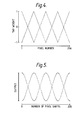
- Fig. 4 illustrates an arrangement which has proved satisfactory, in which the pattern of weighting values is equivalent to two cycles of an ideal moire waveform.
- the resultant output from each of the rings 14 and 16 as a practical charge pattern is shifted round the circle is shown in Fig. 5; in order to determine the position of the charge pattern on the pixel ring, the phase of the output waveform has to be determined relative to the signals stepping it round the ring. It will be evident from Fig.
- the weighting values relating to the rings 14, 16 may be generated using pixels which also function as the tapped shift register, or by separate pixel and register rings.
- the output signal in each position is an analogue function, and it is possible to determine the position of an intersection, and hence the phase of the signal envelope, to a fraction of a pixel dimension.
- the accuracy which can be achieved in this interpolation process is limited by a number of practical factors, of which electrical noise and variations in pixel sensitivity are likely to be the most important; in practice, a sub-division to an eighth of a pixel shift could be considered reasonable.
- Fig. 6 illustrates a representative case of an intersection occuring at a fractional part of a pixel dimension.
- the output signal values represented by the points A, B, C and D are respectively S n-1 ,S n ,S n+1 and ; S n + 2 , as they occur respectively at (n-1), n, (n+l) and (n+2) pixel shifts.
- the effective position of the intersection may be regarded as the intersection of the straight lines AC and BD; for arithmetic convenience it has been shown in the position represented by (n+x/8) pixel shifts where x is an integer, although in practice the fractional portion can take any value between 0 and 1.
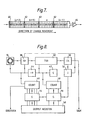
- the signals derived from the charge sensing electrodes of the arrangement shown in Fig. 3) sequentially through its elements at a rate which is a multiple of the rate at which the signals are received.
- the multiple is preferably 2 n +l where n is integral.
- the signals in the register are then modified by weighting values and the result analysed.
- n is set at 3 so signals enter the register at element 60 and are propagated at nine times the rate at which the charge is stepped round the pixel ring on the sensor, so that at all times the signals in the tapped shift register performing the interpolation are spaced nine elements apart.
- the tapped shift register of Fig. 7 is acting as an analogue processor for solving equations; and could be used in situations other than those where the imput signals are position related.
- the block diagram of Fig. 8 illustrates the operation of a tapped shift register interpolation processor in conjunction with one of the pixel rings 14 or 16 of the sensor 10 shown in Fig. 2.
- the output from the sensor 10 is transferred through a sample and hold circuit 38 to the input of the tapped shift register 40.
- the clock drive circuit 42 controls charge transfer within the shift register 40, and the divider circuit 44 generates waveforms at one ninth of the main clock frequency to control charge transfer round the sensor 10 and to operate sample and hold circuit 38.
- Counters 46 and 48 register the number of transfers which have taken place in the sensor 10 and shift register 40 respectively.
- the change of sign detector 50 produces an output when the output of the shift register 40 changes sign, and opens the gates 54 and 56 to transfer the counts in registers 46 and 48 to the output register 58.
- an output from the sample and hold circuit 38 inhibits a spurious change of sign output by means of the gate 52.
- a signal from the least significant bit of counter 46 indicates whether.an odd or even number of pixel shifts has taken place, and another signal from the change of sign detector 50 carries the sign of the output of the shift register 40; together, these establish which of the two types of intersection in the waveform illustrated in Fig. 5 has been detected; this information is used, in a conventional manner, to combine the four intersection positions in the range 0-256 pixels into a single measurement of the phase of the charge pattern in the range 0-128 pixels.
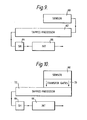
- Fig. 9 represents a simplified block diagram of a sensor and separate processor equivalent to one pixel ring of the sensor in Fig. 2.
- the sensor 60 represents a 256 pixel linear array, or a circular array having an electrical break in the circle such that the signals on the individual pixels emerge sequentially.
- the tapped processor 62 contains 512 elements, having weighting values varying as two repetitions of Fig. 4, namely, four complete cycles of weighting value variation.
- the effect of 256 shifts along the processor is exactly equivalent to shifting the charge pattern on one of the pixel rings of the sensor 10 in Fig. 2 once round the complete circle; with two cycles of a moire pattern on the sensor 60, the output from the processor 62 will be similar to that illustrated in Fig. 5. It will be evident that the output signal from the processor 62 can be transferred through a sample and hold circuit 64 to an interpolation processor 66, corresponding to the sammple and hold circuit 38 and the processor 40 of Fig. 8.
- FIG. 10 An alternative method of transferring signals from a sensor to a processor register is illustrated in Fig. 10, in which signals from the sensor 68 are shifted laterally through a set of transfer gates 709 into the first portion of the tapped processor 72, instead of being transferred serially as in the arrangement of Fig. 9.
- An important advantage of the parallel transfer arrangement of Fig. 10 is that the timing of transfer charge from the sensor 68 may in certain cases be used to control the exposure time of the sensor, which may enable continuous, rather than strobed, illumination to be used. Parallel transfer of sensor signals into the processor would not affect subsequent processing techniques, and the processor 72 could be followed by a sample and hold circuit 64 and an interpolation processor 66 in exactly the same way as the processor 62 of Fig. 9 and the sensor 10 of Fig. 8.
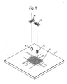
- the master scale 74 carries an orthogonal grid pattern 75 of equispaced straight lines, which it is possible conveniently to produce by photographing diffraction patterns generated by an interferometer; although Fig. 11 shows the grid pattern extending only'over a small area, it will be apparent that its extent requires to be sufficient for the required measuring range.
- the grid pattern 75 of the scale 74 is imaged by lenses 76 and 78 respectively on two linear sensors 80 and 82 having their charge transfer directions ("axes") respectively parallel to the two line directions on the scale 74.
- the lenses 76 and 78 and the sensors 80 and 82 are in a rigid mechanical mounting (not shown) which is free to move in two dimensions in a plane parallel to that of the scale 74; alternatively, the lenses and sensors can remain stationary, and the scale 74 move relatively to them.
- the lenses 76 and 78 are so arranged that the images of the grid pattern 75 generate a moire pattern on the sensors 80 and 82: for example, with 126 line pairs on the grid corresponding to 256 pixels in the sensors 80 and 82.
- the sensors will desirably have the pixel dimension in a direction perpendicular to the axis substantially larger than the width of the pixel along the axis, so that the sensor is sensitive to movement of the scale image along its axis and insensitive to movement of the image perpendicular to the axis.
- the sensors may be mounted with their axes slightly out of parallel with the line direction on the scale 74.
- Fig. 11 constitutes a two-dimensional measuring system, capable of performing precise interpolation between the grid lines 75 on scale 74, while at the same time averaging individual line errors by using a relatively large number of lines in each measurement.
- the integral part of the line count can be derived from the processed outputs of the sensors 80 and 82, or it can be obtained by separate conventional counting means (not shown).
- the sensors could be positioned in the image plane of a single lens, although this might complicate the optical design since either one or both of the sensors would be operating off the axis of the lens.
- both sensors could be formed on the same silicon chip, which would render the off-axis dimension negligible, or they could be arranged to intersect, although the design problems would be daunting.
- each line pair on the grid 75 can be sub-divided into 1024 divisions.
- an interpolation processor capable of determining the phase of the moire pattern to 1/8 of a pixel shift
- each line pair on the grid 75 can be sub-divided into 1024 divisions.
- One way to achieve this would be to vary the lens position automatically to maintain the signal output from the processor at its maximum level, indicating that thp wavelength of the moire'pattern corresponded with that defined by the processor tappings.
- An alternative method of controlling the line spacing in the image relative to the pixel spacing on the sensor is to rotate the sensor slightly about the optic axis.
Landscapes
- Engineering & Computer Science (AREA)
- Theoretical Computer Science (AREA)
- Physics & Mathematics (AREA)
- General Physics & Mathematics (AREA)
- Optical Transform (AREA)
- Length Measuring Devices With Unspecified Measuring Means (AREA)
- Transmission And Conversion Of Sensor Element Output (AREA)
- Length Measuring Devices By Optical Means (AREA)
Applications Claiming Priority (2)
| Application Number | Priority Date | Filing Date | Title |
|---|---|---|---|
| GB8423086 | 1984-09-12 | ||
| GB848423086A GB8423086D0 (en) | 1984-09-12 | 1984-09-12 | Position sensor |
Publications (3)
| Publication Number | Publication Date |
|---|---|
| EP0184286A2 true EP0184286A2 (fr) | 1986-06-11 |
| EP0184286A3 EP0184286A3 (en) | 1988-06-29 |
| EP0184286B1 EP0184286B1 (fr) | 1991-12-11 |
Family
ID=10566640
Family Applications (1)
| Application Number | Title | Priority Date | Filing Date |
|---|---|---|---|
| EP85306354A Expired - Lifetime EP0184286B1 (fr) | 1984-09-12 | 1985-09-06 | Capteur de position |
Country Status (7)
| Country | Link |
|---|---|
| US (1) | US4779211A (fr) |
| EP (1) | EP0184286B1 (fr) |
| JP (1) | JP2546823B2 (fr) |
| CA (1) | CA1262270A (fr) |
| DE (1) | DE3584877D1 (fr) |
| GB (1) | GB8423086D0 (fr) |
| IN (1) | IN166172B (fr) |
Cited By (6)
| Publication number | Priority date | Publication date | Assignee | Title |
|---|---|---|---|---|
| GB2189663A (en) * | 1986-04-24 | 1987-10-28 | Seafarer Navigation Internatio | Direction indicators |
| US5218769A (en) * | 1990-10-19 | 1993-06-15 | Valeo Electronique | Sensor for sensing angle of rotation and/or number of rotations effected, and a power steering system for a vehicle including such a sensor |
| FR2688587A1 (fr) * | 1992-03-13 | 1993-09-17 | Leviedin David | Procede et dispositif optique de mesure de position longitudinale ou angulaire par des rangements a pixel. |
| US5311666A (en) * | 1991-06-21 | 1994-05-17 | University Of Utah Research Foundation | Rotary displacement measuring apparatus |
| GB2369506A (en) * | 2000-07-17 | 2002-05-29 | Tokai Rika Denki Siesakusho Ka | Apparatus for detecting rotational angle |
| GB2369505A (en) * | 2000-07-19 | 2002-05-29 | Tokai Rika Denki Siesakusho Ka | Apparatus for detecting rotational angle |
Families Citing this family (27)
| Publication number | Priority date | Publication date | Assignee | Title |
|---|---|---|---|---|
| GB2188805B (en) * | 1986-03-27 | 1991-01-09 | Duracell Int | Device |
| DE3726260A1 (de) * | 1987-08-07 | 1989-02-16 | Heidenhain Gmbh Dr Johannes | Positionsmesseinrichtung mit mehreren abtaststellen |
| US5258931A (en) * | 1988-07-08 | 1993-11-02 | Parker-Hannifin Corporation | Precision electronic absolute and relative position sensing device and method of using same |
| GB2230666B (en) * | 1989-04-19 | 1993-04-28 | Mitutoyo Corp | Displacement detector |
| US5060394A (en) * | 1989-04-20 | 1991-10-29 | Homestar International Inc. | Measuring apparatus with readout display |
| US5027526A (en) * | 1989-06-02 | 1991-07-02 | Crane R Stephen | Digital linear measuring device |
| US5003171A (en) * | 1990-01-26 | 1991-03-26 | Allied Signal Inc. | Optical encoding arrangement for absolute angle measurements |
| US5254919A (en) * | 1991-03-22 | 1993-10-19 | Eastman Kodak Company | Encoder system using linear array sensor for high resolution |
| US5561606A (en) * | 1991-08-30 | 1996-10-01 | Nikon Corporation | Method for aligning shot areas on a substrate |
| US5502380A (en) * | 1994-04-28 | 1996-03-26 | Rosemount Inc. | Analog weighted binary absolute position encoder including an array of sense resistors each having material responsive to FWX and nonresponsive to flux |
| US6563101B1 (en) * | 2000-01-19 | 2003-05-13 | Barclay J. Tullis | Non-rectilinear sensor arrays for tracking an image |
| DE10200436B4 (de) * | 2002-01-09 | 2015-04-30 | Dr. Johannes Heidenhain Gmbh | Vorrichtung zur sicheren Positionsüberwachung |
| EP1474653B1 (fr) | 2002-02-14 | 2013-01-02 | Faro Technologies Inc. | Machine portable de mesure de coordonnees avec appareil laser a balayage lineaire |
| US7519493B2 (en) | 2002-02-14 | 2009-04-14 | Faro Technologies, Inc. | Portable coordinate measurement machine with integrated line laser scanner |
| US6973734B2 (en) | 2002-02-14 | 2005-12-13 | Faro Technologies, Inc. | Method for providing sensory feedback to the operator of a portable measurement machine |
| US7881896B2 (en) | 2002-02-14 | 2011-02-01 | Faro Technologies, Inc. | Portable coordinate measurement machine with integrated line laser scanner |
| US6957496B2 (en) | 2002-02-14 | 2005-10-25 | Faro Technologies, Inc. | Method for improving measurement accuracy of a portable coordinate measurement machine |
| USRE42082E1 (en) | 2002-02-14 | 2011-02-01 | Faro Technologies, Inc. | Method and apparatus for improving measurement accuracy of a portable coordinate measurement machine |
| US6952882B2 (en) * | 2002-02-14 | 2005-10-11 | Faro Technologies, Inc. | Portable coordinate measurement machine |
| US7246030B2 (en) | 2002-02-14 | 2007-07-17 | Faro Technologies, Inc. | Portable coordinate measurement machine with integrated line laser scanner |
| US6826843B2 (en) * | 2002-11-25 | 2004-12-07 | Radioshack, Corp. | Electronic compass apparatus and method |
| JP4425078B2 (ja) * | 2004-07-12 | 2010-03-03 | 浜松ホトニクス株式会社 | エンコーダ |
| US7535382B2 (en) * | 2006-10-31 | 2009-05-19 | Mitutoyo Corporation | High speed quadrature counter |
| DE102013221143B4 (de) * | 2013-10-17 | 2025-12-04 | Dr. Johannes Heidenhain Gmbh | Positionsmesseinrichtung |
| FR3031588B1 (fr) * | 2015-01-13 | 2018-11-16 | Hutchinson | Capteurs inductifs de deplacement |
| US10451704B2 (en) * | 2016-02-02 | 2019-10-22 | Kenneth Perlin | Tracking apparatus using light through rotating transmissive diffraction patterns, and method |
| US10859363B2 (en) | 2017-09-27 | 2020-12-08 | Stanley Black & Decker, Inc. | Tape rule assembly with linear optical encoder for sensing human-readable graduations of length |
Family Cites Families (24)
| Publication number | Priority date | Publication date | Assignee | Title |
|---|---|---|---|---|
| GB1284641A (en) * | 1970-01-08 | 1972-08-09 | Ferranti Ltd | Improvements relating to measuring apparatus |
| US3982106A (en) * | 1973-05-14 | 1976-09-21 | Contraves Ag | System for measuring the longitudinal or angular displacement of a movable component |
| US3963098A (en) * | 1974-05-07 | 1976-06-15 | Westinghouse Electric Corporation | Position measurement apparatus |
| US4139889A (en) * | 1974-06-07 | 1979-02-13 | Ingels George W | Apparatus for vehicle position indication |
| US4117602A (en) * | 1977-04-04 | 1978-10-03 | The Laitram Corporation | Electromagnetic compass |
| CH637234A5 (de) * | 1979-05-16 | 1983-07-15 | Ssih Equipment Sa | Einrichtung zur stellungsdetektion, insbesondere zur winkelstellungsdetektion, eines markierungstraegers. |
| US4417317A (en) * | 1980-02-04 | 1983-11-22 | Westinghouse Electric Corp. | Adaptive analog processor |
| US4330769A (en) * | 1980-02-07 | 1982-05-18 | Mostek Corporation | Single electrode sense circuit for charge-coupled transversal filters |
| JPS56153212A (en) * | 1980-04-30 | 1981-11-27 | Toshiba Corp | Encoder |
| JPS56159798A (en) * | 1980-05-12 | 1981-12-09 | Tokyo Shibaura Electric Co | Length or angle measuring device |
| US4445110A (en) * | 1980-07-28 | 1984-04-24 | Itek Corporation | Absolute optical encoder system |
| US4360730A (en) * | 1980-10-16 | 1982-11-23 | Itek Corporation | Encoder alignment method and apparatus |
| DE3131276C2 (de) * | 1981-08-07 | 1986-02-13 | Kernforschungsanlage Jülich GmbH, 5170 Jülich | Verfahren zur Verfestigung von radioaktiven Abfällen |
| US4465928A (en) * | 1981-08-17 | 1984-08-14 | Itek Corporation | Optically multiplexed encoder system |
| US4414754A (en) * | 1982-03-04 | 1983-11-15 | The Laitram Corporation | High resolution compass card position decoder |
| US4572952A (en) * | 1982-07-28 | 1986-02-25 | Adrian March Research Ltd. | Position sensor with moire interpolation |
| GB2126444B (en) * | 1982-09-01 | 1986-03-19 | Rosemount Eng Co Ltd | Position measuring apparatus |
| DE3239108A1 (de) * | 1982-10-22 | 1984-04-26 | Dr. Johannes Heidenhain Gmbh, 8225 Traunreut | Positionsmessverfahren und einrichtungen zur durchfuehrung des verfahrens |
| US4621256A (en) * | 1983-07-15 | 1986-11-04 | Lockheed Missiles & Space Company, Inc. | Apparatus for measuring rate of angular displacement |
| US4606008A (en) * | 1983-07-25 | 1986-08-12 | Cain Encoder Company | Angular position detector |
| JPS6059824A (ja) * | 1983-09-12 | 1985-04-06 | Yokogawa Hokushin Electric Corp | エンコ−ダ |
| US4618941A (en) * | 1983-09-19 | 1986-10-21 | Motorola, Inc. | Apparatus and method for generating filtered multilevel data from NRZ data |
| US4616833A (en) * | 1985-03-11 | 1986-10-14 | Wico Corporation | Target shooting game with photoelectric orientation sensing apparatus |
| US4633224A (en) * | 1985-05-06 | 1986-12-30 | Caterpillar Inc. | Absolute and incremental optical encoder |
-
1984
- 1984-09-12 GB GB848423086A patent/GB8423086D0/en active Pending
-
1985
- 1985-09-06 EP EP85306354A patent/EP0184286B1/fr not_active Expired - Lifetime
- 1985-09-06 DE DE8585306354T patent/DE3584877D1/de not_active Expired - Fee Related
- 1985-09-10 US US06/774,488 patent/US4779211A/en not_active Expired - Lifetime
- 1985-09-10 IN IN706/MAS/85A patent/IN166172B/en unknown
- 1985-09-11 CA CA000490464A patent/CA1262270A/fr not_active Expired
- 1985-09-12 JP JP60200692A patent/JP2546823B2/ja not_active Expired - Lifetime
Cited By (10)
| Publication number | Priority date | Publication date | Assignee | Title |
|---|---|---|---|---|
| GB2189663A (en) * | 1986-04-24 | 1987-10-28 | Seafarer Navigation Internatio | Direction indicators |
| US5218769A (en) * | 1990-10-19 | 1993-06-15 | Valeo Electronique | Sensor for sensing angle of rotation and/or number of rotations effected, and a power steering system for a vehicle including such a sensor |
| US5311666A (en) * | 1991-06-21 | 1994-05-17 | University Of Utah Research Foundation | Rotary displacement measuring apparatus |
| FR2688587A1 (fr) * | 1992-03-13 | 1993-09-17 | Leviedin David | Procede et dispositif optique de mesure de position longitudinale ou angulaire par des rangements a pixel. |
| GB2369506A (en) * | 2000-07-17 | 2002-05-29 | Tokai Rika Denki Siesakusho Ka | Apparatus for detecting rotational angle |
| US6555808B2 (en) | 2000-07-17 | 2003-04-29 | Kabushiki Kaisha Tokai Rika Denki Seisakusho | Apparatus for detecting rotational angle |
| GB2369506B (en) * | 2000-07-17 | 2004-09-22 | Tokai Rika Co Ltd | Apparatus for detecting rotational angle |
| GB2369505A (en) * | 2000-07-19 | 2002-05-29 | Tokai Rika Denki Siesakusho Ka | Apparatus for detecting rotational angle |
| US6574876B2 (en) | 2000-07-19 | 2003-06-10 | Kabushiki Kaisha Tokai Rika Denki Seisakusho | Apparatus for detecting rotational angle |
| GB2369505B (en) * | 2000-07-19 | 2004-06-30 | Tokai Rika Denki Siesakusho Ka | Apparatus for detecting rotational angle |
Also Published As
| Publication number | Publication date |
|---|---|
| DE3584877D1 (de) | 1992-01-23 |
| CA1262270A (fr) | 1989-10-10 |
| EP0184286A3 (en) | 1988-06-29 |
| JPS61111417A (ja) | 1986-05-29 |
| EP0184286B1 (fr) | 1991-12-11 |
| JP2546823B2 (ja) | 1996-10-23 |
| IN166172B (fr) | 1990-03-24 |
| US4779211A (en) | 1988-10-18 |
| GB8423086D0 (en) | 1984-10-17 |
Similar Documents
| Publication | Publication Date | Title |
|---|---|---|
| EP0184286B1 (fr) | Capteur de position | |
| US4465373A (en) | Encoder | |
| EP0100243B1 (fr) | Capteur de position | |
| US3982106A (en) | System for measuring the longitudinal or angular displacement of a movable component | |
| EP0042178B1 (fr) | Codeur absolu | |
| US4421980A (en) | Position encoder with closed-ring diode array | |
| EP0765039A2 (fr) | Codeur rotatif | |
| EP0111642B1 (fr) | Méthode et dispositif pour mesurer de déplacement relatif | |
| WO1984001027A1 (fr) | Dispositif de mesure de position | |
| EP1147376B1 (fr) | Capteur de position et circuit pour codeur optique | |
| EP0228721B1 (fr) | Photodétecteur radial semi-conducteur et appareil comportant un tel détecteur | |
| JPS61189415A (ja) | 高精度高分解能絶対位置スケール | |
| JP2537146B2 (ja) | 変位測定装置 | |
| EP0145106B1 (fr) | Lecteur d'un réseau | |
| JPH05196451A (ja) | 測長または測角装置 | |
| WO1991010288A2 (fr) | Detecteur de position | |
| JP2754635B2 (ja) | アブソリュートエンコーダ | |
| JPS636418A (ja) | エンコ−ダ | |
| KR100292806B1 (ko) | 위상 변환 격자를 이용한 엔코더 | |
| RU2220402C2 (ru) | Устройство для измерения положения и перемещения объекта | |
| JPS5853286B2 (ja) | デジタルスケ−ル装置 | |
| JPH05133773A (ja) | 光学式基準位置検出装置 | |
| RU1795706C (ru) | Фотоэлектрический преобразователь положения | |
| JPH09203644A (ja) | 光学式エンコーダ | |
| JPH0481729B2 (fr) |
Legal Events
| Date | Code | Title | Description |
|---|---|---|---|
| PUAI | Public reference made under article 153(3) epc to a published international application that has entered the european phase |
Free format text: ORIGINAL CODE: 0009012 |
|
| AK | Designated contracting states |
Kind code of ref document: A2 Designated state(s): CH DE FR GB IT LI NL SE |
|
| PUAL | Search report despatched |
Free format text: ORIGINAL CODE: 0009013 |
|
| AK | Designated contracting states |
Kind code of ref document: A3 Designated state(s): CH DE FR GB IT LI NL SE |
|
| 17P | Request for examination filed |
Effective date: 19880827 |
|
| 17Q | First examination report despatched |
Effective date: 19900126 |
|
| RAP1 | Party data changed (applicant data changed or rights of an application transferred) |
Owner name: ADRIAN MARCH LIMITED |
|
| GRAA | (expected) grant |
Free format text: ORIGINAL CODE: 0009210 |
|
| AK | Designated contracting states |
Kind code of ref document: B1 Designated state(s): CH DE FR GB IT LI NL SE |
|
| REF | Corresponds to: |
Ref document number: 3584877 Country of ref document: DE Date of ref document: 19920123 |
|
| ITF | It: translation for a ep patent filed | ||
| ET | Fr: translation filed | ||
| PLBE | No opposition filed within time limit |
Free format text: ORIGINAL CODE: 0009261 |
|
| STAA | Information on the status of an ep patent application or granted ep patent |
Free format text: STATUS: NO OPPOSITION FILED WITHIN TIME LIMIT |
|
| 26N | No opposition filed | ||
| EAL | Se: european patent in force in sweden |
Ref document number: 85306354.3 |
|
| PGFP | Annual fee paid to national office [announced via postgrant information from national office to epo] |
Ref country code: FR Payment date: 19990916 Year of fee payment: 15 |
|
| PGFP | Annual fee paid to national office [announced via postgrant information from national office to epo] |
Ref country code: DE Payment date: 19990918 Year of fee payment: 15 |
|
| PGFP | Annual fee paid to national office [announced via postgrant information from national office to epo] |
Ref country code: SE Payment date: 19990920 Year of fee payment: 15 Ref country code: CH Payment date: 19990920 Year of fee payment: 15 |
|
| PGFP | Annual fee paid to national office [announced via postgrant information from national office to epo] |
Ref country code: NL Payment date: 19990921 Year of fee payment: 15 |
|
| PG25 | Lapsed in a contracting state [announced via postgrant information from national office to epo] |
Ref country code: SE Free format text: THE PATENT HAS BEEN ANNULLED BY A DECISION OF A NATIONAL AUTHORITY Effective date: 20000929 |
|
| PG25 | Lapsed in a contracting state [announced via postgrant information from national office to epo] |
Ref country code: LI Free format text: LAPSE BECAUSE OF NON-PAYMENT OF DUE FEES Effective date: 20000930 Ref country code: CH Free format text: LAPSE BECAUSE OF NON-PAYMENT OF DUE FEES Effective date: 20000930 |
|
| PG25 | Lapsed in a contracting state [announced via postgrant information from national office to epo] |
Ref country code: NL Free format text: LAPSE BECAUSE OF NON-PAYMENT OF DUE FEES Effective date: 20010401 |
|
| REG | Reference to a national code |
Ref country code: CH Ref legal event code: PL |
|
| EUG | Se: european patent has lapsed |
Ref document number: 85306354.3 |
|
| PG25 | Lapsed in a contracting state [announced via postgrant information from national office to epo] |
Ref country code: FR Free format text: LAPSE BECAUSE OF NON-PAYMENT OF DUE FEES Effective date: 20010531 |
|
| NLV4 | Nl: lapsed or anulled due to non-payment of the annual fee |
Effective date: 20010401 |
|
| PG25 | Lapsed in a contracting state [announced via postgrant information from national office to epo] |
Ref country code: DE Free format text: LAPSE BECAUSE OF NON-PAYMENT OF DUE FEES Effective date: 20010601 |
|
| REG | Reference to a national code |
Ref country code: FR Ref legal event code: ST |
|
| PGFP | Annual fee paid to national office [announced via postgrant information from national office to epo] |
Ref country code: GB Payment date: 20010823 Year of fee payment: 17 |
|
| REG | Reference to a national code |
Ref country code: GB Ref legal event code: IF02 |
|
| PG25 | Lapsed in a contracting state [announced via postgrant information from national office to epo] |
Ref country code: GB Free format text: LAPSE BECAUSE OF NON-PAYMENT OF DUE FEES Effective date: 20020906 |
|
| GBPC | Gb: european patent ceased through non-payment of renewal fee |
Effective date: 20020906 |