EP0184487A1 - Vorrichtung zum Abscheiden einer Orientierungsschicht für eine Flüssigkristallzelle - Google Patents
Vorrichtung zum Abscheiden einer Orientierungsschicht für eine Flüssigkristallzelle Download PDFInfo
- Publication number
- EP0184487A1 EP0184487A1 EP85402185A EP85402185A EP0184487A1 EP 0184487 A1 EP0184487 A1 EP 0184487A1 EP 85402185 A EP85402185 A EP 85402185A EP 85402185 A EP85402185 A EP 85402185A EP 0184487 A1 EP0184487 A1 EP 0184487A1
- Authority
- EP
- European Patent Office
- Prior art keywords
- source
- liquid crystal
- substrate
- substrates
- orientation
- Prior art date
- Legal status (The legal status is an assumption and is not a legal conclusion. Google has not performed a legal analysis and makes no representation as to the accuracy of the status listed.)
- Granted
Links
- 239000004973 liquid crystal related substance Substances 0.000 title claims abstract description 32
- 238000000151 deposition Methods 0.000 title claims abstract description 25
- 210000002858 crystal cell Anatomy 0.000 title claims abstract description 10
- 239000000758 substrate Substances 0.000 claims abstract description 69
- 230000008021 deposition Effects 0.000 claims abstract description 15
- 238000004544 sputter deposition Methods 0.000 claims abstract description 15
- 239000002245 particle Substances 0.000 claims abstract description 6
- 230000001939 inductive effect Effects 0.000 abstract 1
- 238000001704 evaporation Methods 0.000 description 21
- 230000008020 evaporation Effects 0.000 description 20
- 238000000034 method Methods 0.000 description 18
- PEDCQBHIVMGVHV-UHFFFAOYSA-N Glycerine Chemical compound OCC(O)CO PEDCQBHIVMGVHV-UHFFFAOYSA-N 0.000 description 12
- 230000008569 process Effects 0.000 description 9
- 239000004094 surface-active agent Substances 0.000 description 8
- 210000004027 cell Anatomy 0.000 description 7
- 230000005684 electric field Effects 0.000 description 7
- WSFMFXQNYPNYGG-UHFFFAOYSA-M dimethyl-octadecyl-(3-trimethoxysilylpropyl)azanium;chloride Chemical compound [Cl-].CCCCCCCCCCCCCCCCCC[N+](C)(C)CCC[Si](OC)(OC)OC WSFMFXQNYPNYGG-UHFFFAOYSA-M 0.000 description 5
- 238000004519 manufacturing process Methods 0.000 description 5
- 238000007738 vacuum evaporation Methods 0.000 description 5
- 230000008901 benefit Effects 0.000 description 4
- 210000002421 cell wall Anatomy 0.000 description 3
- 239000007822 coupling agent Substances 0.000 description 3
- 239000011261 inert gas Substances 0.000 description 3
- 239000000463 material Substances 0.000 description 3
- XKRFYHLGVUSROY-UHFFFAOYSA-N Argon Chemical compound [Ar] XKRFYHLGVUSROY-UHFFFAOYSA-N 0.000 description 2
- 239000007864 aqueous solution Substances 0.000 description 2
- 150000002500 ions Chemical class 0.000 description 2
- -1 polytetrafluoroethylene Polymers 0.000 description 2
- 229920001343 polytetrafluoroethylene Polymers 0.000 description 2
- 239000004810 polytetrafluoroethylene Substances 0.000 description 2
- 238000011282 treatment Methods 0.000 description 2
- IIZPXYDJLKNOIY-JXPKJXOSSA-N 1-palmitoyl-2-arachidonoyl-sn-glycero-3-phosphocholine Chemical compound CCCCCCCCCCCCCCCC(=O)OC[C@H](COP([O-])(=O)OCC[N+](C)(C)C)OC(=O)CCC\C=C/C\C=C/C\C=C/C\C=C/CCCCC IIZPXYDJLKNOIY-JXPKJXOSSA-N 0.000 description 1
- XUIMIQQOPSSXEZ-UHFFFAOYSA-N Silicon Chemical group [Si] XUIMIQQOPSSXEZ-UHFFFAOYSA-N 0.000 description 1
- 230000009471 action Effects 0.000 description 1
- 229910052786 argon Inorganic materials 0.000 description 1
- 239000003795 chemical substances by application Substances 0.000 description 1
- VNNRSPGTAMTISX-UHFFFAOYSA-N chromium nickel Chemical compound [Cr].[Ni] VNNRSPGTAMTISX-UHFFFAOYSA-N 0.000 description 1
- 150000001875 compounds Chemical class 0.000 description 1
- 239000004020 conductor Substances 0.000 description 1
- 238000005137 deposition process Methods 0.000 description 1
- 239000012153 distilled water Substances 0.000 description 1
- NBVXSUQYWXRMNV-UHFFFAOYSA-N fluoromethane Chemical class FC NBVXSUQYWXRMNV-UHFFFAOYSA-N 0.000 description 1
- 239000007789 gas Substances 0.000 description 1
- 150000002430 hydrocarbons Chemical class 0.000 description 1
- 239000011810 insulating material Substances 0.000 description 1
- 229940067606 lecithin Drugs 0.000 description 1
- 235000010445 lecithin Nutrition 0.000 description 1
- 239000000787 lecithin Substances 0.000 description 1
- 230000007246 mechanism Effects 0.000 description 1
- 230000007935 neutral effect Effects 0.000 description 1
- 229910001120 nichrome Inorganic materials 0.000 description 1
- 230000003287 optical effect Effects 0.000 description 1
- 150000001282 organosilanes Chemical class 0.000 description 1
- 238000009304 pastoral farming Methods 0.000 description 1
- 229920006122 polyamide resin Polymers 0.000 description 1
- 230000000717 retained effect Effects 0.000 description 1
- 229910052710 silicon Inorganic materials 0.000 description 1
- 238000001179 sorption measurement Methods 0.000 description 1
- 239000007921 spray Substances 0.000 description 1
- 238000012800 visualization Methods 0.000 description 1
- XLYOFNOQVPJJNP-UHFFFAOYSA-N water Chemical compound O XLYOFNOQVPJJNP-UHFFFAOYSA-N 0.000 description 1
Images

Classifications
-
- G—PHYSICS
- G02—OPTICS
- G02F—OPTICAL DEVICES OR ARRANGEMENTS FOR THE CONTROL OF LIGHT BY MODIFICATION OF THE OPTICAL PROPERTIES OF THE MEDIA OF THE ELEMENTS INVOLVED THEREIN; NON-LINEAR OPTICS; FREQUENCY-CHANGING OF LIGHT; OPTICAL LOGIC ELEMENTS; OPTICAL ANALOGUE/DIGITAL CONVERTERS
- G02F1/00—Devices or arrangements for the control of the intensity, colour, phase, polarisation or direction of light arriving from an independent light source, e.g. switching, gating or modulating; Non-linear optics
- G02F1/01—Devices or arrangements for the control of the intensity, colour, phase, polarisation or direction of light arriving from an independent light source, e.g. switching, gating or modulating; Non-linear optics for the control of the intensity, phase, polarisation or colour
- G02F1/13—Devices or arrangements for the control of the intensity, colour, phase, polarisation or direction of light arriving from an independent light source, e.g. switching, gating or modulating; Non-linear optics for the control of the intensity, phase, polarisation or colour based on liquid crystals, e.g. single liquid crystal display cells
- G02F1/133—Constructional arrangements; Operation of liquid crystal cells; Circuit arrangements
- G02F1/1333—Constructional arrangements; Manufacturing methods
- G02F1/1337—Surface-induced orientation of the liquid crystal molecules, e.g. by alignment layers
- G02F1/133734—Surface-induced orientation of the liquid crystal molecules, e.g. by alignment layers by obliquely evaporated films, e.g. Si or SiO2 films
Definitions
- the present invention relates to a device for depositing an orientation layer of a liquid crystal cell.
- Liquid crystal cells are used in particular in display systems for watches, calculators, measuring devices, in peri-computing for the visualization of alphanumeric characters, or even in the optical processing of electrical signals.
- the molecules are generally oriented perpendicular to the cell walls in the absence of an electric field created between the electrodes. Such an orientation is called homeotropic.
- an electric field appears within the liquid crystal. This electric field causes the molecules that orient parallel to the cell walls to tip over. If, before the application of the electric field, the liquid crystal molecules have a homeotropic orientation, under the action of an electric field, they switch indifferently so as to be parallel or anti-parallel to a direction contained in the plane of the cell walls. The appearance of reverse tilt zones, separated from the correct tilt zones by lines of discontinuity, seriously disturbs the appearance of the display.
- a person skilled in the art uses a method which consists in depositing on the substrate surface, by oblique evaporation, a material such as SiO followed by a homeotropic treatment with a surfactant. such as an organic surfactant.
- Figures 1a and 1b schematically represent a device for the implementation of the first step of this known method.
- Figure 1a is a view of the device in a plane parallel to the plane of the substrate 2 such as the xy plane and
- Figure 1b is a view of the same device in a plane perpendicular to the x axis.
- the x and y axes are taken parallel to the sides of the substrate 2 and intersect at its center.
- the source of evaporation comprises a container 4 of elongated and narrow shape, of the order of 40 mm long by 3 mm wide, containing grains 6 of SiO with a diameter of approximately 2 mm and arranged on a single line on the entire length of the container 4. This is placed in the xy 'plane at about 40 cm from the substrate. The angle between the directions y and y' is of the order of a few degrees.
- the source of evaporation also comprises means (not shown) for evaporating the grains 6 of SiO.
- the device finally comprises a shutter 8 which makes it possible to control the duration of exposure of the substrate 2 to the source of evaporation.
- the second step of the process is conventionally the deposition of a surfactant.
- a surfactant Mention may be made, among surface active agents (surfactants), of polyamide resin Versamide 100 and lecithin for hydrocarbon compounds, or polytetrafluoroethylene (PTFE) for fluorocarbon compounds, and among surface coupling agents, organosilanes such as DMOAP polymerized. All of these compounds are known and used by those skilled in the art.
- an orientation layer is deposited by evaporation under vacuum under oblique incidence.
- processes where a layer is deposited under several different angles of evaporation are used, a first layer being deposited under a first angle of evaporation, then a second layer under a second angle of evaporation.
- DE-A-28173 4 8 filed on April 20, 1 978 in the name of CITI-ZEN WATCH Co, Ltd, two coplanar evaporation angles are used simultaneously.
- angles of evaporation are fixed and their values result from a judicious choice by those skilled in the art as a function of numerous parameters.
- orientation layer In addition, vacuum evaporation does not lend itself to mass production of substrates. It is known, in fact, that the orientation layer must have a minimum thickness of the order of 150 mm. It is also known that the thickness of the orientation layer increases all the more rapidly as the direction of evaporation is close to normal to the substrate. However, the deposition of the orientation layer takes place under a significant incidence, the angle between the normal to the substrate and the direction of evaporation being between 60 and 80 °; the thickness of the deposited layer therefore increases slowly.
- the process is further slowed down by the manipulations necessary for positioning each substrate in front of the evaporation source and by the fact that the autonomy of the evaporation source is low, the latter having to be recharged approximately every hour.
- the invention aims to deposit an orientation layer on a substrate to induce a quasi-homeotropic orientation of the molecules of a liquid crystal overcoming the drawbacks of known techniques.
- the invention consists on the one hand in replacing the vacuum evaporation source with a cathode sputtering source and on the other hand in depositing the orientation layer under an incidence varying continuously, the variation interval of l angle of incidence containing the normal incidence.
- cathode sputtering has two essential advantages: first, the source is no longer a point source but extended, which makes it possible to treat large substrates; secondly, the autonomy of this source is much greater than that of a vacuum evaporation source, which limits the stops of the device and accelerates the production rate of the substrates.
- Another advantage is that sputtering allows better control of the material deposited both from the point of view of the amount of the material deposited and its purity.
- the second element of the invention namely the deposition of the orientation layer under a continuously varying incidence, makes it possible to achieve a flow rate compatible with mass production by the movement of a train of substrates under the source of spray.
- the subject of the invention is a device for depositing an orientation layer on the wall of a liquid crystal cell, or substrate, to induce a quasi-homeotropic orientation of the liquid crystal molecules
- a support linear plane capable of receiving a set of substrates aligned along an alignment axis and a sputtering source disposed above said support and centered on said alignment axis, said substrates and said source being driven by a relative movement of translation along said alignment axis during the deposition of the orientation layer, said movement continuously varying the angle of incidence of the particles deposited at each point of a substrate in an interval containing the normal incidence.
- the sputtering source is extended in the plane of the support along an axis perpendicular to the alignment axis.
- the dimension of the source along this axis perpendicular to the alignment axis is at least equal to the dimension of the substrates along this axis.
- the relative translational movement is continuous and at constant speed.
- the sputtering source is stationary and the device comprises a conveyor belt on which the substrates are arranged.
- the substrates are fixed and the sputtering source is driven in a translational movement.
- FIGS. 2a and 2b show a device according to an embodiment of the invention, respectively in front view and in side view.
- This device essentially comprises a source 10 of the body to be deposited, the deposition being carried out by sputtering, and a conveyor belt 12, the upper band of which forms a plane linear support 14 capable of receiving a set of aligned substrates 2.
- the source 10 is arranged opposite the aligned substrates; it is centered on the alignment axis of the substrates.
- Such a device comprises an enclosure filled with an inert gas, for example argon, under a pressure of the order of 0.01 mmHg.
- an inert gas for example argon
- a discharge is created between a cathode, constituted by the source 10 and an anode. This discharge produces the ionization of the neutral gas and the ions formed strike the cathode, causing the molecules to tear from the source. These molecules then have a sufficient speed to reach and deposit on the substrate.
- FIGS. 2a and 2b the source 10 of the body 10 to be deposited on which are precipitated is simply indicated in FIGS. 2a and 2b the inert gas ions. It is clear, however, that the entire device shown in Figures 2a and 2b is contained in an enclosure filled with an inert gas.
- the source 10 is fixed and the substrates pass in front of said source, driven by the motor 16 of the conveyor belt 12.
- This scrolling is preferably done continuously at a constant speed.
- a device comprising a source movable in translation in front of a set of fixed substrates also constitutes an embodiment in accordance with the invention.
- the device of the invention performs the deposition of an orientation layer at an angle of incidence varying continuously during the deposition at each point of the substrate.
- This angle measured between the direction of travel d and the direction of incidence of the particles from the source, varies from an angle ⁇ 1 , less than 90 °, to an angle ⁇ 2 , greater than 90 °.
- the value of the angle 6 can be arbitrary in the interval [0 °, 90 °]; in practice, a value of a few degrees can be retained.
- the value of the angle 6, can be arbitrary in the interval [90 ° .180 °]; in practice a value of almost 180 ° can be used. It is important to note that unlike the known methods, it is not necessary to choose angles here precise incidences, which simplifies the device for depositing the orientation layer (fewer elements, adjustments removed, etc.).
- the deposition according to the invention of an orientation layer under a variable incidence, passing through the normal incidence deviates completely from the known methods in which the angle of incidence is fixed.
- the applicant has deposited an orientation layer on a substrate by means of a device confirmed in FIGS. 2a and 2b and has found, after having deposited a surfactant in a subsequent step, that the liquid crystal molecules deposited on this substrate had a quasi-homeotropic orientation.
- the particles deposited under substantially normal incidence contribute approximately 90% to the thickness of the layer and that the particles deposited under the other incidences contribute only about 10% to the thickness of the layer but are at the origin of the texture of the layer which induces the orientation of the liquid crystal molecules.
- the essential parameters for adjusting the device are the speed of travel of the substrates relative to the source and the power of said source. It is known in fact that the orientation layer must have a minimum thickness, of the order of 150 nm, for the adsorption of the surfactant deposited in the following step to be sufficient. In general, a layer is deposited whose thickness is between 150 and 750 nm.
- the device of the invention has the advantage over known devices, of being suitable for mass production. This is made possible on the one hand by the continuous movement of the substrates in front of the source and, on the other hand, by the use of a sputtering source whose autonomy is much greater than that of a source of evaporation.
- the process for depositing the orientation layer is considerably accelerated in the invention since a large part of the thickness of this layer is deposited under substantially normal incidence, where the growth speed is high, whereas in the processes known, the entire orientation layer is deposited under a substantially grazing fixed incidence, where the growth speed is low.
- the device of the invention makes it possible to treat large substrates.
- the source 10 is a plate, the side of which in the direction of travel, has a length of 10 to 15 cm and the other side of which has a length of 45 cm.
- substrates of about 30 ⁇ 30 cm can be treated, the attitude of the source above the support carrying the substrates being of the order of 5 cm.
- the size of the substrates is limited, in the direction perpendicular to the travel, by the length of the source in this direction.
- the direction of scrolling there is no limitation linked to the device.
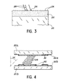
- FIG. 3 a schematic section of a substrate treated with the device of the invention.
- the substrate 20 is covered with an orientation layer 22.
- This orientation layer can be made of an insulating material such as SiO, SiO, AI, O ,. It can also be made of a conductive material such as In, O, or NiCr if it is desired to etch the electrodes in the orientation layer.
- the thickness of this layer is of the order of 150 to 750 nm.
- This layer 22 can be represented as consisting of a superposition of layers, each deposited under a particular incidence, the incidence of deposition of each layer increasing by an angle e, at an angle ⁇ , from the first layer to the last layer deposited.
- the representation of the surface 24 obtained illustrates the orientation of the bodies constituting the surface of the substrate. This representation is of course only a model and does not pretend to be a photograph of reality.
- the second known step of the process for treating a substrate to induce a quasi-homeotropic orientation of liquid crystal molecules consists in covering the surface 24 of this substrate with a surfactant, organic or not, or a coupling agent of area.
- the known process will be described, of depositing a monolecular layer of DMOAP on the substrate.
- the substrate is first immersed in an aqueous solution of DMOAP for 20 minutes.
- This aqueous solution typically contains 0.1% DMOAP.
- the substrate is then rinsed with distilled water for 20 minutes, then dried at room temperature. It is finally heated at 130 ° C for 20 minutes.
- FIG. 3 shows a DMOAP molecule adsorbed on the surface 24.
- the part 26 of this molecule fixed on the surface 24 comprises a tripropyl group linked to a silicon atom.
- Part 28 is composed of an octadecyl carbon chain. It is the orientation of this chain which induces a quasi-homeotropic orientation of the liquid crystal molecules.
- FIG 4 there is shown a schematic section of a liquid crystal cell.
- the substrate 20a forms the upper wall of the cell. On its inner face, are arranged parallel electrodes such as the electrode 30 visible in longitudinal section.
- An orientation layer 22a deposited by means of the device of the invention covers the internal surface of this substrate 20a.
- the other wall of the cell is similarly constituted by a substrate 20b on which are arranged parallel electrodes 32 visible in cross section, the surface of this substrate 20b being covered with an orientation layer 22b obtained deposited at means of the device of the invention.
- a layer of coupling agent (not shown) covers each orientation layer - between these two substrates, liquid crystal molecules 34 are shown having a quasi-homeotropic orientation.
- the angle ⁇ of inclination of these molecules relative to the normal at the walls of the cell has been exaggerated for the clarity of the drawing. In fact, this angle is in practice compns between 1 and 10 °. It is often 1 ° or 2 °.
Landscapes
- Physics & Mathematics (AREA)
- Nonlinear Science (AREA)
- Spectroscopy & Molecular Physics (AREA)
- Mathematical Physics (AREA)
- Chemical & Material Sciences (AREA)
- Crystallography & Structural Chemistry (AREA)
- General Physics & Mathematics (AREA)
- Optics & Photonics (AREA)
- Liquid Crystal (AREA)
- Physical Vapour Deposition (AREA)
Applications Claiming Priority (2)
| Application Number | Priority Date | Filing Date | Title |
|---|---|---|---|
| FR8417794A FR2573548B1 (fr) | 1984-11-22 | 1984-11-22 | Dispositif pour le depot d'une couche d'orientation d'une cellule a cristal liquide |
| FR8417794 | 1984-11-22 |
Publications (2)
| Publication Number | Publication Date |
|---|---|
| EP0184487A1 true EP0184487A1 (de) | 1986-06-11 |
| EP0184487B1 EP0184487B1 (de) | 1989-05-31 |
Family
ID=9309839
Family Applications (1)
| Application Number | Title | Priority Date | Filing Date |
|---|---|---|---|
| EP19850402185 Expired EP0184487B1 (de) | 1984-11-22 | 1985-11-12 | Vorrichtung zum Abscheiden einer Orientierungsschicht für eine Flüssigkristallzelle |
Country Status (4)
| Country | Link |
|---|---|
| EP (1) | EP0184487B1 (de) |
| JP (1) | JPH0792569B2 (de) |
| DE (1) | DE3570771D1 (de) |
| FR (1) | FR2573548B1 (de) |
Cited By (4)
| Publication number | Priority date | Publication date | Assignee | Title |
|---|---|---|---|---|
| EP0286539A1 (de) * | 1987-04-10 | 1988-10-12 | Commissariat A L'energie Atomique | Bistabile smektische ferroelektrische Flüssigkristall-Anzeigevorrichtung |
| WO1989008862A1 (en) * | 1988-03-14 | 1989-09-21 | Hughes Aircraft Company | Light valves with positive dielectric anisotropy liquid crystal and highly tilted off-perpendicular surface alignment, and associated operating method |
| EP0518333A1 (de) * | 1991-06-14 | 1992-12-16 | Hughes Aircraft Company | Verfahren zum vertikalen Ausrichten von Flüssigkristallen |
| FR2725534A1 (fr) * | 1994-10-11 | 1996-04-12 | Luder Ernst | Depot de couches d'orientation sur un substrat pour alignement de molecules de cristaux liquides |
Citations (3)
| Publication number | Priority date | Publication date | Assignee | Title |
|---|---|---|---|---|
| DE2605690A1 (de) * | 1976-01-28 | 1977-08-04 | Bbc Brown Boveri & Cie | Verfahren zum beschichten der innenwaende von fluessigkristallzellen |
| FR2357920A1 (fr) * | 1976-07-06 | 1978-02-03 | Asahi Glass Co Ltd | Element d'affichage a cristal liquide et son procede de fabrication |
| DE2817348A1 (de) * | 1977-04-20 | 1978-10-26 | Citizen Watch Co Ltd | Verfahren und vorrichtung zur bildung einer transparenten duennen orientierungsschicht auf einem substrat einer fluessigkristallzelle |
Family Cites Families (4)
| Publication number | Priority date | Publication date | Assignee | Title |
|---|---|---|---|---|
| JPS5127948A (en) * | 1974-09-02 | 1976-03-09 | Matsushita Electric Industrial Co Ltd | Ekishohyojisochino seizohoho |
| JPS52115244A (en) * | 1976-03-24 | 1977-09-27 | Hitachi Ltd | Orientation control film forming method for liquid crystal display ele ments |
| JPS5699318A (en) * | 1980-01-11 | 1981-08-10 | Citizen Watch Co Ltd | Orientation treatment of liquid crystal cell substrate |
| JPS615232A (ja) * | 1984-03-02 | 1986-01-11 | ビ−ビ−シ− アクチエンゲゼルシヤフト ブラウン ボヴエリ ウント コムパニ− | 配向層の形成方法 |
-
1984
- 1984-11-22 FR FR8417794A patent/FR2573548B1/fr not_active Expired
-
1985
- 1985-11-12 DE DE8585402185T patent/DE3570771D1/de not_active Expired
- 1985-11-12 EP EP19850402185 patent/EP0184487B1/de not_active Expired
- 1985-11-21 JP JP60262346A patent/JPH0792569B2/ja not_active Expired - Lifetime
Patent Citations (3)
| Publication number | Priority date | Publication date | Assignee | Title |
|---|---|---|---|---|
| DE2605690A1 (de) * | 1976-01-28 | 1977-08-04 | Bbc Brown Boveri & Cie | Verfahren zum beschichten der innenwaende von fluessigkristallzellen |
| FR2357920A1 (fr) * | 1976-07-06 | 1978-02-03 | Asahi Glass Co Ltd | Element d'affichage a cristal liquide et son procede de fabrication |
| DE2817348A1 (de) * | 1977-04-20 | 1978-10-26 | Citizen Watch Co Ltd | Verfahren und vorrichtung zur bildung einer transparenten duennen orientierungsschicht auf einem substrat einer fluessigkristallzelle |
Non-Patent Citations (2)
| Title |
|---|
| JAPANESE JOURNAL OF APPLIED PHYSICS, vol. 21, no. 12, partie 2, décembre 1982, pages L761-L763, Tokyo, JP; K. HIROSHIMA: "Controlled high-tilt-angle nematic alignment compatible with glass frit sealing" * |
| PATENTS ABSTRACTS OF JAPAN, vol. 2, no. 1, 5 janvier 1978, page 9551 E 77; & JP - A - 52 115 244 (HITACHI SEISAKUSHO K.K.) 27-09-1977 * |
Cited By (9)
| Publication number | Priority date | Publication date | Assignee | Title |
|---|---|---|---|---|
| EP0286539A1 (de) * | 1987-04-10 | 1988-10-12 | Commissariat A L'energie Atomique | Bistabile smektische ferroelektrische Flüssigkristall-Anzeigevorrichtung |
| FR2613846A1 (fr) * | 1987-04-10 | 1988-10-14 | Commissariat Energie Atomique | Dispositif d'affichage a cristal liquide smectique ferroelectrique bistable |
| US4902106A (en) * | 1987-04-10 | 1990-02-20 | Commissariat A L'energie Atomique | Bistable ferroelectric smectic liquid crystal display device having particular orientation film |
| WO1989008862A1 (en) * | 1988-03-14 | 1989-09-21 | Hughes Aircraft Company | Light valves with positive dielectric anisotropy liquid crystal and highly tilted off-perpendicular surface alignment, and associated operating method |
| EP0518333A1 (de) * | 1991-06-14 | 1992-12-16 | Hughes Aircraft Company | Verfahren zum vertikalen Ausrichten von Flüssigkristallen |
| US5350498A (en) * | 1991-06-14 | 1994-09-27 | Hughes Aircraft Company | Inducing tilted perpendicular alignment in liquid crystals |
| US5620755A (en) * | 1991-06-14 | 1997-04-15 | Jvc - Victor Company Of Japan, Ltd. | Inducing tilted perpendicular alignment in liquid crystals |
| FR2725534A1 (fr) * | 1994-10-11 | 1996-04-12 | Luder Ernst | Depot de couches d'orientation sur un substrat pour alignement de molecules de cristaux liquides |
| NL1001346C2 (nl) * | 1994-10-11 | 1998-08-26 | Lueder Ernst | Werkwijze en inrichting voor het aanbrengen van oriënteringslagen op een substraat voor het richten van moleculen van vloeibare kristallen. |
Also Published As
| Publication number | Publication date |
|---|---|
| JPS61132931A (ja) | 1986-06-20 |
| FR2573548B1 (fr) | 1986-12-26 |
| JPH0792569B2 (ja) | 1995-10-09 |
| EP0184487B1 (de) | 1989-05-31 |
| DE3570771D1 (en) | 1989-07-06 |
| FR2573548A1 (fr) | 1986-05-23 |
Similar Documents
| Publication | Publication Date | Title |
|---|---|---|
| CH629002A5 (en) | Passive electrooptic display cell and method for manufacture thereof | |
| US4153529A (en) | Means and method for inducing uniform parallel alignment of liquid crystal material in a liquid crystal cell | |
| EP0322967B1 (de) | Verfahren zur Metallisierung eines Kieselsäure-, Quartz-, Glas- oder Saphirsubstrates und so erhaltenes Substrat | |
| EP0801419A1 (de) | Herstellungsverfahren von einem dünnen Halbleiterfilm, der elektronische Anordnungen enthält | |
| FR2484463A1 (fr) | Procede et appareil de revetement par pulverisation ionique sans gaz | |
| JPH0624249B2 (ja) | 薄膜太陽電池の製造方法 | |
| FR2509927A1 (fr) | Element a onde elastique de surface | |
| EP0184487B1 (de) | Vorrichtung zum Abscheiden einer Orientierungsschicht für eine Flüssigkristallzelle | |
| EP0707237B1 (de) | Verfahren zur Herstellung von Löchern in Photoresistschichten, Anwendung für die Herstellung von Elektronenquelle mit Mikrospitzenemissionskathoden und flachen Bildschirmen | |
| FR2604298A1 (fr) | Procede de realisation d'une prise de contact electrique sur un substrat en hgcdte de conductivite p et application a la fabrication d'une diode n/p | |
| EP0824603B1 (de) | Vorrichtung zum materialbeschichten grossflächiger substrate | |
| FR2657461A1 (fr) | Procede de fabrication d'un dispositif emetteur d'electrons micro-miniature. | |
| WO2024165363A1 (fr) | Structure integree comprenant une couche ferroelectrique a polarisation selective reportee sur un substrat et procede de fabrication | |
| EP0878565B1 (de) | Verfahren und Vorrichtung zum Ätzen | |
| FR2724269A1 (fr) | Porte-substrat electrostatique | |
| EP0103521A2 (de) | Mit einer Platinoxydlage dünnbeschichtete Substrate, Geräte zu deren Herstellung und Produkte die solche Substrate verwenden | |
| FR2602798A1 (fr) | Procede de depot par pulverisation cathodique d'une couche de materiau sur des substrats et dispositif de mise en oeuvre d'un tel procede | |
| EP4662990A1 (de) | Substratmontierte integrierte struktur mit einer ferroelektrischen schicht mit selektiver umkehrpolarisation in der dicke davon und verfahren zur herstellung davon | |
| FR3139735A1 (fr) | Procédé et dispositif de dépôt de couche mince sur surface courbe | |
| FR3020640B1 (fr) | Procede de fabrication d'un film a la surface d'un substrat et application de ce procede a la fabrication d'un film electriquement conducteur et transparent du visible a l'infrarouge | |
| WO1988006195A1 (fr) | Installation pour la fabrication en continu d'une feuille metallique extra-mince par depot electrolytique | |
| EP1607790A1 (de) | Flüssigkristallanzeige-Vorrichtung, die eine heterogene Ausrichtschicht enthält | |
| EP0110772A1 (de) | Löt- und Dichtungsverfahren zum Zusammensetzen von Aufnehmern | |
| JPS5847685B2 (ja) | エキシヨウノ ブンシハイコウノ タメノソウノ セイセイホウホウオヨビソウチ | |
| FR2771810A1 (fr) | Amelioration de la mesure d'epaisseur en temps reel d'un materiau depose dans une installation de depot par evaporation |
Legal Events
| Date | Code | Title | Description |
|---|---|---|---|
| PUAI | Public reference made under article 153(3) epc to a published international application that has entered the european phase |
Free format text: ORIGINAL CODE: 0009012 |
|
| AK | Designated contracting states |
Kind code of ref document: A1 Designated state(s): CH DE GB IT LI NL |
|
| 17P | Request for examination filed |
Effective date: 19861030 |
|
| RAP1 | Party data changed (applicant data changed or rights of an application transferred) |
Owner name: COMMISSARIAT A L'ENERGIE ATOMIQUE |
|
| 17Q | First examination report despatched |
Effective date: 19880727 |
|
| GRAA | (expected) grant |
Free format text: ORIGINAL CODE: 0009210 |
|
| AK | Designated contracting states |
Kind code of ref document: B1 Designated state(s): CH DE GB IT LI NL |
|
| REF | Corresponds to: |
Ref document number: 3570771 Country of ref document: DE Date of ref document: 19890706 |
|
| ITF | It: translation for a ep patent filed | ||
| GBT | Gb: translation of ep patent filed (gb section 77(6)(a)/1977) | ||
| PLBE | No opposition filed within time limit |
Free format text: ORIGINAL CODE: 0009261 |
|
| STAA | Information on the status of an ep patent application or granted ep patent |
Free format text: STATUS: NO OPPOSITION FILED WITHIN TIME LIMIT |
|
| 26N | No opposition filed | ||
| ITTA | It: last paid annual fee | ||
| REG | Reference to a national code |
Ref country code: GB Ref legal event code: IF02 |
|
| PGFP | Annual fee paid to national office [announced via postgrant information from national office to epo] |
Ref country code: NL Payment date: 20041103 Year of fee payment: 20 |
|
| PGFP | Annual fee paid to national office [announced via postgrant information from national office to epo] |
Ref country code: GB Payment date: 20041110 Year of fee payment: 20 |
|
| PGFP | Annual fee paid to national office [announced via postgrant information from national office to epo] |
Ref country code: CH Payment date: 20041129 Year of fee payment: 20 |
|
| PGFP | Annual fee paid to national office [announced via postgrant information from national office to epo] |
Ref country code: DE Payment date: 20041201 Year of fee payment: 20 |
|
| PG25 | Lapsed in a contracting state [announced via postgrant information from national office to epo] |
Ref country code: GB Free format text: LAPSE BECAUSE OF EXPIRATION OF PROTECTION Effective date: 20051111 |
|
| PG25 | Lapsed in a contracting state [announced via postgrant information from national office to epo] |
Ref country code: NL Free format text: LAPSE BECAUSE OF EXPIRATION OF PROTECTION Effective date: 20051112 |
|
| REG | Reference to a national code |
Ref country code: GB Ref legal event code: PE20 |
|
| REG | Reference to a national code |
Ref country code: CH Ref legal event code: PL |
|
| NLV7 | Nl: ceased due to reaching the maximum lifetime of a patent |
Effective date: 20051112 |