EP0186411A2 - Halbleiteranordnung worin ein Halbleiterchip auf einer Basis befestigt ist - Google Patents
Halbleiteranordnung worin ein Halbleiterchip auf einer Basis befestigt ist Download PDFInfo
- Publication number
- EP0186411A2 EP0186411A2 EP85309170A EP85309170A EP0186411A2 EP 0186411 A2 EP0186411 A2 EP 0186411A2 EP 85309170 A EP85309170 A EP 85309170A EP 85309170 A EP85309170 A EP 85309170A EP 0186411 A2 EP0186411 A2 EP 0186411A2
- Authority
- EP
- European Patent Office
- Prior art keywords
- layer
- metal layer
- solder material
- atomic
- chip
- Prior art date
- Legal status (The legal status is an assumption and is not a legal conclusion. Google has not performed a legal analysis and makes no representation as to the accuracy of the status listed.)
- Granted
Links
Images
Classifications
-
- B—PERFORMING OPERATIONS; TRANSPORTING
- B23—MACHINE TOOLS; METAL-WORKING NOT OTHERWISE PROVIDED FOR
- B23K—SOLDERING OR UNSOLDERING; WELDING; CLADDING OR PLATING BY SOLDERING OR WELDING; CUTTING BY APPLYING HEAT LOCALLY, e.g. FLAME CUTTING; WORKING BY LASER BEAM
- B23K35/00—Rods, electrodes, materials, or media, for use in soldering, welding, or cutting
- B23K35/001—Interlayers, transition pieces for metallurgical bonding of workpieces
-
- B—PERFORMING OPERATIONS; TRANSPORTING
- B23—MACHINE TOOLS; METAL-WORKING NOT OTHERWISE PROVIDED FOR
- B23K—SOLDERING OR UNSOLDERING; WELDING; CLADDING OR PLATING BY SOLDERING OR WELDING; CUTTING BY APPLYING HEAT LOCALLY, e.g. FLAME CUTTING; WORKING BY LASER BEAM
- B23K35/00—Rods, electrodes, materials, or media, for use in soldering, welding, or cutting
- B23K35/22—Rods, electrodes, materials, or media, for use in soldering, welding, or cutting characterised by the composition or nature of the material
- B23K35/24—Selection of soldering or welding materials proper
- B23K35/30—Selection of soldering or welding materials proper with the principal constituent melting at less than 1550°C
- B23K35/302—Cu as the principal constituent
-
- H—ELECTRICITY
- H10—SEMICONDUCTOR DEVICES; ELECTRIC SOLID-STATE DEVICES NOT OTHERWISE PROVIDED FOR
- H10W—GENERIC PACKAGES, INTERCONNECTIONS, CONNECTORS OR OTHER CONSTRUCTIONAL DETAILS OF DEVICES COVERED BY CLASS H10
- H10W70/00—Package substrates; Interposers; Redistribution layers [RDL]
- H10W70/20—Conductive package substrates serving as an interconnection, e.g. metal plates
- H10W70/24—Conductive package substrates serving as an interconnection, e.g. metal plates characterised by materials
-
- H—ELECTRICITY
- H10—SEMICONDUCTOR DEVICES; ELECTRIC SOLID-STATE DEVICES NOT OTHERWISE PROVIDED FOR
- H10W—GENERIC PACKAGES, INTERCONNECTIONS, CONNECTORS OR OTHER CONSTRUCTIONAL DETAILS OF DEVICES COVERED BY CLASS H10
- H10W72/00—Interconnections or connectors in packages
- H10W72/30—Die-attach connectors
-
- B—PERFORMING OPERATIONS; TRANSPORTING
- B23—MACHINE TOOLS; METAL-WORKING NOT OTHERWISE PROVIDED FOR
- B23K—SOLDERING OR UNSOLDERING; WELDING; CLADDING OR PLATING BY SOLDERING OR WELDING; CUTTING BY APPLYING HEAT LOCALLY, e.g. FLAME CUTTING; WORKING BY LASER BEAM
- B23K35/00—Rods, electrodes, materials, or media, for use in soldering, welding, or cutting
- B23K35/001—Interlayers, transition pieces for metallurgical bonding of workpieces
- B23K2035/008—Interlayers, transition pieces for metallurgical bonding of workpieces at least one of the workpieces being of silicium
-
- H—ELECTRICITY
- H10—SEMICONDUCTOR DEVICES; ELECTRIC SOLID-STATE DEVICES NOT OTHERWISE PROVIDED FOR
- H10W—GENERIC PACKAGES, INTERCONNECTIONS, CONNECTORS OR OTHER CONSTRUCTIONAL DETAILS OF DEVICES COVERED BY CLASS H10
- H10W72/00—Interconnections or connectors in packages
- H10W72/01—Manufacture or treatment
- H10W72/013—Manufacture or treatment of die-attach connectors
- H10W72/01331—Manufacture or treatment of die-attach connectors using blanket deposition
-
- H—ELECTRICITY
- H10—SEMICONDUCTOR DEVICES; ELECTRIC SOLID-STATE DEVICES NOT OTHERWISE PROVIDED FOR
- H10W—GENERIC PACKAGES, INTERCONNECTIONS, CONNECTORS OR OTHER CONSTRUCTIONAL DETAILS OF DEVICES COVERED BY CLASS H10
- H10W72/00—Interconnections or connectors in packages
- H10W72/071—Connecting or disconnecting
- H10W72/073—Connecting or disconnecting of die-attach connectors
-
- H—ELECTRICITY
- H10—SEMICONDUCTOR DEVICES; ELECTRIC SOLID-STATE DEVICES NOT OTHERWISE PROVIDED FOR
- H10W—GENERIC PACKAGES, INTERCONNECTIONS, CONNECTORS OR OTHER CONSTRUCTIONAL DETAILS OF DEVICES COVERED BY CLASS H10
- H10W72/00—Interconnections or connectors in packages
- H10W72/071—Connecting or disconnecting
- H10W72/073—Connecting or disconnecting of die-attach connectors
- H10W72/07331—Connecting techniques
- H10W72/07336—Soldering or alloying
-
- H—ELECTRICITY
- H10—SEMICONDUCTOR DEVICES; ELECTRIC SOLID-STATE DEVICES NOT OTHERWISE PROVIDED FOR
- H10W—GENERIC PACKAGES, INTERCONNECTIONS, CONNECTORS OR OTHER CONSTRUCTIONAL DETAILS OF DEVICES COVERED BY CLASS H10
- H10W72/00—Interconnections or connectors in packages
- H10W72/30—Die-attach connectors
- H10W72/351—Materials of die-attach connectors
- H10W72/352—Materials of die-attach connectors comprising metals or metalloids, e.g. solders
-
- H—ELECTRICITY
- H10—SEMICONDUCTOR DEVICES; ELECTRIC SOLID-STATE DEVICES NOT OTHERWISE PROVIDED FOR
- H10W—GENERIC PACKAGES, INTERCONNECTIONS, CONNECTORS OR OTHER CONSTRUCTIONAL DETAILS OF DEVICES COVERED BY CLASS H10
- H10W72/00—Interconnections or connectors in packages
- H10W72/50—Bond wires
- H10W72/541—Dispositions of bond wires
- H10W72/5449—Dispositions of bond wires not being orthogonal to a side surface of the chip, e.g. fan-out arrangements
-
- H—ELECTRICITY
- H10—SEMICONDUCTOR DEVICES; ELECTRIC SOLID-STATE DEVICES NOT OTHERWISE PROVIDED FOR
- H10W—GENERIC PACKAGES, INTERCONNECTIONS, CONNECTORS OR OTHER CONSTRUCTIONAL DETAILS OF DEVICES COVERED BY CLASS H10
- H10W72/00—Interconnections or connectors in packages
- H10W72/851—Dispositions of multiple connectors or interconnections
- H10W72/874—On different surfaces
- H10W72/884—Die-attach connectors and bond wires
-
- H—ELECTRICITY
- H10—SEMICONDUCTOR DEVICES; ELECTRIC SOLID-STATE DEVICES NOT OTHERWISE PROVIDED FOR
- H10W—GENERIC PACKAGES, INTERCONNECTIONS, CONNECTORS OR OTHER CONSTRUCTIONAL DETAILS OF DEVICES COVERED BY CLASS H10
- H10W90/00—Package configurations
- H10W90/701—Package configurations characterised by the relative positions of pads or connectors relative to package parts
- H10W90/731—Package configurations characterised by the relative positions of pads or connectors relative to package parts of die-attach connectors
- H10W90/736—Package configurations characterised by the relative positions of pads or connectors relative to package parts of die-attach connectors between a chip and a stacked lead frame, conducting package substrate or heat sink
-
- H—ELECTRICITY
- H10—SEMICONDUCTOR DEVICES; ELECTRIC SOLID-STATE DEVICES NOT OTHERWISE PROVIDED FOR
- H10W—GENERIC PACKAGES, INTERCONNECTIONS, CONNECTORS OR OTHER CONSTRUCTIONAL DETAILS OF DEVICES COVERED BY CLASS H10
- H10W90/00—Package configurations
- H10W90/701—Package configurations characterised by the relative positions of pads or connectors relative to package parts
- H10W90/751—Package configurations characterised by the relative positions of pads or connectors relative to package parts of bond wires
- H10W90/756—Package configurations characterised by the relative positions of pads or connectors relative to package parts of bond wires between a chip and a stacked lead frame, conducting package substrate or heat sink
Definitions
- the present invention relates to a semiconductor device and, more particularly, to an improvement in the bonding layer when a semiconductor chip is fixed to a base such as a lead frame.
- this structure has the following drawbacks.
- the Ni layer reacts with silicon (Si) contained in the chip, and nickel silicide is easily formed.
- the V layer is interposed between the Ni layer and Si of the element chip, the bottom surface of the element chip is not flat and is normally roughened on the order of several microns so as to improve a bonding property with respect to the bonding layer.
- the thicknesa of the V layer varies, and when heated, Ni is easily diffused to the bottom surface of the element chip.
- the nickel silicide itself is fragile, and undergoes a considerable volume variation due to a change in density during its formation process.
- the semiconductor device when used, e.g., in an atmosphere of high humidity, a local cell is formed between the Ni layer and the Au-Ge alloy layer, and as a result, electrical characteristics of the semiconductor device may be degraded or the chip may be displaced from the base.
- the solder material comprises gold as its major component, it is expensive and increases the cost of the semiconductor device.
- a semiconductor device in which a semiconductor chip is fixed to a base such as a lead frame through a bonding layer, wherein poor contact or peeling of the bonding layer does not easily occur, cost of the bonding layer can be decreased, and the electrical characteristics of the semiconductor element will not be adversely influenced by the bonding layer.
- a semiconductor device in which a semiconductor chip is fixed to a base by a solder material layer consisting of a tin-copper alloy, wherein a first metal layer consisting of a metal selected from the group consisting of titanium, chromium, vanadium, zirconium and niobium or an alloy containing not less than 75 atomic % of at least one of the metals and having a thickness falling within the range between 2,000 A and 3 ⁇ m is interposed between the solder material layer and the semiconductor chip.
- a semiconductor device wherein a second metal layer consisting of a metal selected from the group consisting of nickel and cobalt or an alloy containing not less than 75 atomic % of at least one of the metals and having a thickness smaller than that of the first metal layer is interposed between the first metal layer and the solder material layer.
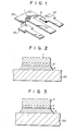
- Fig. 1 shows a state wherein a semiconductor chip, e.g., is bonded to a lead frame.
- reference numeral 1 denotes a semiconductor chip; and 2a, 2b and 2c; lead frames.
- the chip 1 is connected to the lead frames 2b and 2c through bonding wires 3.
- a first metal layer 4 is deposited on the back surface of the chip 1, and a solder material layer 5 is deposited thereon.
- the chip 1 is disposed on and'fixed to the lead frame 2a through the layer 5.
- a metal selected from the group consisting of titanium (Ti), chromium (Cr), vanadium (V), zirconium (Zr) and niobium (Nb) or an alloy containing 75 atomic % or more of at least one of these metals is used.
- the thickness of the layer 4 is 0 0 set to be 2,000 A to 3 ⁇ m and preferably 2,300 A to 1 ⁇ m. When the thickness of the layer 4 is below 0 2,000 A, the preventive effect of Cu diffusion in the solder material may become insufficient. Although there is no problem if the thickness of the layer 4 is set to be larger than 3 ⁇ m, it is undesirable in view of manufacturing time and cost.
- the metal layer 4 is not limited to a single layer as shown in Fig. 2, but can be a multilayer in which two or more metal layers consisting of two or more metals selected from the group consisting of Ti, Cr, V, Zr and Nb are stacked. This also applies when an alloy of these metals is used. When two or more layers are stacked, a total thickness of the layer 4 preferably 0 falls within the range between 2,000 A and 3 ⁇ m.
- preferable metals to be interposed as a barrier layer (the first metal layer) between the layer 5 and the chip 1 are Ti, Cr and V. This is because Zr and Nb require a deposition temperature of 2,400°C or higher and do not allow easy control of deposition conditions.
- phosphorus (P) or boron (B) can be added to the layer 4 so as to further improve the barrier effect.
- the solder material layer 5 preferably consists of a tin-copper (Sn-Cu) alloy, and more preferably contains 13.3 to 75 atomic %, preferably 30 to 75 atomic %, most preferably 50 to 65 atomic % of Cu.
- Sn and Cu forming the layer 5 have substantially the same melting point (for example, Sn: 1,685 K, Cu: 1,690 K at 0.1 Torr).
- a deposited Sn-Cu alloy composition can be the same as the deposition source composition, the Sn-Cu alloy is melted at relatively low temperatures (e.g., in the case of Sn(38 to 92.4 wt%)-Cu, the melting point is 415°C), and the Sn-Cu alloy is inexpensive as compared to an Au-Ge alloy.
- the layer 5 can contain 53 atomic % or less of zinc (Zn) based upon the content of copper, or can contain 25 atomic % or less of aluminum (Al ) based thereupon. When Zn or Al is added, thermal and electrical conductivity coefficients are increased, and electrical characteristics and reliability of the semiconductor device can be improved.
- the thickness of the layer 5 is normally set to be 1 ⁇ m to 3 ⁇ m.
- a gold (Au) layer having a thickness of 1,500 to 3,000 ⁇ can be formed on the surface of the layer 5 so as to prevent oxidation.
- Fig. 3 shows a modification of a semiconductor device according to the present invention.
- a sole difference between this modification and the embodiment shown in Fig. 2 is that a second metal layer 6 as a thermal shock absorbing layer is interposed between the first metal layer 4 and the solder material layer 6.
- the second metal layer 6 a metal selected from the group consisting of nickel and cobalt or an alloy containing 75 atomic % or more of at least one of these metals is used.
- the layer 6 has a thermal expansion coefficient between those of the layers 4 and 5 so as to absorb internal strain upon application of a thermal shock.
- the thickness of the layer 6 is preferably set to be smaller than that of the layer 4.
- a high thermal shock resistance can be obtained by decreasing the thickness of the layer 6 below that of the Ni layer in the conventional structure comprising a V layer, an Ni layer and an Sn-Cu alloy layer due to the following facts.
- Ni and Cu form an alloy of all proportional solid solution type, and during soldering, Cu is diffused in Ni, and in an extreme case, pores are formed in Sn-Cu layer 5, thus degrading the mechanical strength.
- the diffusion amount of Cu can be decreased.
- an npn small-signal transistor is used as the semiconductor element chip 1.
- a 3,000 A thick V layer as the first metal layer 4 was deposited on the back surface of a chip 1, and a 1.5 ⁇ m thick Sn-Cu alloy layer (Cu: 50 atomic %) was deposited thereon.
- a 2,600 ⁇ thick V layer as the layer 4 and a 2.1 ⁇ m thick Sn-Cu alloy layer (Cu: 50 atomic %) were sequentially deposited on the back surface of another chip 1. Then, each resultant structure was disposed on a lead frame 2a which was heated to 415°C in advance, and was biased thereagainst, thereby melting the Sn-Cu alloy (the layer 5).
- V CE (sat.) sufficiently falls within an allowable range of 130 mV to 220 mV, and approximately overlaps a target value of 130 mV to 150 mV.
- V BCF achieves a targer value of 1.1 V.
- an adequate value cannot be obtained, and the device cannot be applied in practice.
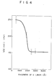
- Example 2 only the thickness of the V layer was varied, and V CE (sat.) was measured. The results are shown in Fig. 4. As can be seen from Fig. 4, it was confirmed that appropriate V CE (sat.) can be obtained when the thickness of the V layer is set to be 2,000 A or more. Note that in these Examples, when a V-Co (5 wt%) alloy layer was used in place of the V layer, the same effect could be obtained.
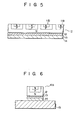
- a V layer 12, a Ti layer 13 and an Sn-Cu (40 atom.%) layer 14 were sequentially deposited on a bottom surface of an Si substrate 11 on which a plurality of npn transistors 11a, 11b,... were formed.
- the V layer 12 had a thickness of 690 ⁇
- the Ti layer 13 had a thickness of 2,700 ⁇
- the Sn-Cu layer 14 had a thickness of 1.5 ⁇ m.
- a 2,000 ⁇ thick Au layer as an antioxidant layer was deposited on the surface of the Sn-Cu layer 14. Thereafter, the resultant structure was cut into transistor chips by a diamond scribe technique.
- the transistor chip was attached to a Cu lead frame 15 at a temperature of 450°C, as shown in Fig. 6.
- the Sn-Cu layer 14 was melted by heating and biasing force and was solidified after cooling, thus fixing the chip to the lead frame 15.
- Example 3 In place of the Ti layer of Example 3, a 2,500 ⁇ thick Cr layer was formed. Sn-Cu (44 atom.%) was used as a solder material. The transistor chip was bonded to the lead frame under the same conditions as in Example 3.
- solder material is inexpensive and yield can be improved, this results in a considerable reduction in cost of a semiconductor device.
- Examples 5 and 6 correspond to the embodiment shown in Fig. 3.
- a 2,700 ⁇ thick V layer as the first metal layer 4 a 1,500 ⁇ thick Ni layer as the second metal layer 6 and a 2 ⁇ m thick Sn-Cu alloy solder material layer 5 (Cu: 60 atom.%) were sequentially deposited on the back surface of an npn small-signal transistor (as the semiconductor chip 1), and the resultant structure was bonded to a lead frame 2a.
- Example 6 a 3,000 ⁇ thick Ti layer as the first metal layer 4, a 1,500 ⁇ thick Ni layer as the second metal layer 6 and a 1.5 ⁇ m thick Sn-Cu alloy solder material layer 5 (Cu: 60 atom.%) were sequentially deposited on the back surface of an npn small-signal transistor, and the resultant structure was bonded to another lead frame 2a.
- a 1,000 ⁇ thick V layer and a 2 ⁇ m thick Sn-Cu solder material layer (Cu: 60 atom.%) were sequentially stacked on the back surface of another npn small-signal transistor of the same type and the resultant structure was bonded to a lead frame (Comparative Example 3).
- a 1,000 A thick Ti layer and a 1.5 ⁇ m thick Sn-Cu solder material layer (Cu: 60 atom.%) were sequentially stacked on the back surface of another small-signal transistor of the same type and the resultant structure was bonded to a lead frame (Comparative Example 4).
- TST thermal shock test
- FDT frame dry ice test
- solder resistance test was conducted by examining the adhesion state of the solder to the wafer as follows.
- the silicon wafer on which first and second metal layers 4 and 6 and the solder material layer 5 were deposited was first dipped in a Pb-Sn eutectic solder (230°C) to pick up a portion of the Pb-Sn entectic solder on the surface of the layer 5.
- a Pb-Sn eutectic solder 230°C
- the wafer was split into two.
- an adhesion strength between the Sn-Cu and the silicon wafer was regarded sufficient, and the wafer was evaluated as a good wafer.
- the adhesion strength was regarded insufficient and such a wafer was evaluated as a defective wafer.
- a semiconductor device which has excellent electrical characteristics and high reliability can be obtained by Sn-Cu soldering.
Landscapes
- Engineering & Computer Science (AREA)
- Mechanical Engineering (AREA)
- Die Bonding (AREA)
Applications Claiming Priority (6)
| Application Number | Priority Date | Filing Date | Title |
|---|---|---|---|
| JP59276075A JPS61156823A (ja) | 1984-12-28 | 1984-12-28 | 半導体装置 |
| JP276077/84 | 1984-12-28 | ||
| JP276104/84 | 1984-12-28 | ||
| JP59276104A JPS61156825A (ja) | 1984-12-28 | 1984-12-28 | 半導体装置 |
| JP59276077A JPS61156824A (ja) | 1984-12-28 | 1984-12-28 | 半導体装置 |
| JP276075/84 | 1984-12-28 |
Publications (3)
| Publication Number | Publication Date |
|---|---|
| EP0186411A2 true EP0186411A2 (de) | 1986-07-02 |
| EP0186411A3 EP0186411A3 (en) | 1987-04-01 |
| EP0186411B1 EP0186411B1 (de) | 1991-02-27 |
Family
ID=27336314
Family Applications (1)
| Application Number | Title | Priority Date | Filing Date |
|---|---|---|---|
| EP85309170A Expired - Lifetime EP0186411B1 (de) | 1984-12-28 | 1985-12-16 | Halbleiteranordnung worin ein Halbleiterchip auf einer Basis befestigt ist |
Country Status (5)
| Country | Link |
|---|---|
| US (1) | US4954870A (de) |
| EP (1) | EP0186411B1 (de) |
| KR (1) | KR900008971B1 (de) |
| CN (1) | CN85109419B (de) |
| DE (1) | DE3581905D1 (de) |
Cited By (4)
| Publication number | Priority date | Publication date | Assignee | Title |
|---|---|---|---|---|
| EP0585084A1 (de) * | 1992-08-28 | 1994-03-02 | AT&T Corp. | Verfahren für eine permanente metallische Verbindung |
| WO1996026808A1 (de) * | 1995-03-01 | 1996-09-06 | Fraunhofer-Gesellschaft zur Förderung der angewandten Forschung e.V. | Untermetallisierung für lotmaterialien |
| EP0833384A3 (de) * | 1996-09-25 | 1999-10-13 | Siemens Aktiengesellschaft | Halbleiterkörper mit Lotmaterialschicht |
| US6220501B1 (en) * | 1997-10-13 | 2001-04-24 | Kabushiki Kaisha Toshiba | Method of joining metallic members, and joined metallic members |
Families Citing this family (18)
| Publication number | Priority date | Publication date | Assignee | Title |
|---|---|---|---|---|
| US4954870A (en) * | 1984-12-28 | 1990-09-04 | Kabushiki Kaisha Toshiba | Semiconductor device |
| JPH0555575A (ja) * | 1991-08-29 | 1993-03-05 | Sharp Corp | 半導体装置 |
| JP2796919B2 (ja) * | 1992-05-11 | 1998-09-10 | インターナショナル・ビジネス・マシーンズ・コーポレーション | メタライゼーション複合体および半導体デバイス |
| US5454929A (en) * | 1994-06-16 | 1995-10-03 | National Semiconductor Corporation | Process for preparing solderable integrated circuit lead frames by plating with tin and palladium |
| US5503286A (en) * | 1994-06-28 | 1996-04-02 | International Business Machines Corporation | Electroplated solder terminal |
| DE19527209A1 (de) * | 1995-07-27 | 1997-01-30 | Philips Patentverwaltung | Halbleitervorrichtung |
| AU2002318144A1 (en) * | 2001-05-24 | 2003-01-29 | Fry's Metals, Inc. | Thermal interface material and heat sink configuration |
| EP1695382A4 (de) * | 2001-05-24 | 2007-10-10 | Fry Metals Inc | Thermisches grenzflächenmaterial und lot-preforms |
| JP4882229B2 (ja) * | 2004-09-08 | 2012-02-22 | 株式会社デンソー | 半導体装置およびその製造方法 |
| JP2006100739A (ja) * | 2004-09-30 | 2006-04-13 | Toshiba Corp | 接合体、半導体装置、接合方法及び半導体装置の製造方法 |
| DE102005061263B4 (de) * | 2005-12-20 | 2007-10-11 | Infineon Technologies Austria Ag | Halbleiterwafersubstrat für Leistungshalbleiterbauelemente sowie Verfahren zur Herstellung desselben |
| US8502257B2 (en) * | 2009-11-05 | 2013-08-06 | Visera Technologies Company Limited | Light-emitting diode package |
| KR101067190B1 (ko) * | 2010-02-03 | 2011-09-22 | 삼성전기주식회사 | 파워 패키지 모듈 및 그 제조방법 |
| US8836120B2 (en) | 2011-04-19 | 2014-09-16 | Infineon Technologies Ag | Semiconductor device with a layer including niobium, and/or tantalum overlying a contact pad or a metal layer |
| JP2015056646A (ja) * | 2013-09-13 | 2015-03-23 | 株式会社東芝 | 半導体装置及び半導体モジュール |
| CN109704269A (zh) * | 2017-10-25 | 2019-05-03 | 中芯国际集成电路制造(上海)有限公司 | 一种mems器件及制备方法、电子装置 |
| CN110238504B (zh) * | 2019-07-04 | 2021-06-08 | 中国航空制造技术研究院 | 一种钛-钢合金高强度扩散连接方法 |
| KR102698553B1 (ko) * | 2023-12-05 | 2024-08-23 | 주식회사 하늘바이오 농업회사법인 | 인삼 부각의 제조방법 |
Family Cites Families (12)
| Publication number | Priority date | Publication date | Assignee | Title |
|---|---|---|---|---|
| CA859342A (en) * | 1970-12-22 | Csakvary Tibor | Hard solder electrical device | |
| DE1639366B2 (de) * | 1968-01-26 | 1975-10-02 | Konstantin Andrejewitsch Preobraschenzey | Verfahren zur Herstellung eines Kontaktes für Halbleiterbauelemente |
| BE763522A (fr) * | 1970-03-03 | 1971-07-16 | Licentia Gmbh | Serie de couches de contact pour des elements de construction semi-conducteurs |
| US3679492A (en) * | 1970-03-23 | 1972-07-25 | Ibm | Process for making mosfet's |
| DE2514922C2 (de) * | 1975-04-05 | 1983-01-27 | SEMIKRON Gesellschaft für Gleichrichterbau u. Elektronik mbH, 8500 Nürnberg | Gegen thermische Wechselbelastung beständiges Halbleiterbauelement |
| JPS5575226A (en) * | 1978-12-04 | 1980-06-06 | Toshiba Corp | Manufacturing semiconductor device |
| WO1982002457A1 (en) * | 1980-12-30 | 1982-07-22 | Finn John B | Die attachment exhibiting enhanced quality and reliability |
| JPS586143A (ja) * | 1981-07-02 | 1983-01-13 | Matsushita Electronics Corp | 半導体装置 |
| DE3312713A1 (de) * | 1983-04-08 | 1984-10-11 | The Furukawa Electric Co., Ltd., Tokio/Tokyo | Silberbeschichtete elektrische materialien und verfahren zu ihrer herstellung |
| JPS59193036A (ja) * | 1983-04-16 | 1984-11-01 | Toshiba Corp | 半導体装置の製造方法 |
| US4954870A (en) * | 1984-12-28 | 1990-09-04 | Kabushiki Kaisha Toshiba | Semiconductor device |
| JPH05432A (ja) * | 1991-06-24 | 1993-01-08 | Seiko Instr Inc | 射出成形用金型 |
-
1985
- 1985-12-05 US US06/804,617 patent/US4954870A/en not_active Expired - Fee Related
- 1985-12-16 EP EP85309170A patent/EP0186411B1/de not_active Expired - Lifetime
- 1985-12-16 DE DE8585309170T patent/DE3581905D1/de not_active Expired - Lifetime
- 1985-12-18 KR KR1019850009521A patent/KR900008971B1/ko not_active Expired
- 1985-12-27 CN CN85109419A patent/CN85109419B/zh not_active Expired
Cited By (5)
| Publication number | Priority date | Publication date | Assignee | Title |
|---|---|---|---|---|
| EP0585084A1 (de) * | 1992-08-28 | 1994-03-02 | AT&T Corp. | Verfahren für eine permanente metallische Verbindung |
| WO1996026808A1 (de) * | 1995-03-01 | 1996-09-06 | Fraunhofer-Gesellschaft zur Förderung der angewandten Forschung e.V. | Untermetallisierung für lotmaterialien |
| EP0833384A3 (de) * | 1996-09-25 | 1999-10-13 | Siemens Aktiengesellschaft | Halbleiterkörper mit Lotmaterialschicht |
| US6268659B1 (en) | 1996-09-25 | 2001-07-31 | Infineon Technologies Ag | Semiconductor body with layer of solder material comprising chromium |
| US6220501B1 (en) * | 1997-10-13 | 2001-04-24 | Kabushiki Kaisha Toshiba | Method of joining metallic members, and joined metallic members |
Also Published As
| Publication number | Publication date |
|---|---|
| KR900008971B1 (ko) | 1990-12-15 |
| DE3581905D1 (de) | 1991-04-04 |
| EP0186411B1 (de) | 1991-02-27 |
| KR860005438A (ko) | 1986-07-23 |
| US4954870A (en) | 1990-09-04 |
| CN85109419A (zh) | 1986-06-10 |
| EP0186411A3 (en) | 1987-04-01 |
| CN85109419B (zh) | 1988-06-08 |
Similar Documents
| Publication | Publication Date | Title |
|---|---|---|
| EP0186411B1 (de) | Halbleiteranordnung worin ein Halbleiterchip auf einer Basis befestigt ist | |
| US6187114B1 (en) | Solder material and electronic part using the same | |
| CA2155091C (en) | Bonding material and bonding method for electric element | |
| US5217922A (en) | Method for forming a silicide layer and barrier layer on a semiconductor device rear surface | |
| KR100286151B1 (ko) | 집적 회로 패키지, 리드 프레임, 및 그 제조물 | |
| EP1939938B1 (de) | Halbleiterbauelement und Herstellungsverfahren und Kupferleitungen | |
| US5234149A (en) | Debondable metallic bonding method | |
| US8763884B2 (en) | Joint with first and second members with a joining layer located therebetween containing Sn metal and another metallic material; methods for forming the same joint | |
| JP3372548B2 (ja) | 半田接合用表面処理構造体及びそれを用いた無フラックス半田付方法 | |
| JP2007152385A (ja) | 高温半田及び高温半田ペースト材、及びそれを用いたパワー半導体装置 | |
| EP0585084A1 (de) | Verfahren für eine permanente metallische Verbindung | |
| EP0823731A2 (de) | Verfahren zum Erzeugen eines Halbleitermetallisierungssystems und Struktur dafür | |
| JPH07221217A (ja) | 半導体パッケージ用リッドおよび半導体パッケージ | |
| EP2800129A1 (de) | Verbindungsstruktur | |
| JPWO1994014190A1 (ja) | 半田接合用表面処理構造体及びそれを用いた無フラックス半田付方法 | |
| US5622305A (en) | Bonding scheme using group VB metallic layer | |
| USH498H (en) | Electronic component including soldered electrical leads | |
| GB2138633A (en) | Bonding semiconductor chips to a lead frame | |
| EP0880801A1 (de) | BEFESTIGTER SiC-WÜRFEL UND VERFAHREN ZUR BEFESTIGUNG VON SiC-WÜRFELN | |
| JPH05175252A (ja) | 半導体電極構造体 | |
| GB2300375A (en) | Bonding method for electric element | |
| US3115694A (en) | Method of producing a silicon semiconductor device | |
| TW202603098A (zh) | 導電性接著膜、異種材料之接合方法、半導體元件結構體,及切割黏晶膜 | |
| JPH11347785A (ja) | 半導体ダイボンディング用半田とそのテープ及び半導体装置 | |
| TW202547964A (zh) | 導電性接著膜、異種材料之接合方法、半導體元件結構體,及切割黏晶膜 |
Legal Events
| Date | Code | Title | Description |
|---|---|---|---|
| PUAI | Public reference made under article 153(3) epc to a published international application that has entered the european phase |
Free format text: ORIGINAL CODE: 0009012 |
|
| AK | Designated contracting states |
Kind code of ref document: A2 Designated state(s): DE FR GB |
|
| 17P | Request for examination filed |
Effective date: 19861002 |
|
| PUAL | Search report despatched |
Free format text: ORIGINAL CODE: 0009013 |
|
| AK | Designated contracting states |
Kind code of ref document: A3 Designated state(s): DE FR GB |
|
| 17Q | First examination report despatched |
Effective date: 19890908 |
|
| GRAA | (expected) grant |
Free format text: ORIGINAL CODE: 0009210 |
|
| AK | Designated contracting states |
Kind code of ref document: B1 Designated state(s): DE FR GB |
|
| REF | Corresponds to: |
Ref document number: 3581905 Country of ref document: DE Date of ref document: 19910404 |
|
| ET | Fr: translation filed | ||
| PLBE | No opposition filed within time limit |
Free format text: ORIGINAL CODE: 0009261 |
|
| STAA | Information on the status of an ep patent application or granted ep patent |
Free format text: STATUS: NO OPPOSITION FILED WITHIN TIME LIMIT |
|
| 26N | No opposition filed | ||
| PGFP | Annual fee paid to national office [announced via postgrant information from national office to epo] |
Ref country code: GB Payment date: 19971208 Year of fee payment: 13 |
|
| PGFP | Annual fee paid to national office [announced via postgrant information from national office to epo] |
Ref country code: FR Payment date: 19971209 Year of fee payment: 13 |
|
| PG25 | Lapsed in a contracting state [announced via postgrant information from national office to epo] |
Ref country code: GB Free format text: LAPSE BECAUSE OF NON-PAYMENT OF DUE FEES Effective date: 19981216 |
|
| GBPC | Gb: european patent ceased through non-payment of renewal fee |
Effective date: 19981216 |
|
| PG25 | Lapsed in a contracting state [announced via postgrant information from national office to epo] |
Ref country code: FR Free format text: LAPSE BECAUSE OF NON-PAYMENT OF DUE FEES Effective date: 19990831 |
|
| REG | Reference to a national code |
Ref country code: FR Ref legal event code: ST |
|
| PGFP | Annual fee paid to national office [announced via postgrant information from national office to epo] |
Ref country code: DE Payment date: 20041209 Year of fee payment: 20 |