EP0186460A2 - Photodétecteur à semi-conducteurs - Google Patents
Photodétecteur à semi-conducteurs Download PDFInfo
- Publication number
- EP0186460A2 EP0186460A2 EP85309306A EP85309306A EP0186460A2 EP 0186460 A2 EP0186460 A2 EP 0186460A2 EP 85309306 A EP85309306 A EP 85309306A EP 85309306 A EP85309306 A EP 85309306A EP 0186460 A2 EP0186460 A2 EP 0186460A2
- Authority
- EP
- European Patent Office
- Prior art keywords
- layer
- inp
- gainas
- gainasp
- type
- Prior art date
- Legal status (The legal status is an assumption and is not a legal conclusion. Google has not performed a legal analysis and makes no representation as to the accuracy of the status listed.)
- Granted
Links
Images

Classifications
-
- H—ELECTRICITY
- H10—SEMICONDUCTOR DEVICES; ELECTRIC SOLID-STATE DEVICES NOT OTHERWISE PROVIDED FOR
- H10F—INORGANIC SEMICONDUCTOR DEVICES SENSITIVE TO INFRARED RADIATION, LIGHT, ELECTROMAGNETIC RADIATION OF SHORTER WAVELENGTH OR CORPUSCULAR RADIATION
- H10F77/00—Constructional details of devices covered by this subclass
- H10F77/10—Semiconductor bodies
- H10F77/12—Active materials
- H10F77/124—Active materials comprising only Group III-V materials, e.g. GaAs
- H10F77/1248—Active materials comprising only Group III-V materials, e.g. GaAs having three or more elements, e.g. GaAlAs, InGaAs or InGaAsP
-
- H—ELECTRICITY
- H10—SEMICONDUCTOR DEVICES; ELECTRIC SOLID-STATE DEVICES NOT OTHERWISE PROVIDED FOR
- H10F—INORGANIC SEMICONDUCTOR DEVICES SENSITIVE TO INFRARED RADIATION, LIGHT, ELECTROMAGNETIC RADIATION OF SHORTER WAVELENGTH OR CORPUSCULAR RADIATION
- H10F30/00—Individual radiation-sensitive semiconductor devices in which radiation controls the flow of current through the devices, e.g. photodetectors
- H10F30/20—Individual radiation-sensitive semiconductor devices in which radiation controls the flow of current through the devices, e.g. photodetectors the devices having potential barriers, e.g. phototransistors
- H10F30/21—Individual radiation-sensitive semiconductor devices in which radiation controls the flow of current through the devices, e.g. photodetectors the devices having potential barriers, e.g. phototransistors the devices being sensitive to infrared, visible or ultraviolet radiation
- H10F30/22—Individual radiation-sensitive semiconductor devices in which radiation controls the flow of current through the devices, e.g. photodetectors the devices having potential barriers, e.g. phototransistors the devices being sensitive to infrared, visible or ultraviolet radiation the devices having only one potential barrier, e.g. photodiodes
- H10F30/223—Individual radiation-sensitive semiconductor devices in which radiation controls the flow of current through the devices, e.g. photodetectors the devices having potential barriers, e.g. phototransistors the devices being sensitive to infrared, visible or ultraviolet radiation the devices having only one potential barrier, e.g. photodiodes the potential barrier being a PIN barrier
-
- H—ELECTRICITY
- H10—SEMICONDUCTOR DEVICES; ELECTRIC SOLID-STATE DEVICES NOT OTHERWISE PROVIDED FOR
- H10F—INORGANIC SEMICONDUCTOR DEVICES SENSITIVE TO INFRARED RADIATION, LIGHT, ELECTROMAGNETIC RADIATION OF SHORTER WAVELENGTH OR CORPUSCULAR RADIATION
- H10F30/00—Individual radiation-sensitive semiconductor devices in which radiation controls the flow of current through the devices, e.g. photodetectors
- H10F30/20—Individual radiation-sensitive semiconductor devices in which radiation controls the flow of current through the devices, e.g. photodetectors the devices having potential barriers, e.g. phototransistors
- H10F30/21—Individual radiation-sensitive semiconductor devices in which radiation controls the flow of current through the devices, e.g. photodetectors the devices having potential barriers, e.g. phototransistors the devices being sensitive to infrared, visible or ultraviolet radiation
- H10F30/22—Individual radiation-sensitive semiconductor devices in which radiation controls the flow of current through the devices, e.g. photodetectors the devices having potential barriers, e.g. phototransistors the devices being sensitive to infrared, visible or ultraviolet radiation the devices having only one potential barrier, e.g. photodiodes
- H10F30/225—Individual radiation-sensitive semiconductor devices in which radiation controls the flow of current through the devices, e.g. photodetectors the devices having potential barriers, e.g. phototransistors the devices being sensitive to infrared, visible or ultraviolet radiation the devices having only one potential barrier, e.g. photodiodes the potential barrier working in avalanche mode, e.g. avalanche photodiodes
-
- Y—GENERAL TAGGING OF NEW TECHNOLOGICAL DEVELOPMENTS; GENERAL TAGGING OF CROSS-SECTIONAL TECHNOLOGIES SPANNING OVER SEVERAL SECTIONS OF THE IPC; TECHNICAL SUBJECTS COVERED BY FORMER USPC CROSS-REFERENCE ART COLLECTIONS [XRACs] AND DIGESTS
- Y02—TECHNOLOGIES OR APPLICATIONS FOR MITIGATION OR ADAPTATION AGAINST CLIMATE CHANGE
- Y02E—REDUCTION OF GREENHOUSE GAS [GHG] EMISSIONS, RELATED TO ENERGY GENERATION, TRANSMISSION OR DISTRIBUTION
- Y02E10/00—Energy generation through renewable energy sources
- Y02E10/50—Photovoltaic [PV] energy
- Y02E10/544—Solar cells from Group III-V materials
-
- Y—GENERAL TAGGING OF NEW TECHNOLOGICAL DEVELOPMENTS; GENERAL TAGGING OF CROSS-SECTIONAL TECHNOLOGIES SPANNING OVER SEVERAL SECTIONS OF THE IPC; TECHNICAL SUBJECTS COVERED BY FORMER USPC CROSS-REFERENCE ART COLLECTIONS [XRACs] AND DIGESTS
- Y10—TECHNICAL SUBJECTS COVERED BY FORMER USPC
- Y10S—TECHNICAL SUBJECTS COVERED BY FORMER USPC CROSS-REFERENCE ART COLLECTIONS [XRACs] AND DIGESTS
- Y10S148/00—Metal treatment
- Y10S148/015—Capping layer
-
- Y—GENERAL TAGGING OF NEW TECHNOLOGICAL DEVELOPMENTS; GENERAL TAGGING OF CROSS-SECTIONAL TECHNOLOGIES SPANNING OVER SEVERAL SECTIONS OF THE IPC; TECHNICAL SUBJECTS COVERED BY FORMER USPC CROSS-REFERENCE ART COLLECTIONS [XRACs] AND DIGESTS
- Y10—TECHNICAL SUBJECTS COVERED BY FORMER USPC
- Y10S—TECHNICAL SUBJECTS COVERED BY FORMER USPC CROSS-REFERENCE ART COLLECTIONS [XRACs] AND DIGESTS
- Y10S148/00—Metal treatment
- Y10S148/072—Heterojunctions
-
- Y—GENERAL TAGGING OF NEW TECHNOLOGICAL DEVELOPMENTS; GENERAL TAGGING OF CROSS-SECTIONAL TECHNOLOGIES SPANNING OVER SEVERAL SECTIONS OF THE IPC; TECHNICAL SUBJECTS COVERED BY FORMER USPC CROSS-REFERENCE ART COLLECTIONS [XRACs] AND DIGESTS
- Y10—TECHNICAL SUBJECTS COVERED BY FORMER USPC
- Y10S—TECHNICAL SUBJECTS COVERED BY FORMER USPC CROSS-REFERENCE ART COLLECTIONS [XRACs] AND DIGESTS
- Y10S148/00—Metal treatment
- Y10S148/097—Lattice strain and defects
-
- Y—GENERAL TAGGING OF NEW TECHNOLOGICAL DEVELOPMENTS; GENERAL TAGGING OF CROSS-SECTIONAL TECHNOLOGIES SPANNING OVER SEVERAL SECTIONS OF THE IPC; TECHNICAL SUBJECTS COVERED BY FORMER USPC CROSS-REFERENCE ART COLLECTIONS [XRACs] AND DIGESTS
- Y10—TECHNICAL SUBJECTS COVERED BY FORMER USPC
- Y10S—TECHNICAL SUBJECTS COVERED BY FORMER USPC CROSS-REFERENCE ART COLLECTIONS [XRACs] AND DIGESTS
- Y10S148/00—Metal treatment
- Y10S148/12—Photocathodes-Cs coated and solar cell
Definitions
- The'present invention relates to semiconductor photodetectors, such as a PIN photodiode and an avalanche photodiode.
- Photodetectors for optical fiber communication systems in the 1.3 to 1.6 ⁇ m wavelength region include PIN photodiodes and avalanche photodiodes made of a III-V alloy system, e.g., GaInAs/InP system.
- a photodiode comprises an InP substrate, an InP buffer layer, an GaInAs light absorbing layer, and an InP cap layer, these layers being epitaxially formed in succession on the InP substrate. Heterojunctions are formed at interfaces between the InP buffer layer and GaInAs layer, and between the GaInAs layer and InP cap layer.
- a PIN photodiode is produced, for example, in the following manner. First, an undoped (N - -type) InP buffer layer is epitaxially grown on a (100) oriented N + -type InP substrate; an undoped (N -type) GaInAs light absorbing layer is epitaxially grown on the InP buffer layer; and an N-type InP cap layer is also epitaxially grown on the GaInAs layer.
- a P-type region is formed as a light receiving area in the InP cap layer by a thermal diffusion process; an antireflecting film is formed on the P-type region; and a protecting film is formed on the InP cap layer.
- a P-side electrode and an N-side electrode are formed on the P +- type region and the InP substrate, respectively.
- the growing conditions are controlled so that the lattice constant of the grown layers matches that of the InP substrate, to decrease the possibility of lattice mismatching. It is easy to match the lattice constant of InP layer to that of the InP substrate, since the InP layer and the InP substrate can have the same composition, but when the GaInAs layer is epitaxially grown on the InP layer, i.e. InP substrate, it is necessary to control the composition ratio of Ga to In in the GaInAs layer so that the lattice constant of the GaInAs matches that of the InP.
- the thermal expansion coefficient of GaInAs is 1.24 times larger than that of InP; i.e. the thermal expansion coefficient of InP is 4.56 x 10- 6 K -1 and that of GaInAs is 5.66 x 10 K . Therefore, when the GaInAs layer is grown at a temperature of, typically, from 600°C to 700°C to obtain a lattice match with the InP layer, the shrinkage of the GaInAs layer is more than that of the InP layer, at a room temperature, with the result that strain is generated, which causes mismatching between the layers. In another method, it is possible to grow the GaInAs layer in a mismatching condition so that the GaInAs and InP will match when cooled at room temperature.
- a semiconductor photodetector comprising an InP substrate, a first InP layer, a GaInAs (or GaInAsP) layer, and a second InP layer, which layers are successively epitaxially formed by a vapor phase epitaxial process on said InP substrate, a lattice constant of said GaInAs (or GaInAsP) layer being larger than that of said first InP layer at room temperature.
- a semiconductor photodetector comprising an InP substrate, a first InP layer, a GaInAsP layer, and a second InP layer, which layers are successively epitaxially formed by a vapor phase epitaxial process on said InP substrate, a lattice constant of said GaInAsP layer being larger than that of said first InP layer at room temperature.
- a semiconductor photodetector comprising an InP substrate, a first InP layer, a GaInAs layer, a GaInAsP layer, and a second InP layer, which layers are successively epitaxially formed by a vapor phase epitaxial process on said InP substrate, a lattice constant of said GaInAs layer being larger than that of said first InP layer at room temperature and a lattice constant of said GaInAsP layer lying in the range between said InP layer lattice constant and said GaInAs layer lattice constant, inclusively.
- PIN photodiodes are produced at the same time by performing the vapor-phase epitaxial growth of the GaInAs layer under the above-mentioned preferable condition, the properties of the produced PIN photodiodes are not satisfactory, in particular, a problem of dark current in the photodiodes occurs frequently.
- An embodiment of the present invention may provide an improved photodetector made of a III-IV alloy system, such as GaInAn/InP, and GaInAsP/InP. provid An embodiment of the present invention may vide a photodetector, such as a PIN photodiode and an avalanche photodiode, having a GaInAs/InP or GaInAsP/InP system, with a low dark current.
- a photodetector such as a PIN photodiode and an avalanche photodiode, having a GaInAs/InP or GaInAsP/InP system, with a low dark current.
- the present invention is based on the discovery of the inventors that at the lattice mismatching degree Aa/a between the GaInAs (or GaInAsP) light absorbing layer and the InP buffer layer in the positive (plus) range (especially, from 0 to 0.2%) the dark current is lower than the negative (minus) range (outside the range of 0 to 0.2%) at room temperature.
- the GaInAs (or GaInAsP) light absorbing layer having an energy bandgap smaller than the InP layer, being a dark current generating region, is under a tension stress at minus Aa/a, but is under a compression stress at plus Aa/a.
- the present inventors have assumed that the crystal state of the GaInAs (or GaInAsP) layer under a compression stress is more stable than that under a tension stress.
- the lattice constance of the GaInAs (or GaInAsP) layer is larger than that of the first InP layer at room temperature. All of the layers are sequentially grown by a vapor phase epitaxial process.
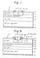
- a PIN photodiode comprises, for example, an N + -type InP substrate 1, an undoped N -type InP buffer layer 2, an undoped N -type GaInAs (or GaInAsP) light absorbing layer 3, an N-type InP cap layer 4, and a passivation film 5.
- a P -type region 6 is formed in the InP cap layer 4 and extends into the GaInAs (or GaInAsP) layer 3.
- An antireflecting 1 film 7 is formed on the P + -type region 6, a P-side electrode 8 is formed on a portion of the P + -type region 6, and an N-side electrode 9 is formed on the InP substrate 1.
- the above structure is that of a PIN photodiode. to which the present invention may be applied,
- a PIN photodiode/illustrated in Fig. 1, may be produced / for example as follows.
- a (100) oriented N +- type InP wafer having an impurity concentration of approximately 4 x 10 18 cm -3 is prepared as the substrate 1.
- the InP buffer layer 2 having a thickness of 3 ⁇ m and an impurity concentration of approximately 5 x 10 14 cm -3 is grown by a vapor phase epitaxial process, under the following conditions.
- a carrier gas of H 2 is made to flow through PC1 3 liquid to feed an H2 + PCl 3 gas at a flow rate of 300 cm /min into a reactor.
- an In source and the InP substrate 1 are heated at 800°C and 670°C, respectively.
- An additional carrier gas of H 2 is fed into the reactor, so that the total H 2 flow rate at the growth region is 956 cm 3 /min.
- the InP layer 2 is grown at a growth rate 0 of approximately 12 A/sec.
- the GaInAs layer 3 having a thickness of 1.6 ⁇ m and an impurity concentration of approximately 1 x 10 15 cm -3 is grown on the InP layer 2 by vapor phase epitaxy under the following conditions.
- a carrier gas of H 2 is made to flow through AsCl 3 liquid to feed an H 2 + AsCl 3 gas into the reactor.
- a portion of the H 2 + AsCl 3 gas is made to flow at a flow rate of 144 cm 3 /min over a Ga source heated at 750°C and the rest of the H 2 + AsCl 3 gas to flow at a flow rate of 312 cm 3 /min over another In source heated at 800°C.
- An additional carrier gas of H 2 is fed into the reactor, so that the total H 2 flow rate at the growth region in which the substrate 1 is heated at 67 0 °C is 956 cm 3 /min.
- the Ga 0.45 In 0.55 As layer 3 is grown at a growth rate of approximately 3 A/sec.
- an atomic ratio "x" of In to Ga in Ga 1-x In x As can be varied by controlling a ratio of the flow rate of the H 2 + AsCl 3 gas over the In source to that of the H 2 + AsCl 3 gas over the Ga source. Therefore, the lattice constance of the GaInAs layer can be varied, so that a lattice mismatching degree Aa/a also can be varied.
- the InP cap layer 4 having a thickness of 1 ⁇ m and an impurity concentration of approximately 1 x 10 cm is grown in a similar manner to that of the InP buffer layer 2,'except that donor impurities (sulfur) are doped.
- the passivation film 5 of silicon nitride and having a thickness of approximately 0.18 um is formed on the InP cap layer 4 by a plasma chemical vapor deposition (CVD).
- the silicon nitride film 5 is then selectively etched by conventional photo-lithography to form an opening for a photodetective region.
- the P +- type region 6 is formed by thermally diffusing zinc (Zn) into the InP cap layer 4 through the opening of the silicon nitride film 5 at 500°C.
- the diffused Zn reaches a portion of the GaInAs layer 3, so that the bottom of the P +- type region 7 is in the GaInAs layer 3, as shown in Fig. 1.
- the surface impurity concentration of the P + -type region 7 is approximately 4 x 10 18 cm -3 .
- the antireflection film 7 of silicon nitride having a thickness of 1.8 ⁇ m is formed on the exposed surface of the P + -type region 6 by plasma CVD.
- silicon nitride is also deposited on the formed silicon nitride film 5, so that the thickness of the passivation film 5 of silicon nitride is increased.
- the antireflection film 7 is selectively etched by conventional photo-lithography to form an opening for may be the electrode 8.
- the diameter d of a photodetective for example. may be region is 80 ⁇ m /
- the GaInAs layer is vapor phase epitaxially grown under the condition that the lattice constant of the grown GaInAs layer is larger than that of the InP layer at the growing temperature.
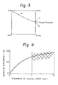
- a lattice matching condition for InP in a GalnAsPquaternary system is indicated with a dot and dash line A, including Ga 0.47 In 0.53 As in a GaInAs ternary system.
- a GaInAs having a composition at a point B is grown due to Aa/a ⁇ 0, an embodiment of whereas in/the present invention a GaInAs having a composition at a point C is grown under the limitation of 0 ⁇ ⁇ a/a ⁇ 0.2.
- the thickness of the GaInAs layer As to the thickness of the GaInAs layer, a thicker GaInAs layer having +Aa/a applies a stronger fcrce on the heterojunction interface. Accordingly, it is preferable that the GaInAs layer be thin. However, too thin a GaInAs layer brings about a decrease of the quantum efficiency of the layer.
- Figure 4 shows a relationship between the GaInAs layer thickness and the quantum efficiency; the abscissa showing the thickness of a GaInAs layer and the ordinate showing the corresponding quantum efficiency.
- the quantum efficiency n at 1.3 ⁇ m is calculated by the following formula:
- an avalanche photodiode to/ comprises, for example, a (100) N + -type InP substrate 21, an N-type InP layer 22, an undoped N - -type GaInAs light absorbing layer 23, an undoped N -type GaInAsP thin layer 24, an N-type InP layer 25, and an N -type InP layer 26.
- a passivation film 27 is formed on the N -type InP layer 26
- a P + -type region 28 is formed in the N -type InP layer 26
- an antireflection film 29 is formed on the P + -type region 28.
- a P-side electrode 30 and an N-side electrode 31 are formed on a portion of the P + -type region 28 and on the InP substrate 21, respectively.
- the lattice constant of the GaInAs layer 23 is larger than that of the InP layer 22 at room temperature.
- the lattice constant of the GaInAsP layer lies in the range between the InP lattice constant and the GaInAs layer lattice constant, inclusively, at room temperature.
- another undoped N -type GaInAsP thin layer (not shown) be formed between the N-type InP layer 22 and the GaInAsP layer 23.
- the GaInAsP layer has an energy bandgap Eg having an intermediate value (0.9 eV) between that of InP (1.35 eV) and GaInAs (0.75 eV).
- the GaInAsP layer has intermediate energy bandgap and lattice constant values, and thus can improve the frequency property of an avalanche photodiode.
- An avalanche photodiode illustrated in Fig. 5/ may be produced, for example, in the following manner.
- a (100) oriented N +- type InP wafer having an impurity concentration of approximately 4 x 10 18 cm -3 is prepared as the substrate 21.
- layers 22 to 26 having the thicknesses and impurity concentrations shown in Table 1 are successively grown by a vapor phase epitaxial process mentioned hereinbefore.
- the growing conditions are controlled so as to make the lattice constant of GaInAs larger than that of InP at room temperature.
- the growing conditions for the GaInAsP layer 24 are controlled so as to make the lattice constant of GaInAsP not less than that of InP and not more than that of the formed GaInAs layer at room temperature.
- the passivation film 27 of silicon nitride with an opening is formed by a plasma CVD process and by conventional photo-lithography.
- Zn is introduced into the N - -type InP layer 26 by a thermal diffusion process to form the P + -type region 28 having a surface impurity con- centration of 4 x 10 18 cm
- the antireflection film 29 of silicon nitride having a thickness of 0.18 ⁇ m is formed on the P + -type region 28 by the plasma CVD process.
- the electrode 30 of AuZn and the electrode 31 of AuGe are formed on the P +- type region 28 and the InP substrate 21, respectively, as shown in Fig. 5.
- a light receiving area has a diameter d of 80 ⁇ m for exampel. Thus a low dark current avalanche photodiode embodying the present invention is obtained.
Landscapes
- Light Receiving Elements (AREA)
- Junction Field-Effect Transistors (AREA)
Applications Claiming Priority (2)
| Application Number | Priority Date | Filing Date | Title |
|---|---|---|---|
| JP269652/84 | 1984-12-22 | ||
| JP59269652A JPS61172381A (ja) | 1984-12-22 | 1984-12-22 | InP系化合物半導体装置 |
Publications (3)
| Publication Number | Publication Date |
|---|---|
| EP0186460A2 true EP0186460A2 (fr) | 1986-07-02 |
| EP0186460A3 EP0186460A3 (en) | 1986-12-10 |
| EP0186460B1 EP0186460B1 (fr) | 1991-05-29 |
Family
ID=17475331
Family Applications (1)
| Application Number | Title | Priority Date | Filing Date |
|---|---|---|---|
| EP85309306A Expired - Lifetime EP0186460B1 (fr) | 1984-12-22 | 1985-12-20 | Photodétecteur à semi-conducteurs |
Country Status (5)
| Country | Link |
|---|---|
| US (1) | US4906583A (fr) |
| EP (1) | EP0186460B1 (fr) |
| JP (1) | JPS61172381A (fr) |
| KR (1) | KR890004963B1 (fr) |
| DE (1) | DE3583010D1 (fr) |
Cited By (10)
| Publication number | Priority date | Publication date | Assignee | Title |
|---|---|---|---|---|
| EP0279651A1 (fr) * | 1987-02-17 | 1988-08-24 | Bt&D Technologies Limited | Fabrication d'une couche de couverture |
| EP0308335A3 (en) * | 1987-09-16 | 1989-12-06 | Sumitomo Electric Industries Limited | Ingaas/inp type pin photodiodes |
| EP0296428A3 (en) * | 1987-06-19 | 1990-05-23 | International Business Machines Corporation | Heterojunction interdigitated schottky barrier photodetector |
| AU602143B2 (en) * | 1986-04-30 | 1990-10-04 | Sumitomo Electric Industries, Ltd. | Compound semiconductor device |
| US5040039A (en) * | 1990-01-25 | 1991-08-13 | Mitsubishi Denki Kabushiki Kaisha | Semiconductor photodetector device |
| US5047832A (en) * | 1989-03-10 | 1991-09-10 | Sumitomo Electric Industries, Ltd. | Electrode structure for III-V compound semiconductor element and method of manufacturing the same |
| US5115294A (en) * | 1989-06-29 | 1992-05-19 | At&T Bell Laboratories | Optoelectronic integrated circuit |
| EP0522746A1 (fr) * | 1991-07-01 | 1993-01-13 | Mitsubishi Denki Kabushiki Kaisha | Dispositif photodétecteur semi-conducteur |
| EP0538878A3 (en) * | 1991-10-25 | 1993-08-04 | Sumitomo Electric Industries, Ltd. | Light detecting device |
| EP0557955A1 (fr) * | 1992-02-24 | 1993-09-01 | Sumitomo Electric Industries, Limited | Photodétecteur |
Families Citing this family (26)
| Publication number | Priority date | Publication date | Assignee | Title |
|---|---|---|---|---|
| JP2970815B2 (ja) * | 1990-04-11 | 1999-11-02 | 株式会社東芝 | 半導体受光素子 |
| JPH07123170B2 (ja) * | 1990-08-07 | 1995-12-25 | 光計測技術開発株式会社 | 受光素子 |
| GB9118338D0 (en) * | 1991-08-27 | 1991-10-16 | Secretary Trade Ind Brit | A radiation detector for detecting infrared radiation |
| JP3288741B2 (ja) * | 1992-02-07 | 2002-06-04 | 住友電気工業株式会社 | 半導体受光素子の製造方法 |
| US5391896A (en) * | 1992-09-02 | 1995-02-21 | Midwest Research Institute | Monolithic multi-color light emission/detection device |
| JP2910696B2 (ja) * | 1996-09-20 | 1999-06-23 | 日本電気株式会社 | 半導体光検出器 |
| US6262465B1 (en) * | 1998-09-25 | 2001-07-17 | Picometrix, Inc. | Highly-doped P-type contact for high-speed, front-side illuminated photodiode |
| US6326649B1 (en) * | 1999-01-13 | 2001-12-04 | Agere Systems, Inc. | Pin photodiode having a wide bandwidth |
| AU2996400A (en) * | 1999-03-01 | 2000-09-21 | Sensors Unlimited Inc. | Doped structures for improved ingaas performance in imaging devices |
| CA2307745A1 (fr) * | 1999-07-15 | 2001-01-15 | Sumitomo Electric Industries, Ltd. | Photodiode |
| KR100366046B1 (ko) * | 2000-06-29 | 2002-12-27 | 삼성전자 주식회사 | 에벌란치 포토다이오드 제조방법 |
| JP2002050785A (ja) * | 2000-08-01 | 2002-02-15 | Sumitomo Electric Ind Ltd | 半導体受光素子 |
| EP1198015A3 (fr) * | 2000-09-13 | 2004-04-14 | TriQuint Technology Holding Co | Dispositif optoélectronique dopé pour augmenter le seuil de puissance optique pour l'effondrement de largeur de bande et méthode de fabrication |
| US6627501B2 (en) * | 2001-05-25 | 2003-09-30 | Macronix International Co., Ltd. | Method of forming tunnel oxide layer |
| US6518080B2 (en) * | 2001-06-19 | 2003-02-11 | Sensors Unlimited, Inc. | Method of fabricating low dark current photodiode arrays |
| JP2003264309A (ja) * | 2002-03-08 | 2003-09-19 | Toshiba Corp | 光半導体装置および光半導体装置の製造方法 |
| JP2006080448A (ja) * | 2004-09-13 | 2006-03-23 | Sumitomo Electric Ind Ltd | エピタキシャルウェハおよび素子 |
| KR101321280B1 (ko) * | 2004-12-07 | 2013-10-25 | 피코메트릭스 엘엘씨 | 광도전 장치 |
| JP4956944B2 (ja) * | 2005-09-12 | 2012-06-20 | 三菱電機株式会社 | アバランシェフォトダイオード |
| JP5015494B2 (ja) * | 2006-05-22 | 2012-08-29 | 住友電工デバイス・イノベーション株式会社 | 半導体受光素子 |
| US20100093127A1 (en) * | 2006-12-27 | 2010-04-15 | Emcore Solar Power, Inc. | Inverted Metamorphic Multijunction Solar Cell Mounted on Metallized Flexible Film |
| US20110041898A1 (en) * | 2009-08-19 | 2011-02-24 | Emcore Solar Power, Inc. | Back Metal Layers in Inverted Metamorphic Multijunction Solar Cells |
| KR101308761B1 (ko) * | 2009-09-07 | 2013-09-17 | 스미토모덴키고교가부시키가이샤 | Ⅲ-ⅴ족 화합물 반도체 수광 소자, ⅲ-ⅴ족 화합물 반도체 수광 소자를 제작하는 방법, 수광 소자 및 에피택셜 웨이퍼 |
| US8598673B2 (en) * | 2010-08-23 | 2013-12-03 | Discovery Semiconductors, Inc. | Low-noise large-area photoreceivers with low capacitance photodiodes |
| US20220399469A1 (en) * | 2019-10-30 | 2022-12-15 | Sony Semiconductor Solutions Corporation | Light receiving element, light receiving element manufacturing method, and solid-state image pickup apparatus |
| TWI886929B (zh) * | 2024-04-29 | 2025-06-11 | 聯亞光電工業股份有限公司 | 光檢測元件 |
Family Cites Families (15)
| Publication number | Priority date | Publication date | Assignee | Title |
|---|---|---|---|---|
| FR2435816A1 (fr) * | 1978-09-08 | 1980-04-04 | Radiotechnique Compelec | Procede de realisation, par epitaxie, d'un dispositif semi-conducteur a structure multicouches et application de ce procede |
| JPS5643781A (en) * | 1979-09-17 | 1981-04-22 | Nippon Telegr & Teleph Corp <Ntt> | Semiconductor photodetecting element |
| EP0043734B1 (fr) * | 1980-07-08 | 1985-10-16 | Fujitsu Limited | Photodiodes à avalanche |
| JPS5730380A (en) * | 1980-07-29 | 1982-02-18 | Fujitsu Ltd | Optical semiconductor device |
| JPS5793585A (en) * | 1980-12-02 | 1982-06-10 | Fujitsu Ltd | Semiconductor photoreceiving element |
| JPS57112084A (en) * | 1980-12-29 | 1982-07-12 | Fujitsu Ltd | Avalanche photodiode |
| JPS582294A (ja) * | 1981-06-29 | 1983-01-07 | Fujitsu Ltd | 気相成長方法 |
| JPS58196057A (ja) * | 1982-05-11 | 1983-11-15 | Fujitsu Ltd | 半導体装置 |
| US4477964A (en) * | 1982-07-29 | 1984-10-23 | At&T Bell Laboratories | Method of making p-i-n photodiodes |
| JPS5994474A (ja) * | 1982-11-19 | 1984-05-31 | Nec Corp | ヘテロ接合光検出器 |
| JPS59136980A (ja) * | 1983-01-25 | 1984-08-06 | Nec Corp | 半導体受光素子 |
| US4502898A (en) * | 1983-12-21 | 1985-03-05 | At&T Bell Laboratories | Diffusion procedure for semiconductor compound |
| US4651187A (en) * | 1984-03-22 | 1987-03-17 | Nec Corporation | Avalanche photodiode |
| US4608586A (en) * | 1984-05-11 | 1986-08-26 | At&T Bell Laboratories | Back-illuminated photodiode with a wide bandgap cap layer |
| US4700209A (en) * | 1985-10-30 | 1987-10-13 | Rca Inc. | Avalanche photodiode and a method of making same |
-
1984
- 1984-12-22 JP JP59269652A patent/JPS61172381A/ja active Pending
-
1985
- 1985-12-20 EP EP85309306A patent/EP0186460B1/fr not_active Expired - Lifetime
- 1985-12-20 DE DE8585309306T patent/DE3583010D1/de not_active Expired - Lifetime
- 1985-12-21 KR KR1019850009694A patent/KR890004963B1/ko not_active Expired
-
1988
- 1988-08-22 US US07/235,789 patent/US4906583A/en not_active Expired - Fee Related
Cited By (16)
| Publication number | Priority date | Publication date | Assignee | Title |
|---|---|---|---|---|
| AU602143B2 (en) * | 1986-04-30 | 1990-10-04 | Sumitomo Electric Industries, Ltd. | Compound semiconductor device |
| WO1988006350A1 (fr) * | 1987-02-17 | 1988-08-25 | Bt&D Technologies Limited | Confection de couche de couverture |
| US5144396A (en) * | 1987-02-17 | 1992-09-01 | British Telecommunications Public Limited Company | Capping layer fabrication |
| EP0279651A1 (fr) * | 1987-02-17 | 1988-08-24 | Bt&D Technologies Limited | Fabrication d'une couche de couverture |
| EP0296428A3 (en) * | 1987-06-19 | 1990-05-23 | International Business Machines Corporation | Heterojunction interdigitated schottky barrier photodetector |
| EP0308335A3 (en) * | 1987-09-16 | 1989-12-06 | Sumitomo Electric Industries Limited | Ingaas/inp type pin photodiodes |
| US5047832A (en) * | 1989-03-10 | 1991-09-10 | Sumitomo Electric Industries, Ltd. | Electrode structure for III-V compound semiconductor element and method of manufacturing the same |
| US5115294A (en) * | 1989-06-29 | 1992-05-19 | At&T Bell Laboratories | Optoelectronic integrated circuit |
| NL9002098A (nl) * | 1990-01-25 | 1991-08-16 | Mitsubishi Electric Corp | Halfgeleider-lichtdetectorinrichting. |
| US5040039A (en) * | 1990-01-25 | 1991-08-13 | Mitsubishi Denki Kabushiki Kaisha | Semiconductor photodetector device |
| EP0522746A1 (fr) * | 1991-07-01 | 1993-01-13 | Mitsubishi Denki Kabushiki Kaisha | Dispositif photodétecteur semi-conducteur |
| US5272364A (en) * | 1991-07-01 | 1993-12-21 | Mitsubishi Denki Kabushiki Kaisha | Semiconductor photodetector device with short lifetime region |
| EP0538878A3 (en) * | 1991-10-25 | 1993-08-04 | Sumitomo Electric Industries, Ltd. | Light detecting device |
| US5420418A (en) * | 1991-10-25 | 1995-05-30 | Sumitomo Electric Industries, Ltd. | Semiconductor light detection device having secondary region to capture and extinguish unnecessary charges |
| EP0557955A1 (fr) * | 1992-02-24 | 1993-09-01 | Sumitomo Electric Industries, Limited | Photodétecteur |
| US5332919A (en) * | 1992-02-24 | 1994-07-26 | Sumitomo Electric Industries, Ltd. | Photodetector with surrounding region |
Also Published As
| Publication number | Publication date |
|---|---|
| EP0186460A3 (en) | 1986-12-10 |
| EP0186460B1 (fr) | 1991-05-29 |
| US4906583A (en) | 1990-03-06 |
| KR860005215A (ko) | 1986-07-18 |
| KR890004963B1 (ko) | 1989-12-02 |
| DE3583010D1 (de) | 1991-07-04 |
| JPS61172381A (ja) | 1986-08-04 |
Similar Documents
| Publication | Publication Date | Title |
|---|---|---|
| EP0186460A2 (fr) | Photodétecteur à semi-conducteurs | |
| US5407491A (en) | Tandem solar cell with improved tunnel junction | |
| US5221413A (en) | Method for making low defect density semiconductor heterostructure and devices made thereby | |
| US5834331A (en) | Method for making III-Nitride laser and detection device | |
| US5800630A (en) | Tandem solar cell with indium phosphide tunnel junction | |
| US8188559B2 (en) | Light-receiving element and light-receiving element array | |
| US9159853B2 (en) | Group III-V compound semiconductor photo detector, method of fabricating group III-V compound semiconductor photo detector, photo detector, and epitaxial wafer | |
| KR900004180B1 (ko) | 반도체 광검지기 및 그 제조방법 | |
| US20030205713A1 (en) | Light emitting semiconductor devices | |
| USRE41890E1 (en) | Methods for growing semiconductors and devices thereof from the alloy semiconductor GaInNAs | |
| EP0378919A2 (fr) | Dispositif opto-électronique à large bande interdite et méthode de fabrication | |
| WO2001071813A1 (fr) | Detecteur polychrome | |
| EP2372787A1 (fr) | Élément de réception de lumière, réseau d'éléments de réception de lumière, procédé de fabrication d'élément de réception de lumière et procédé de fabrication de réseau d'éléments de réception de lumière | |
| US6108360A (en) | Long wavelength DH, SCH and MQW lasers based on Sb | |
| Sugou et al. | Conditions for OMVPE growth of GaInAsP/InP crystal | |
| JP5215267B2 (ja) | 化合物半導体膜の製造方法 | |
| Tsang et al. | InGaAs/InP p‐i‐n photodiodes grown by chemical beam epitaxy | |
| US6653213B2 (en) | Structure and method for doping of III-V compounds | |
| CA1149497A (fr) | Photodiode en alliage quaternaire iii-v | |
| Ludowise et al. | Use of column V alkyls in organometallic vapor phase epitaxy (OMVPE) | |
| EP0480557A2 (fr) | Procédé pour faire un semi-conducteur composé de type P | |
| JP2945464B2 (ja) | 半導体装置の製造方法 | |
| Capasso et al. | InGaAsP/InGaAs heterojunction pin detectors with low dark current and small capacitance for 1.3–1.6 μm fibre optic systems | |
| RU2791961C1 (ru) | Способ изготовления фотоэлектрического преобразователя лазерного излучения | |
| JP3218582B2 (ja) | GaInAsフォトダイオード |
Legal Events
| Date | Code | Title | Description |
|---|---|---|---|
| PUAI | Public reference made under article 153(3) epc to a published international application that has entered the european phase |
Free format text: ORIGINAL CODE: 0009012 |
|
| AK | Designated contracting states |
Kind code of ref document: A2 Designated state(s): DE FR GB |
|
| PUAL | Search report despatched |
Free format text: ORIGINAL CODE: 0009013 |
|
| AK | Designated contracting states |
Kind code of ref document: A3 Designated state(s): DE FR GB |
|
| 17P | Request for examination filed |
Effective date: 19870119 |
|
| 17Q | First examination report despatched |
Effective date: 19890302 |
|
| GRAA | (expected) grant |
Free format text: ORIGINAL CODE: 0009210 |
|
| AK | Designated contracting states |
Kind code of ref document: B1 Designated state(s): DE FR GB |
|
| REF | Corresponds to: |
Ref document number: 3583010 Country of ref document: DE Date of ref document: 19910704 |
|
| ET | Fr: translation filed | ||
| PLBE | No opposition filed within time limit |
Free format text: ORIGINAL CODE: 0009261 |
|
| STAA | Information on the status of an ep patent application or granted ep patent |
Free format text: STATUS: NO OPPOSITION FILED WITHIN TIME LIMIT |
|
| 26N | No opposition filed | ||
| PGFP | Annual fee paid to national office [announced via postgrant information from national office to epo] |
Ref country code: FR Payment date: 19941209 Year of fee payment: 10 |
|
| PGFP | Annual fee paid to national office [announced via postgrant information from national office to epo] |
Ref country code: GB Payment date: 19941212 Year of fee payment: 10 |
|
| PGFP | Annual fee paid to national office [announced via postgrant information from national office to epo] |
Ref country code: DE Payment date: 19941222 Year of fee payment: 10 |
|
| PG25 | Lapsed in a contracting state [announced via postgrant information from national office to epo] |
Ref country code: GB Effective date: 19951220 |
|
| GBPC | Gb: european patent ceased through non-payment of renewal fee |
Effective date: 19951220 |
|
| PG25 | Lapsed in a contracting state [announced via postgrant information from national office to epo] |
Ref country code: FR Effective date: 19960830 |
|
| PG25 | Lapsed in a contracting state [announced via postgrant information from national office to epo] |
Ref country code: DE Effective date: 19960903 |
|
| REG | Reference to a national code |
Ref country code: FR Ref legal event code: ST |