EP0480557A2 - Procédé pour faire un semi-conducteur composé de type P - Google Patents
Procédé pour faire un semi-conducteur composé de type P Download PDFInfo
- Publication number
- EP0480557A2 EP0480557A2 EP91301911A EP91301911A EP0480557A2 EP 0480557 A2 EP0480557 A2 EP 0480557A2 EP 91301911 A EP91301911 A EP 91301911A EP 91301911 A EP91301911 A EP 91301911A EP 0480557 A2 EP0480557 A2 EP 0480557A2
- Authority
- EP
- European Patent Office
- Prior art keywords
- type
- semiconductor
- semiconductor layer
- making
- layer
- Prior art date
- Legal status (The legal status is an assumption and is not a legal conclusion. Google has not performed a legal analysis and makes no representation as to the accuracy of the status listed.)
- Granted
Links
Images

Classifications
-
- C—CHEMISTRY; METALLURGY
- C30—CRYSTAL GROWTH
- C30B—SINGLE-CRYSTAL GROWTH; UNIDIRECTIONAL SOLIDIFICATION OF EUTECTIC MATERIAL OR UNIDIRECTIONAL DEMIXING OF EUTECTOID MATERIAL; REFINING BY ZONE-MELTING OF MATERIAL; PRODUCTION OF A HOMOGENEOUS POLYCRYSTALLINE MATERIAL WITH DEFINED STRUCTURE; SINGLE CRYSTALS OR HOMOGENEOUS POLYCRYSTALLINE MATERIAL WITH DEFINED STRUCTURE; AFTER-TREATMENT OF SINGLE CRYSTALS OR A HOMOGENEOUS POLYCRYSTALLINE MATERIAL WITH DEFINED STRUCTURE; APPARATUS THEREFOR
- C30B25/00—Single-crystal growth by chemical reaction of reactive gases, e.g. chemical vapour-deposition growth
- C30B25/02—Epitaxial-layer growth
-
- C—CHEMISTRY; METALLURGY
- C30—CRYSTAL GROWTH
- C30B—SINGLE-CRYSTAL GROWTH; UNIDIRECTIONAL SOLIDIFICATION OF EUTECTIC MATERIAL OR UNIDIRECTIONAL DEMIXING OF EUTECTOID MATERIAL; REFINING BY ZONE-MELTING OF MATERIAL; PRODUCTION OF A HOMOGENEOUS POLYCRYSTALLINE MATERIAL WITH DEFINED STRUCTURE; SINGLE CRYSTALS OR HOMOGENEOUS POLYCRYSTALLINE MATERIAL WITH DEFINED STRUCTURE; AFTER-TREATMENT OF SINGLE CRYSTALS OR A HOMOGENEOUS POLYCRYSTALLINE MATERIAL WITH DEFINED STRUCTURE; APPARATUS THEREFOR
- C30B29/00—Single crystals or homogeneous polycrystalline material with defined structure characterised by the material or by their shape
- C30B29/10—Inorganic compounds or compositions
- C30B29/40—AIIIBV compounds wherein A is B, Al, Ga, In or Tl and B is N, P, As, Sb or Bi
-
- C—CHEMISTRY; METALLURGY
- C30—CRYSTAL GROWTH
- C30B—SINGLE-CRYSTAL GROWTH; UNIDIRECTIONAL SOLIDIFICATION OF EUTECTIC MATERIAL OR UNIDIRECTIONAL DEMIXING OF EUTECTOID MATERIAL; REFINING BY ZONE-MELTING OF MATERIAL; PRODUCTION OF A HOMOGENEOUS POLYCRYSTALLINE MATERIAL WITH DEFINED STRUCTURE; SINGLE CRYSTALS OR HOMOGENEOUS POLYCRYSTALLINE MATERIAL WITH DEFINED STRUCTURE; AFTER-TREATMENT OF SINGLE CRYSTALS OR A HOMOGENEOUS POLYCRYSTALLINE MATERIAL WITH DEFINED STRUCTURE; APPARATUS THEREFOR
- C30B29/00—Single crystals or homogeneous polycrystalline material with defined structure characterised by the material or by their shape
- C30B29/10—Inorganic compounds or compositions
- C30B29/40—AIIIBV compounds wherein A is B, Al, Ga, In or Tl and B is N, P, As, Sb or Bi
- C30B29/42—Gallium arsenide
-
- H—ELECTRICITY
- H01—ELECTRIC ELEMENTS
- H01S—DEVICES USING THE PROCESS OF LIGHT AMPLIFICATION BY STIMULATED EMISSION OF RADIATION [LASER] TO AMPLIFY OR GENERATE LIGHT; DEVICES USING STIMULATED EMISSION OF ELECTROMAGNETIC RADIATION IN WAVE RANGES OTHER THAN OPTICAL
- H01S5/00—Semiconductor lasers
- H01S5/20—Structure or shape of the semiconductor body to guide the optical wave ; Confining structures perpendicular to the optical axis, e.g. index or gain guiding, stripe geometry, broad area lasers, gain tailoring, transverse or lateral reflectors, special cladding structures, MQW barrier reflection layers
- H01S5/22—Structure or shape of the semiconductor body to guide the optical wave ; Confining structures perpendicular to the optical axis, e.g. index or gain guiding, stripe geometry, broad area lasers, gain tailoring, transverse or lateral reflectors, special cladding structures, MQW barrier reflection layers having a ridge or stripe structure
- H01S5/2203—Structure or shape of the semiconductor body to guide the optical wave ; Confining structures perpendicular to the optical axis, e.g. index or gain guiding, stripe geometry, broad area lasers, gain tailoring, transverse or lateral reflectors, special cladding structures, MQW barrier reflection layers having a ridge or stripe structure with a transverse junction stripe [TJS] structure
-
- H—ELECTRICITY
- H10—SEMICONDUCTOR DEVICES; ELECTRIC SOLID-STATE DEVICES NOT OTHERWISE PROVIDED FOR
- H10H—INORGANIC LIGHT-EMITTING SEMICONDUCTOR DEVICES HAVING POTENTIAL BARRIERS
- H10H20/00—Individual inorganic light-emitting semiconductor devices having potential barriers, e.g. light-emitting diodes [LED]
- H10H20/01—Manufacture or treatment
- H10H20/011—Manufacture or treatment of bodies, e.g. forming semiconductor layers
- H10H20/013—Manufacture or treatment of bodies, e.g. forming semiconductor layers having light-emitting regions comprising only Group III-V materials
-
- H—ELECTRICITY
- H10—SEMICONDUCTOR DEVICES; ELECTRIC SOLID-STATE DEVICES NOT OTHERWISE PROVIDED FOR
- H10P—GENERIC PROCESSES OR APPARATUS FOR THE MANUFACTURE OR TREATMENT OF DEVICES COVERED BY CLASS H10
- H10P14/00—Formation of materials, e.g. in the shape of layers or pillars
- H10P14/20—Formation of materials, e.g. in the shape of layers or pillars of semiconductor materials
- H10P14/22—Formation of materials, e.g. in the shape of layers or pillars of semiconductor materials using physical deposition, e.g. vacuum deposition or sputtering
-
- H—ELECTRICITY
- H10—SEMICONDUCTOR DEVICES; ELECTRIC SOLID-STATE DEVICES NOT OTHERWISE PROVIDED FOR
- H10P—GENERIC PROCESSES OR APPARATUS FOR THE MANUFACTURE OR TREATMENT OF DEVICES COVERED BY CLASS H10
- H10P14/00—Formation of materials, e.g. in the shape of layers or pillars
- H10P14/20—Formation of materials, e.g. in the shape of layers or pillars of semiconductor materials
- H10P14/24—Formation of materials, e.g. in the shape of layers or pillars of semiconductor materials using chemical vapour deposition [CVD]
-
- H—ELECTRICITY
- H10—SEMICONDUCTOR DEVICES; ELECTRIC SOLID-STATE DEVICES NOT OTHERWISE PROVIDED FOR
- H10P—GENERIC PROCESSES OR APPARATUS FOR THE MANUFACTURE OR TREATMENT OF DEVICES COVERED BY CLASS H10
- H10P14/00—Formation of materials, e.g. in the shape of layers or pillars
- H10P14/20—Formation of materials, e.g. in the shape of layers or pillars of semiconductor materials
- H10P14/29—Formation of materials, e.g. in the shape of layers or pillars of semiconductor materials characterised by the substrates
- H10P14/2901—Materials
- H10P14/2907—Materials being Group IIIA-VA materials
- H10P14/2911—Arsenides
-
- H—ELECTRICITY
- H10—SEMICONDUCTOR DEVICES; ELECTRIC SOLID-STATE DEVICES NOT OTHERWISE PROVIDED FOR
- H10P—GENERIC PROCESSES OR APPARATUS FOR THE MANUFACTURE OR TREATMENT OF DEVICES COVERED BY CLASS H10
- H10P14/00—Formation of materials, e.g. in the shape of layers or pillars
- H10P14/20—Formation of materials, e.g. in the shape of layers or pillars of semiconductor materials
- H10P14/34—Deposited materials, e.g. layers
- H10P14/3402—Deposited materials, e.g. layers characterised by the chemical composition
- H10P14/3414—Deposited materials, e.g. layers characterised by the chemical composition being group IIIA-VIA materials
- H10P14/3421—Arsenides
-
- H—ELECTRICITY
- H10—SEMICONDUCTOR DEVICES; ELECTRIC SOLID-STATE DEVICES NOT OTHERWISE PROVIDED FOR
- H10P—GENERIC PROCESSES OR APPARATUS FOR THE MANUFACTURE OR TREATMENT OF DEVICES COVERED BY CLASS H10
- H10P14/00—Formation of materials, e.g. in the shape of layers or pillars
- H10P14/20—Formation of materials, e.g. in the shape of layers or pillars of semiconductor materials
- H10P14/34—Deposited materials, e.g. layers
- H10P14/3438—Doping during depositing
- H10P14/3441—Conductivity type
- H10P14/3442—N-type
-
- H—ELECTRICITY
- H10—SEMICONDUCTOR DEVICES; ELECTRIC SOLID-STATE DEVICES NOT OTHERWISE PROVIDED FOR
- H10P—GENERIC PROCESSES OR APPARATUS FOR THE MANUFACTURE OR TREATMENT OF DEVICES COVERED BY CLASS H10
- H10P14/00—Formation of materials, e.g. in the shape of layers or pillars
- H10P14/20—Formation of materials, e.g. in the shape of layers or pillars of semiconductor materials
- H10P14/34—Deposited materials, e.g. layers
- H10P14/3438—Doping during depositing
- H10P14/3441—Conductivity type
- H10P14/3444—P-type
-
- Y—GENERAL TAGGING OF NEW TECHNOLOGICAL DEVELOPMENTS; GENERAL TAGGING OF CROSS-SECTIONAL TECHNOLOGIES SPANNING OVER SEVERAL SECTIONS OF THE IPC; TECHNICAL SUBJECTS COVERED BY FORMER USPC CROSS-REFERENCE ART COLLECTIONS [XRACs] AND DIGESTS
- Y10—TECHNICAL SUBJECTS COVERED BY FORMER USPC
- Y10S—TECHNICAL SUBJECTS COVERED BY FORMER USPC CROSS-REFERENCE ART COLLECTIONS [XRACs] AND DIGESTS
- Y10S148/00—Metal treatment
- Y10S148/065—Gp III-V generic compounds-processing
-
- Y—GENERAL TAGGING OF NEW TECHNOLOGICAL DEVELOPMENTS; GENERAL TAGGING OF CROSS-SECTIONAL TECHNOLOGIES SPANNING OVER SEVERAL SECTIONS OF THE IPC; TECHNICAL SUBJECTS COVERED BY FORMER USPC CROSS-REFERENCE ART COLLECTIONS [XRACs] AND DIGESTS
- Y10—TECHNICAL SUBJECTS COVERED BY FORMER USPC
- Y10S—TECHNICAL SUBJECTS COVERED BY FORMER USPC CROSS-REFERENCE ART COLLECTIONS [XRACs] AND DIGESTS
- Y10S148/00—Metal treatment
- Y10S148/11—Metal-organic CVD, ruehrwein type
Definitions
- This invention relates to a semiconductor light-emitting device, such as a semiconductor laser, and also to a method of making it.
- the present invention relates also to a method of forming a P-type compound semiconductor layer which can be used as a part of a semiconductor light-emitting device, such as a semiconductor laser.
- TJS Transverse Junction Stripe
- This TJS laser may be fabricated in the following manner. First, a magnesium-doped (Mg-doped) P-type GaAs layer 4 is grown on a semi-insulating gallium arsenide (GaAs) substrate 2 by liquid-phase epitaxy. Then, a lower tellurium-doped (Te-doped) N-type AIGaAs cladding layer 6 is grown on the Mg-doped P-type GaAs layer 4 by liquid-phase epitaxy.
- Mg-doped P-type GaAs layer 4 is grown on a semi-insulating gallium arsenide (GaAs) substrate 2 by liquid-phase epitaxy.
- Te-doped N-type AIGaAs cladding layer 6 is grown on the Mg-doped P-type GaAs layer 4 by liquid-phase epitaxy.
- a Te-doped N-type AIGaAs active layer 8 is grown by liquid-phase epitaxy. Again liquid-phase epitaxy is used to grow an upper Te-doped AIGaAs cladding layer 10 on the active layer 8. Then, a Te-doped N-type GaAs layer 12 is grown on the upper cladding layer 10 by liquid-phase epitaxy.
- Zn is diffused from the top surface of the Te-doped N-type GaAs layer 12 into the structure including the GaAs layer 2, the Mg-doped P-type GaAs layer 4, the lower cladding layer 6, the active layer 8, the upper cladding layer 10, and the Te-doped N-type GaAs layer 12, so as to convert portions respectively of the layers 2, 4, 6, 8, and 10 together into a Zn-diffused P -type region 14.
- Zn diffusion a portion of the Te-doped N-type GaAs layer 12 is converted into a Zn-doped P -type GaAs layer 16.
- Zn in the Zn-diffused P -type region 14 and the Zn-doped P -type GaAs layer 16 is driven to diffuse outward of the region 14 and the layer 16 to thereby form a Zn-drive-in-diffused P-type region 18, as shown. Thereafter, that portion of the P-type region 18 which is located between the layer 12 and the layer 16, and portions of the layers 12 and 16 on opposite sides thereof are etched away, so that a Te-doped N-type GaAs layer 12a and a Zn-doped P - type GaAs contact layer 12b result.
- liquid-phase epitaxy is used to form the P-type GaAs layer 4, the lower cladding layer 6, the active layer 8, the upper cladding layer 10, and the N-type GaAs layer 12.
- thermal decomposition such as MOMBE (metalorganic molecular beam epitaxy) and MOCVD (metalorganic chemical vapor deposition).
- the Mg-doped P-type GaAs layer 4 is formed, using Mg as a dopant which has a low diffusion rate, but is unusable in thermal-decomposition-involving vapor-phase epitaxy.
- Carbon (C) is known as a dopant which has a very low diffusion rate and is still usable in vapor-phase epitaxy in which thermal decomposition takes place. It is, therefore, desired to use C to form a P-type GaAs semiconductor layer by vapor-phase epitaxy involving thermal decomposition.
- Processes for forming a P-type GaAs semiconductor, using C as a dopant are disclosed in, for example, Japanese Published Patent Application No. SHO 62-104118 and Japanese Published Patent Application No. SHO 62-88820.
- a P-type GaAs semiconductor layer is formed by MBE (molecular beam epitaxy), using trimethylgallium and arsenic as vapor sources.
- MBE molecular beam epitaxy
- trimethylgallium and arsine are alternately fed while a P-type GaAs semiconductor layer is being formed by MOCVD.
- Japanese Published Patent Application No. SHO 62-104118 has disadvantages that other process than MBE cannot be used and that adjustment of concentration of C is difficult.
- a problem encountered in the process of Japanese Published Patent Application No. SHO 63-88820 is that although adjustment of the concentration of C is possible, the manufacturing process is complicated since it is necessary to alternately supply trimethylgallium and arsine.
- An object of the present invention is to provide a method of making P-type gallium arsenide semiconductor, using C as a dopant.
- Another object of the present invention is to provide a semiconductor light-emitting device in which a P-type gallium arsenide semiconductor layer doped with C is incorporated as part thereof, and also a method of making such a semiconductor light-emitting device.
- a P-type GaAs semiconductor layer is formed by vapor-phase epitaxy involving thermal decomposition, in which an organic metal having a methyl radical, arsine, and an alkyl compound of arsenic are used as vapor sources.
- a semi-insulating substrate is placed in a reactor, and an organic metal having a methyl radical, arsine, and an alkyl compound of arsenic are substantially simultaneously supplied into the reactor to cause vapor-phase epitaxial growing process involving thermal decomposition to take place so that a P-type compound semiconductor layer is formed on the semi-insulating substrate with C used as a dopant.
- a semiconductor laser device which includes a semi-insulating substrate, a P-type first semiconductor layer disposed on the substrate, an N-type second semiconductor layer disposed on the first semiconductor layer, an N-type third semiconductor layer disposed on the second semiconductor layer having a narrower forbidden band gap than the first and second semiconductor layers, an N-type fourth semiconductor layer formed on the third semiconductor layer having a wider forbidden band gap than the third semiconductor layer, and a P-type region formed by diffusion into portions respectively of at least the second, third and fourth semiconductor layers, and in which carbon is used as a dopant when the first semiconductor layer.
- a method of making the semiconductor laser device as above-described includes a step of forming the first semiconductor layer by vapor-phase epitaxy involving thermal decomposition with an organic metal having a methyl radical, arsine, and an alkyl compound of arsenic used as vapor sources, and steps of forming the second, third and fourth semiconductor layers by vapor-phase epitaxy involving thermal decomposition.
- the present invention is described in terms of a semiconductor light-emitting device, for example, a TJS semiconductor laser device.
- the TJS semiconductor laser device includes a semi-insulating GaAs substrate 22.
- a C-doped P-type GaAs layer 24 is disposed, which functions as a layer that is not active optically.
- the C-doped P-type GaAs layer 24 has a thickness of, for example, 0.1-0.3 ⁇ m and has a C concentration of, for example, from 1 x 10 18 cm- 3 to 10 x 1018 cm-3.
- a selenium-doped (Se-doped) N-type Al 0.36 Ga 0.64 As lower cladding layer 26 is disposed on the top surface of the C-doped P-type GaAs layer 24.
- the lower cladding layer 26 has a thickness of, for example, 0.5-3 ⁇ m and has a Se concentration of, for example, from 1 x 1017 cm-3 to 10 x 1017 cm-3.
- a Se-doped N-type Al o . o6 Ga o . 94 .As active layer 28 is disposed on the top surface of the lower cladding layer 26.
- the active layer 28 has a thickness of, for example, 500-1500 A and has a Se concentration of, for example, from 1 x 1017 cm-3 to 10 x 10 17 cm- 3 . Because the active layer 28 has a composition of Alo.o 6 Gao. 94 .As, its forbidden band gap is narrower than those of the P-type GaAs layer 24 and the lower cladding layer 26.
- a Se-doped N-type Al 0.3 Ga 0.64 As upper cladding layer 30 is formed, which has a thickness of, for example, 0.5-3 ⁇ m and a Se concentration of, for example, from 1 x 10 17 cm- 3 to 10 x 10 17 cm- 3 .
- the upper cladding layer 30 has the same composition as the lower cladding layer and has a wider forbidden band gap than the active layer 28.
- a Se-doped N-type GaAs contact layer 32 is disposed on the top surface of the upper cladding layer 30, a Se-doped N-type GaAs contact layer 32 is disposed.
- the contact layer 32 has a thickness of, for example, 1-3 ⁇ m and has a Se concentration of, for example, from 3 x 10 18 cm- 3 to 10 x 10 18 cm-3.
- a zn-diffused P -type region 34 is formed to extend through portions respectively of the GaAs layer 22, the P-type GaAs layer 24, the lower cladding layer 26, the active layer 28, and the upper cladding layer 30, as shown in Figure 2. Between the Zn-diffused P -type region 34 and those portions of the layers 22, 24, 26, 28 and 30 into which Zn has not been diffused, a Zn-drive- indiffused P-type region 36 extends.
- the width of the Zn-drive-in-diffused P-type region 36 is, for example, 2-4 /1 .m.
- a Zn-doped P -type GaAs contact layer 38 is formed, which, similar to the contact layer 32, has a thickness of, for example, 1-3 ⁇ m.
- the thickness of the Zn-diffused P -type region 34 is, for example, 2-4 ⁇ m.
- the Zn concentration of the contact layer 38 and the Zn-diffused P -type region 34 is, for exam- pl e , 0.8 x 10 19 cm- 3 to 2 x 10 19 cm- 3
- the Zn concentration of the Zn-drive-in-diffused P-type region 36 is, for example, 0.5 x 10 18 cm- 3 to 5 x 1018 cm-3.
- a P-type region has a higher index of refraction than a P -type region.
- the structure of Figure 2 takes advantage of this fact to improve the confinement of the generated laser light by incorporating the Zn-drive-in-diffused P-type region 36.
- the P-type GaAs layer 24, the lower cladding layer 26, the active layer 28, the upper cladding layer 30, and the contact layer 32 of the TJS laser device of Figure 2 can be formed by MOCVD, for example.
- the growth temperature may be, for example, 800 ° C.
- an organic metal having a methyl radical such as, for example, trimethylgallium (CH 3 ) 3 Ga, arsine, AsH 3 , and an alkyl compound of arsenic, such as, for example, trimethylarsine, (CH 3 ) 3 As, are used.
- Trimethylgallium is fed into a reactor, in which the GaAs substrate 22 is placed, at a pressure of, for example, 39 mmHg and at a flow rate of, for example, 3 cc/min.
- Trimethylarsine is fed to the reactor at a pressure of, for example, 233 mmHg and at a flow rate of, for example, 50 cc/min.
- Arsine is fed in a ratio of, for example, 0.6-0.9 with respect to trimethylarsine.
- the flow rate of arsine is chosen to be the same as the above- stated flow rate of trimethylarsine, namely, 50 cc/min, for example, a pressure of from 233 x 0.6 mmHg to 233 x 0.9 mmHg is employed for arsine to be fed.
- the flow rate of arsine is from 50 x 0.6 cc/min to 50 x 0.9 cc/min.
- Trimethylgallium, arsine, and trimethylarsine are fed to the reactor substantially simultaneously.
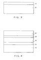
- the lower cladding layers 26, the active layer 28, and the upper cladding layer 30 are successively formed from trimethylaluminum, trimethylgallium, arsine, and hydrogen selenide, as shown in Figure 4.
- the Se-doped N-type GaAs layer 40 from which the contact layers 32 and 38 are to be made is formed on the upper cladding layer 30, as shown in Figure 5.
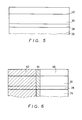
- Zn is diffused from a portion of the upper surface of the GaAs layer 40 to dope portions respectively of the GaAs layer 40, the upper cladding layer 30, the active layer 28, the lower cladding layer 26, the P-type GaAs layer 24, and the GaAs layer 22, with Zn to change these portions together into a region 42.
- Zn in the Zn-doped P-type diffusion region 42 is drive-in diffused to thereby form a Zn-drive-in-diffused P-type region 44.
- the C-doped P-type GaAs layer 24 is part of a TJS laser, but such a C-doped P-type GaAs layer can be a part of semiconductor lasers of other types, or other semiconductor light-emitting devices, such as a photodiode. It can also be formed as part of an HEMT (high electron mobility transistor) or the like. Further, in the above-described embodiment, it is a GaAs layer that is doped with carbon, but the present invention can be used to dope other compound semiconductors, such as AIGaAs, with carbon. Although, in the above-described embodiment, the Zn-drive-in-diffused P-type region is used, it is not necessarily needed.
- the Zn-diffused P -type region 34 is described to extend into a portion of the GaAs layer 22, but it may extend only as far as, for example, the P-type GaAs layer 24.
- the present invention has been described in terms of an embodiment which uses MOCVD, but it can be implemented by MOMBE.
Landscapes
- Chemical & Material Sciences (AREA)
- Engineering & Computer Science (AREA)
- Crystallography & Structural Chemistry (AREA)
- Materials Engineering (AREA)
- Metallurgy (AREA)
- Organic Chemistry (AREA)
- Physics & Mathematics (AREA)
- Inorganic Chemistry (AREA)
- Geometry (AREA)
- Condensed Matter Physics & Semiconductors (AREA)
- General Physics & Mathematics (AREA)
- Electromagnetism (AREA)
- Optics & Photonics (AREA)
- Chemical Kinetics & Catalysis (AREA)
- General Chemical & Material Sciences (AREA)
- Semiconductor Lasers (AREA)
Applications Claiming Priority (2)
| Application Number | Priority Date | Filing Date | Title |
|---|---|---|---|
| JP2270735A JPH04146680A (ja) | 1990-10-08 | 1990-10-08 | P型化合物半導体の製造方法、半導体発光装置及びその製造方法 |
| JP270735/90 | 1990-10-08 |
Publications (3)
| Publication Number | Publication Date |
|---|---|
| EP0480557A2 true EP0480557A2 (fr) | 1992-04-15 |
| EP0480557A3 EP0480557A3 (fr) | 1992-12-30 |
| EP0480557B1 EP0480557B1 (fr) | 1996-05-29 |
Family
ID=17490238
Family Applications (1)
| Application Number | Title | Priority Date | Filing Date |
|---|---|---|---|
| EP91301911A Expired - Lifetime EP0480557B1 (fr) | 1990-10-08 | 1991-03-07 | Procédé pour faire un semi-conducteur composé de type P |
Country Status (4)
| Country | Link |
|---|---|
| US (1) | US5173445A (fr) |
| EP (1) | EP0480557B1 (fr) |
| JP (1) | JPH04146680A (fr) |
| DE (1) | DE69119861T2 (fr) |
Cited By (2)
| Publication number | Priority date | Publication date | Assignee | Title |
|---|---|---|---|---|
| US5275969A (en) * | 1991-03-25 | 1994-01-04 | Mitsubishi Denki Kabushiki Kaisha | Semiconductor laser |
| EP0977245A3 (fr) * | 1998-07-27 | 2002-04-17 | Sumitomo Chemical Company, Limited | Procédé de fabrication des semi-conducteurs composés dopés au carbone |
Families Citing this family (4)
| Publication number | Priority date | Publication date | Assignee | Title |
|---|---|---|---|---|
| JP3214505B2 (ja) * | 1991-09-13 | 2001-10-02 | 株式会社デンソー | 半導体装置の製造方法 |
| JP2781097B2 (ja) * | 1992-01-30 | 1998-07-30 | 三菱電機株式会社 | 半導体装置およびその製造方法 |
| US5244829A (en) * | 1992-07-09 | 1993-09-14 | Texas Instruments Incorporated | Organometallic vapor-phase epitaxy process using (CH3)3 As and CCl4 for improving stability of carbon-doped GaAs |
| US9245993B2 (en) | 2013-03-15 | 2016-01-26 | Transphorm Inc. | Carbon doping semiconductor devices |
Family Cites Families (11)
| Publication number | Priority date | Publication date | Assignee | Title |
|---|---|---|---|---|
| JPS5511371A (en) * | 1978-07-10 | 1980-01-26 | Mitsubishi Electric Corp | Semiconductor laser system |
| US4334311A (en) * | 1980-05-13 | 1982-06-08 | Mitsubishi Denki Kabushiki Kaisha | Transverse junction stripe semiconductor laser device |
| JPS5735393A (en) * | 1980-08-11 | 1982-02-25 | Mitsubishi Electric Corp | Semiconductor laser |
| JPS5929484A (ja) * | 1982-08-12 | 1984-02-16 | Fujitsu Ltd | 半導体発光装置 |
| JPS62104118A (ja) * | 1985-10-31 | 1987-05-14 | Fujitsu Ltd | p型半導体の製造方法 |
| JPH0777200B2 (ja) * | 1986-10-02 | 1995-08-16 | 日本電信電話株式会社 | 化合物半導体装置の製造方法 |
| US4910167A (en) * | 1987-11-13 | 1990-03-20 | Kopin Corporation | III-V Semiconductor growth initiation on silicon using TMG and TEG |
| JPH01181585A (ja) * | 1988-01-12 | 1989-07-19 | Canon Inc | 半導体レーザー |
| US4935381A (en) * | 1988-12-09 | 1990-06-19 | The Aerospace Corporation | Process for growing GaAs epitaxial layers |
| JP3013992B2 (ja) * | 1989-02-01 | 2000-02-28 | 住友電気工業株式会社 | 化合物半導体結晶の成長方法 |
| JPH02273917A (ja) * | 1989-04-14 | 1990-11-08 | Fujitsu Ltd | 炭素ドープ3―v族化合物半導体の結晶成長方法 |
-
1990
- 1990-10-08 JP JP2270735A patent/JPH04146680A/ja active Pending
-
1991
- 1991-03-07 EP EP91301911A patent/EP0480557B1/fr not_active Expired - Lifetime
- 1991-03-07 DE DE69119861T patent/DE69119861T2/de not_active Expired - Lifetime
- 1991-03-20 US US07/672,448 patent/US5173445A/en not_active Expired - Lifetime
Cited By (2)
| Publication number | Priority date | Publication date | Assignee | Title |
|---|---|---|---|---|
| US5275969A (en) * | 1991-03-25 | 1994-01-04 | Mitsubishi Denki Kabushiki Kaisha | Semiconductor laser |
| EP0977245A3 (fr) * | 1998-07-27 | 2002-04-17 | Sumitomo Chemical Company, Limited | Procédé de fabrication des semi-conducteurs composés dopés au carbone |
Also Published As
| Publication number | Publication date |
|---|---|
| DE69119861T2 (de) | 1996-10-24 |
| EP0480557A3 (fr) | 1992-12-30 |
| US5173445A (en) | 1992-12-22 |
| JPH04146680A (ja) | 1992-05-20 |
| EP0480557B1 (fr) | 1996-05-29 |
| DE69119861D1 (de) | 1996-07-04 |
Similar Documents
| Publication | Publication Date | Title |
|---|---|---|
| US6233264B1 (en) | Optical semiconductor device having an active layer containing N | |
| US5831277A (en) | III-nitride superlattice structures | |
| US5834331A (en) | Method for making III-Nitride laser and detection device | |
| US4906583A (en) | Making a semiconductor photodetector | |
| US5079184A (en) | Method of manufacturing iii-iv group compound semiconductor device | |
| US6351480B1 (en) | Semiconductor light emitting device and method for producing the same | |
| USRE41310E1 (en) | Methods for growing semiconductors and devices thereof the alloy semiconductor gainnas | |
| JP2871477B2 (ja) | 半導体発光装置およびその製造方法 | |
| US4503539A (en) | Semiconductor laser | |
| US6108360A (en) | Long wavelength DH, SCH and MQW lasers based on Sb | |
| US5173445A (en) | Method of making p-type compound semiconductor employing trimethylgallium, trimethylarsenic and arsine | |
| US5146467A (en) | Semiconductor laser device | |
| EP0612128A2 (fr) | Laser à semi-conducteur et méthode de fabrication | |
| JP2960838B2 (ja) | 半導体装置及びその製造方法 | |
| US5315133A (en) | Compound semiconductor structure including p-type and n-type regions doped with carbon | |
| US5814534A (en) | Method of doping with beryllium and method of fabricating semiconductor optical element doped with beryllium | |
| US6750120B1 (en) | Method and apparatus for MOCVD growth of compounds including GaAsN alloys using an ammonia precursor with a catalyst | |
| KR100203376B1 (ko) | 수평 방향 반도체 피엔 접합 어레이 제조방법 | |
| Furuya et al. | GaInAsP/InP organometallic vapor phase epitaxy for research and fabrication of devices | |
| JP3703927B2 (ja) | 半導体レーザ素子 | |
| JP4592966B2 (ja) | Iii−v族化合物半導体結晶膜及びその成膜方法 | |
| Veuhoff | Semiconductor Layers | |
| JP4193245B2 (ja) | 化合物半導体素子 | |
| JPS61203691A (ja) | 半導体発光装置 | |
| CA2059408A1 (fr) | Fabrication de dispositifs a semiconducteur contenant de l'aluminium |
Legal Events
| Date | Code | Title | Description |
|---|---|---|---|
| PUAI | Public reference made under article 153(3) epc to a published international application that has entered the european phase |
Free format text: ORIGINAL CODE: 0009012 |
|
| AK | Designated contracting states |
Kind code of ref document: A2 Designated state(s): DE FR GB NL |
|
| PUAL | Search report despatched |
Free format text: ORIGINAL CODE: 0009013 |
|
| AK | Designated contracting states |
Kind code of ref document: A3 Designated state(s): DE FR GB NL |
|
| 17P | Request for examination filed |
Effective date: 19930125 |
|
| 17Q | First examination report despatched |
Effective date: 19940921 |
|
| GRAA | (expected) grant |
Free format text: ORIGINAL CODE: 0009210 |
|
| AK | Designated contracting states |
Kind code of ref document: B1 Designated state(s): DE FR GB NL |
|
| REF | Corresponds to: |
Ref document number: 69119861 Country of ref document: DE Date of ref document: 19960704 |
|
| ET | Fr: translation filed | ||
| PLBE | No opposition filed within time limit |
Free format text: ORIGINAL CODE: 0009261 |
|
| STAA | Information on the status of an ep patent application or granted ep patent |
Free format text: STATUS: NO OPPOSITION FILED WITHIN TIME LIMIT |
|
| 26N | No opposition filed | ||
| REG | Reference to a national code |
Ref country code: GB Ref legal event code: IF02 |
|
| PGFP | Annual fee paid to national office [announced via postgrant information from national office to epo] |
Ref country code: FR Payment date: 20060308 Year of fee payment: 16 |
|
| PGFP | Annual fee paid to national office [announced via postgrant information from national office to epo] |
Ref country code: NL Payment date: 20060315 Year of fee payment: 16 |
|
| REG | Reference to a national code |
Ref country code: GB Ref legal event code: 746 Effective date: 20070416 |
|
| NLV4 | Nl: lapsed or anulled due to non-payment of the annual fee |
Effective date: 20071001 |
|
| REG | Reference to a national code |
Ref country code: FR Ref legal event code: ST Effective date: 20071130 |
|
| PG25 | Lapsed in a contracting state [announced via postgrant information from national office to epo] |
Ref country code: NL Free format text: LAPSE BECAUSE OF NON-PAYMENT OF DUE FEES Effective date: 20071001 |
|
| PG25 | Lapsed in a contracting state [announced via postgrant information from national office to epo] |
Ref country code: FR Free format text: LAPSE BECAUSE OF NON-PAYMENT OF DUE FEES Effective date: 20070402 |
|
| PGFP | Annual fee paid to national office [announced via postgrant information from national office to epo] |
Ref country code: GB Payment date: 20100303 Year of fee payment: 20 |
|
| PGFP | Annual fee paid to national office [announced via postgrant information from national office to epo] |
Ref country code: DE Payment date: 20100318 Year of fee payment: 20 |
|
| REG | Reference to a national code |
Ref country code: DE Ref legal event code: R071 Ref document number: 69119861 Country of ref document: DE |
|
| REG | Reference to a national code |
Ref country code: GB Ref legal event code: PE20 Expiry date: 20110306 |
|
| PG25 | Lapsed in a contracting state [announced via postgrant information from national office to epo] |
Ref country code: GB Free format text: LAPSE BECAUSE OF EXPIRATION OF PROTECTION Effective date: 20110306 |
|
| PG25 | Lapsed in a contracting state [announced via postgrant information from national office to epo] |
Ref country code: DE Free format text: LAPSE BECAUSE OF EXPIRATION OF PROTECTION Effective date: 20110307 |