EP0186540A1 - Aus Dünnfilmtransistoren zusammengestellte elektronische Schaltung zur Steuerung einer Matrixeinrichtung - Google Patents
Aus Dünnfilmtransistoren zusammengestellte elektronische Schaltung zur Steuerung einer Matrixeinrichtung Download PDFInfo
- Publication number
- EP0186540A1 EP0186540A1 EP85402238A EP85402238A EP0186540A1 EP 0186540 A1 EP0186540 A1 EP 0186540A1 EP 85402238 A EP85402238 A EP 85402238A EP 85402238 A EP85402238 A EP 85402238A EP 0186540 A1 EP0186540 A1 EP 0186540A1
- Authority
- EP
- European Patent Office
- Prior art keywords
- transistors
- film transistors
- register
- matrix
- nxn
- Prior art date
- Legal status (The legal status is an assumption and is not a legal conclusion. Google has not performed a legal analysis and makes no representation as to the accuracy of the status listed.)
- Granted
Links
Images
Classifications
-
- G—PHYSICS
- G09—EDUCATION; CRYPTOGRAPHY; DISPLAY; ADVERTISING; SEALS
- G09G—ARRANGEMENTS OR CIRCUITS FOR CONTROL OF INDICATING DEVICES USING STATIC MEANS TO PRESENT VARIABLE INFORMATION
- G09G3/00—Control arrangements or circuits, of interest only in connection with visual indicators other than cathode-ray tubes
- G09G3/20—Control arrangements or circuits, of interest only in connection with visual indicators other than cathode-ray tubes for presentation of an assembly of a number of characters, e.g. a page, by composing the assembly by combination of individual elements arranged in a matrix no fixed position being assigned to or needed to be assigned to the individual characters or partial characters
- G09G3/34—Control arrangements or circuits, of interest only in connection with visual indicators other than cathode-ray tubes for presentation of an assembly of a number of characters, e.g. a page, by composing the assembly by combination of individual elements arranged in a matrix no fixed position being assigned to or needed to be assigned to the individual characters or partial characters by control of light from an independent source
- G09G3/36—Control arrangements or circuits, of interest only in connection with visual indicators other than cathode-ray tubes for presentation of an assembly of a number of characters, e.g. a page, by composing the assembly by combination of individual elements arranged in a matrix no fixed position being assigned to or needed to be assigned to the individual characters or partial characters by control of light from an independent source using liquid crystals
- G09G3/3611—Control of matrices with row and column drivers
- G09G3/3685—Details of drivers for data electrodes
- G09G3/3688—Details of drivers for data electrodes suitable for active matrices only
-
- G—PHYSICS
- G09—EDUCATION; CRYPTOGRAPHY; DISPLAY; ADVERTISING; SEALS
- G09G—ARRANGEMENTS OR CIRCUITS FOR CONTROL OF INDICATING DEVICES USING STATIC MEANS TO PRESENT VARIABLE INFORMATION
- G09G3/00—Control arrangements or circuits, of interest only in connection with visual indicators other than cathode-ray tubes
- G09G3/20—Control arrangements or circuits, of interest only in connection with visual indicators other than cathode-ray tubes for presentation of an assembly of a number of characters, e.g. a page, by composing the assembly by combination of individual elements arranged in a matrix no fixed position being assigned to or needed to be assigned to the individual characters or partial characters
-
- G—PHYSICS
- G09—EDUCATION; CRYPTOGRAPHY; DISPLAY; ADVERTISING; SEALS
- G09G—ARRANGEMENTS OR CIRCUITS FOR CONTROL OF INDICATING DEVICES USING STATIC MEANS TO PRESENT VARIABLE INFORMATION
- G09G2310/00—Command of the display device
- G09G2310/02—Addressing, scanning or driving the display screen or processing steps related thereto
- G09G2310/0264—Details of driving circuits
- G09G2310/0297—Special arrangements with multiplexing or demultiplexing of display data in the drivers for data electrodes, in a pre-processing circuitry delivering display data to said drivers or in the matrix panel, e.g. multiplexing plural data signals to one D/A converter or demultiplexing the D/A converter output to multiple columns
Definitions
- the present invention relates to an electronic circuit formed of thin film transistors used to control a matrix device.
- the invention relates to an electronic circuit of the shift register type used to sequentially control the rows or columns of a matrix device and in particular the rows or columns of a crystal display device liquids (flat screen with active matrix, screen for dashboard, ...), photosensitive video retinas with thin film transistors, optical sensors or rendering heads for fax systems with photodiodes lines, sensors, etc ...
- an electronic memory formed by memory points distributed over the entire surface of the screen stores the video signal throughout the duration of the image.
- An electro-optical transducer in particular a liquid crystal transducer, is in contact with each memory point and is excited throughout the duration of the image.
- Each memory point is located at the intersection of a line and a connection column and it consists of a thin-film transistor produced on an insulating support and a capacitor of which the armatures are made, in the case where the transducer is a liquid crystal, by the electrodes of the liquid crystal cell itself, the insulating support constituting one of the two walls of said cell.
- Each stage of the shift register generally comprises two elementary inverters and a capacitor used to store the video information.
- each inverter is formed of at least two thin film transistors, arranged in cascade.
- the thin film transistors of the active matrix are generally produced with amorphous silicon, these have a low transconductance and a high input capacity, which leads to obtaining a limit frequency of relatively low inverter operation and most of the time lower than the scanning frequency of the lines of a high complexity flat screen (300 to 500 lines).
- shift registers of the charge transfer type such as the Bucket-Brigade-Device (BBD) or the Coupled-Charge-Device (CCD) in Anglo-Saxon terminology, less greedy in number of TCM, but the density of defects in amorphous silicon has led to ineffective charge transfer.
- BBD Bucket-Brigade-Device
- CCD Coupled-Charge-Device
- the cost price of these screens is high due to the cost of the control circuits and the number of connections to be made between the flat screens and the corresponding circuits, or the number of welds to be made on the glass holder. It is generally accepted that the set of peripheral integrated circuits, that is to say the set of control circuits for the lines and the control circuits for the columns of the flat screen, represents half and even more than the price of total returns from said screen.
- the subject of the present invention is precisely an electronic circuit formed of thin film transistors used to control matrix devices and in particular flat screens with active matrix making it possible to remedy the various drawbacks mentioned above.
- peripheral integrated circuits With the active matrix while minimizing the cost of these circuits and therefore the overall price of flat screens by reducing the number of these peripheral circuits.
- the invention relates to an electronic circuit, used to control the rows or columns of a matrix device, using pa ⁇ t standard integrated circuits external to the device to provide the shift register function and d on the other hand, thin film transistors to provide the multiplexing function.
- the invention relates to an electronic control circuit with Nxn outputs used to control Nxn rows or columns of a matrix device, and in particular of a matrix display device, characterized in that it comprises a multiplexing circuit, formed by N groups of n successive thin-film transistors, a first shift register with N outputs and a second shift register with n outputs, the gates of the n transistors of the same group being connected to the same output of the first register, each group corresponding to a different output of said first register, the source of each transistor being connected to a different row or column, the drain of the i-th transistor of each group being connected to the i-th output of the second register, i being an integer such as 1 5 i n.
- matrix device can be understood a device comprising only one row or one column of components.
- These electronic control circuits only comprise two external integrated circuits, which are the two shift registers, making it possible to supply, via the multiplexing circuit, Nxn lines or columns of a matrix device and in particular of a screen. active matrix dish. This therefore makes it possible to reduce the number of connections to be made between the external circuits and the flat screen as well as to reduce the cost price of these flat screens.
- the transistors in thin layers of the multiplexing circuit of the control circuit of the invention can advantageously be produced on said support and simultaneously with the transistors of the matrix device.
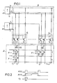
- an electronic control circuit has been shown in accordance with the invention making it possible to control Nxn lines of a flat screen with active matrix, bearing the general reference 2.
- This active matrix 2 is formed, in a conventional manner, of several conductive columns 4 and Nxn conductive lines denoted L j , j being an integer ranging from 1 to Nxn.
- L j Nxn conductive lines
- This active matrix 2 further comprises Nxn capacitors 14, one of the plates of each capacitor being connected to ground, the other to one of the conductive lines L j of the matrix 2.
- control circuit of NxN conductive lines L j of the matrix 2 is formed, on the one hand to a multiplexing circuit, of general reference 1 6, consisting of N groups G ,, ..., G N thin-film transistors, each group G i comprising n successive transistors T 1 , ... T n , and on the other hand a first shift register 18, comprising N outputs, and a second shift register 20 with n outputs.
- Such a control circuit makes it possible to considerably reduce the number of connections to be made between the control circuit and the active matrix, these connections being reduced to N + n connections instead of Nxn connections for the matrix devices of the prior art.
- each conductive line L j of the active matrix 2 is supplied by the source of a single thin film transistor; for example the source of the first transistor T, of group G, is connected to line L 1 , the source of the second transistor T 2 of group G, is connected to line L, and so on and the source of the last transistor T n of group G N at line L N. n .
- the gates of the N consecutive transistors T 1 , ... T n of the same group G; are connected to the same output P; from the first shift register 18, to each group corresponding to a different output P i from said first register.
- the gates of the transistors T 1 , ... T n of the group G, of transistors are all connected to the output P, of the first register 18, and the gates of the transistors T 1 , ... T n of the group G N of transistors are all connected to the output P N of said first register 18.
- the drains of the Nxn thin film transistors they are supplied so that the drain of the i th transistor T i of each group Ci is connected to the i th output Si of the second register 20, i being an integer such that 1 ⁇ i ⁇ not.
- the first transistors denoted T, of each group of transistors G 1 , ... G N are all connected to the first output S, of the second shift register 20, the second transistors T, of groups of transistors G 1 , ... G N are all connected to the output S2 of the second register 20, ... and the last transistors T of the groups G 1 , ... G N of transistors are all connected to the last output S n of the second register 20 .
- the signal R (n) corresponds to the output signal of the shift register 20
- the signal R (N) corresponds to the output signal of the shift register 18
- the signal L corresponds to the input signal of the first conductive line of the matrix 2.
- Each pulse of duration r, delivered by the register 20, corresponds to the access time to a conductive line of the matrix, r being close to 64 ⁇ s and the pulse r ', delivered by the register 18, is equal to nx ⁇ .
- a voltage pulse r, delivered by the shift register 18 which operates at the scanning frequency of the lines of the flat screen, will only be transmitted to a line of said screen in the group G i made passing by the pulse ⁇ ' , provided by the shift register 18.
- the corresponding lines of the flat screen are kept low thanks to the line capacitor 14 which remains charged throughout the duration of an image on the 'screen.
- the transistors 10 of the active matrix 2 are thin film transistors produced on an insulating support such as glass, constituting in particular one of the two walls of the flat screen between which is disposed the liquid crystal
- the thin film transistors of the multiplexing circuit 16 may advantageously be produced on said support and simultaneously with the manufacture of the transistors 10 of the active matrix 2 of the screen.
- the two shift registers 18 and 20 will be standard integrated circuits, produced independently of the active matrix 2.
- this manufacturing process consists in depositing, on an insulating support such as glass, constituting one of the walls of the flat screen, a transparent conductive layer in particular of tin and indium oxide and then a layer of n + doped amorphous silicon. These layers are then photo-etched using a first mask, so as to produce: the sources and drains of the thin-film transistors of the multiplexing circuit and of the matrix, one of the armatures of the capacitors 12 and 14, the conductive columns 4 of the matrix as well as the drain bus of the multiplexing circuit 16.
- a layer of hydrogenated amorphous silicon is then successively deposited, an insulating layer, in particular of silicon oxide, and a conductive layer, for example of aluminum, then a photogravure of this stack of layers is carried out, using a second mask, so as to define the gate of the thin film transistors of the multiplexing circuit 16 and of the matrix 2 as well as the conductive lines L j of said matrix.
- the assembly is then passive using a deposition of a layer of silicon oxide for example, then openings are made in this passivation layer (by photoengraving using a third mask) , at the ends of the conductive lines of the matrix, on the grids of the thin film transistors of the multiplexing circuit 16 and on the drain bus of said multiplexing circuit.
- a metallic deposit for example made of aluminum, is then produced, then the photo-engraving is carried out using a fourth mask, in order to make the connections between the multiplexing circuit 16 and the active matrix 2, between the drain bus and the drains of the thin film transistors of the multiplexing circuit and between the gates of the transistors T 1 , ... T n of the same group G i of transistors of the multiplexing circuit 16.
- the circuit of the invention can advantageously be used to control the lines of a photosensitive video retina with thin film transistors; such a retina has in particular been described in French patent application No. 82 04003 filed on March 10, 1 982 in the name of the applicant and entitled "Photoconductive element in hydrogenated amorphous silicon carbide and video retina cell using such an element".
- the circuit of the invention can be used to control a photod i odes array used in facsimile, these photodiodes and the thin film transistors of the multiplexing circuit being produced simultaneously on the same support.
- circuit of the invention can be used to control any line of electronic components of the integrated transistor or diode type.
Landscapes
- Engineering & Computer Science (AREA)
- Physics & Mathematics (AREA)
- Computer Hardware Design (AREA)
- General Physics & Mathematics (AREA)
- Theoretical Computer Science (AREA)
- Chemical & Material Sciences (AREA)
- Crystallography & Structural Chemistry (AREA)
- Liquid Crystal (AREA)
- Control Of Indicators Other Than Cathode Ray Tubes (AREA)
- Electronic Switches (AREA)
Applications Claiming Priority (2)
| Application Number | Priority Date | Filing Date | Title |
|---|---|---|---|
| FR8418110 | 1984-11-28 | ||
| FR8418110A FR2573899B1 (fr) | 1984-11-28 | 1984-11-28 | Circuit electronique forme de transistors en couches minces pour commander un dispositif matriciel |
Publications (2)
| Publication Number | Publication Date |
|---|---|
| EP0186540A1 true EP0186540A1 (de) | 1986-07-02 |
| EP0186540B1 EP0186540B1 (de) | 1989-09-06 |
Family
ID=9310015
Family Applications (1)
| Application Number | Title | Priority Date | Filing Date |
|---|---|---|---|
| EP19850402238 Expired EP0186540B1 (de) | 1984-11-28 | 1985-11-19 | Aus Dünnfilmtransistoren zusammengestellte elektronische Schaltung zur Steuerung einer Matrixeinrichtung |
Country Status (5)
| Country | Link |
|---|---|
| EP (1) | EP0186540B1 (de) |
| JP (1) | JPS61198198A (de) |
| CA (1) | CA1255406A (de) |
| DE (1) | DE3572884D1 (de) |
| FR (1) | FR2573899B1 (de) |
Cited By (5)
| Publication number | Priority date | Publication date | Assignee | Title |
|---|---|---|---|---|
| EP0318600A4 (en) * | 1987-06-19 | 1991-01-30 | Fanuc Ltd | Signal output device |
| WO1994016428A1 (en) * | 1993-01-05 | 1994-07-21 | Yuen Foong Yu H.K. Co., Ltd. | A data driver circuit for use with an lcd display |
| EP0740285A3 (de) * | 1995-04-27 | 1997-12-03 | Canon Kabushiki Kaisha | Datenübertragungsverfahren für eine Anzeigesteuerschaltung |
| WO1999046753A1 (fr) * | 1998-03-10 | 1999-09-16 | Thomson-Lcd | Procede d'affichage de donnees sur afficheur matriciel avec ordre de balayage alterne en groupes adjacents de colonnes |
| FR2776108A1 (fr) * | 1998-03-10 | 1999-09-17 | Thomson Lcd | Procede d'affichage de donnees sur un afficheur matriciel |
Citations (1)
| Publication number | Priority date | Publication date | Assignee | Title |
|---|---|---|---|---|
| FR2260919A1 (de) * | 1974-02-07 | 1975-09-05 | Nippon Electric Co |
-
1984
- 1984-11-28 FR FR8418110A patent/FR2573899B1/fr not_active Expired
-
1985
- 1985-11-19 DE DE8585402238T patent/DE3572884D1/de not_active Expired
- 1985-11-19 EP EP19850402238 patent/EP0186540B1/de not_active Expired
- 1985-11-28 CA CA000496472A patent/CA1255406A/en not_active Expired
- 1985-11-28 JP JP60268275A patent/JPS61198198A/ja active Pending
Patent Citations (1)
| Publication number | Priority date | Publication date | Assignee | Title |
|---|---|---|---|---|
| FR2260919A1 (de) * | 1974-02-07 | 1975-09-05 | Nippon Electric Co |
Non-Patent Citations (1)
| Title |
|---|
| 1982 SID INTERNATIONAL SYMPOSIUM, DIGEST OF TECHNICAL PAPERS, première édition, mai 1982, pages 266-267, Lewis Winner, Coral Gables, US; K.-I. OKI et al.: "MOS-EL integrated display device" * |
Cited By (9)
| Publication number | Priority date | Publication date | Assignee | Title |
|---|---|---|---|---|
| EP0318600A4 (en) * | 1987-06-19 | 1991-01-30 | Fanuc Ltd | Signal output device |
| WO1994016428A1 (en) * | 1993-01-05 | 1994-07-21 | Yuen Foong Yu H.K. Co., Ltd. | A data driver circuit for use with an lcd display |
| US5510807A (en) * | 1993-01-05 | 1996-04-23 | Yuen Foong Yu H.K. Co., Ltd. | Data driver circuit and associated method for use with scanned LCD video display |
| EP0740285A3 (de) * | 1995-04-27 | 1997-12-03 | Canon Kabushiki Kaisha | Datenübertragungsverfahren für eine Anzeigesteuerschaltung |
| US6078318A (en) * | 1995-04-27 | 2000-06-20 | Canon Kabushiki Kaisha | Data transfer method, display driving circuit using the method, and image display apparatus |
| US6335720B1 (en) | 1995-04-27 | 2002-01-01 | Canon Kabushiki Kaisha | Data transfer method, display driving circuit using the method, and image display apparatus |
| WO1999046753A1 (fr) * | 1998-03-10 | 1999-09-16 | Thomson-Lcd | Procede d'affichage de donnees sur afficheur matriciel avec ordre de balayage alterne en groupes adjacents de colonnes |
| FR2776108A1 (fr) * | 1998-03-10 | 1999-09-17 | Thomson Lcd | Procede d'affichage de donnees sur un afficheur matriciel |
| US6924785B1 (en) | 1998-03-10 | 2005-08-02 | Thales Avionics Lcd S.A. | Method and apparatus for displaying data on a matrix display with an alternating order of scanning in adjacent groups of columns |
Also Published As
| Publication number | Publication date |
|---|---|
| CA1255406A (en) | 1989-06-06 |
| DE3572884D1 (en) | 1989-10-12 |
| FR2573899B1 (fr) | 1986-12-26 |
| EP0186540B1 (de) | 1989-09-06 |
| FR2573899A1 (fr) | 1986-05-30 |
| JPS61198198A (ja) | 1986-09-02 |
Similar Documents
| Publication | Publication Date | Title |
|---|---|---|
| EP0586398B1 (de) | Shiftregister zum abtasten der ansteurungsleitungen zur verwendung bei einer flüssigkristallanzeige | |
| EP1419533B1 (de) | Aktive matrix von dünnfilmtransistoren (tft) für einen optischen sensor oder einen anzeigeschirm | |
| EP0216673B1 (de) | Verfahren zur Herstellung eines Schalttransistors für einen flachen Bildschirm und nach diesem Verfahren hergestelltes Schaltelement | |
| FR2488013A1 (fr) | Dispositif a matrice d'elements actifs | |
| EP0245147A1 (de) | Röntgen-Bilderfassungstafel und deren Herstellungsverfahren | |
| FR2593343A1 (fr) | Matrice d'elements photosensibles et son procede de fabrication, procede de lecture associe, et application de cette matrice a la prise de vue d'images | |
| FR2737938A1 (fr) | Dispositif d'affichage a cristaux liquides et un procede de fabrication d'un tel dispositif | |
| EP0148654A1 (de) | Fotoempfindliche Anordnung für Infrarot | |
| FR2805650A1 (fr) | Procede de compensation d'un circuit capacitif perturbe et application aux ecrans de visualisation matriciels | |
| EP0143039A1 (de) | Herstellungsverfahren einer Anordnung elektronischer Bauteile | |
| FR2533072A1 (fr) | Procede de fabrication de circuits electroniques a base de transistors en couches minces et de condensateurs | |
| EP2708023B1 (de) | Vorrichtung zur adressierung von leitungen eines steuerkreises für eine aktive detektionsmatrix | |
| EP0145520A2 (de) | Bildschirm mit aktiver Matrix ohne Kreuzung von Zeilen- und Spaltenadressenleitungen | |
| EP0228317B1 (de) | Elektrooptischer Anzeigeschirm mit Steuertransistoren | |
| FR2700050A1 (fr) | Matrice active pour affichages à cristaux liquides. | |
| EP0506528B1 (de) | Matrix-Ansteuerungsstruktur für Anzeigeschirm | |
| EP0186540B1 (de) | Aus Dünnfilmtransistoren zusammengestellte elektronische Schaltung zur Steuerung einer Matrixeinrichtung | |
| US4819082A (en) | Manuscript reading device | |
| EP0197992B1 (de) | Anzeigevorrichtung mit aktiver matrix, angesteuert durch transistorenpaare | |
| EP0368733B1 (de) | Herstellungsprozess für einen Anzeigebildschirm mit einer Transistormatrix, versehen mit einer lichtundurchlässigen Maske | |
| EP0129470B1 (de) | Festkörper photoempfindliche Anordnung | |
| FR2488016A1 (fr) | Module elementaire pour panneau d'affichage matriciel et panneau d'affichage comportant un tel module | |
| EP0275740B1 (de) | Ausleseschaltung für eine lichtempfindliche Zeilenübertragungsanordnung, lichtempfindliche Zeilenübertragungsanordnung mit einer solchen Schaltung und Ausleseverfahren einer solchen Anordnung | |
| FR2616270A1 (fr) | Reseau de transistors predeposes, procede de realisation de ce reseau et d'un circuit electronique au moyen de ce reseau | |
| JPS5821864A (ja) | 薄膜半導体装置の製造方法 |
Legal Events
| Date | Code | Title | Description |
|---|---|---|---|
| PUAI | Public reference made under article 153(3) epc to a published international application that has entered the european phase |
Free format text: ORIGINAL CODE: 0009012 |
|
| AK | Designated contracting states |
Kind code of ref document: A1 Designated state(s): CH DE GB IT LI NL |
|
| 17P | Request for examination filed |
Effective date: 19861204 |
|
| RAP1 | Party data changed (applicant data changed or rights of an application transferred) |
Owner name: ETAT FRANCAIS REPRESENTE PAR LE MINISTRE DES PTT ( |
|
| 17Q | First examination report despatched |
Effective date: 19890124 |
|
| GRAA | (expected) grant |
Free format text: ORIGINAL CODE: 0009210 |
|
| AK | Designated contracting states |
Kind code of ref document: B1 Designated state(s): CH DE GB IT LI NL |
|
| REF | Corresponds to: |
Ref document number: 3572884 Country of ref document: DE Date of ref document: 19891012 |
|
| ITF | It: translation for a ep patent filed | ||
| GBT | Gb: translation of ep patent filed (gb section 77(6)(a)/1977) | ||
| PLBI | Opposition filed |
Free format text: ORIGINAL CODE: 0009260 |
|
| 26 | Opposition filed |
Opponent name: BSG TECHNISCHE BERATUNGS-GESELLSCHAFT MBH Effective date: 19900606 |
|
| NLR1 | Nl: opposition has been filed with the epo |
Opponent name: BSG TECHNISCHE BERATUNGS-GESELLSCHAFT MBH. |
|
| PGFP | Annual fee paid to national office [announced via postgrant information from national office to epo] |
Ref country code: DE Payment date: 19901015 Year of fee payment: 6 |
|
| PGFP | Annual fee paid to national office [announced via postgrant information from national office to epo] |
Ref country code: GB Payment date: 19901112 Year of fee payment: 6 Ref country code: CH Payment date: 19901112 Year of fee payment: 6 |
|
| ITTA | It: last paid annual fee | ||
| PGFP | Annual fee paid to national office [announced via postgrant information from national office to epo] |
Ref country code: NL Payment date: 19901130 Year of fee payment: 6 |
|
| RDAG | Patent revoked |
Free format text: ORIGINAL CODE: 0009271 |
|
| STAA | Information on the status of an ep patent application or granted ep patent |
Free format text: STATUS: PATENT REVOKED |
|
| 27W | Patent revoked |
Effective date: 19910420 |
|
| GBPR | Gb: patent revoked under art. 102 of the ep convention designating the uk as contracting state | ||
| REG | Reference to a national code |
Ref country code: CH Ref legal event code: PL |
|
| NLR2 | Nl: decision of opposition |