EP0186851A2 - Appareil et méthode pour la formation d'une image composite par faisceau d'électrons balayé - Google Patents
Appareil et méthode pour la formation d'une image composite par faisceau d'électrons balayé Download PDFInfo
- Publication number
- EP0186851A2 EP0186851A2 EP85116115A EP85116115A EP0186851A2 EP 0186851 A2 EP0186851 A2 EP 0186851A2 EP 85116115 A EP85116115 A EP 85116115A EP 85116115 A EP85116115 A EP 85116115A EP 0186851 A2 EP0186851 A2 EP 0186851A2
- Authority
- EP
- European Patent Office
- Prior art keywords
- detector
- electron beam
- electrons
- signal
- accordance
- Prior art date
- Legal status (The legal status is an assumption and is not a legal conclusion. Google has not performed a legal analysis and makes no representation as to the accuracy of the status listed.)
- Granted
Links
- 238000010894 electron beam technology Methods 0.000 title claims abstract description 33
- 239000002131 composite material Substances 0.000 title claims abstract description 26
- 238000000034 method Methods 0.000 title claims description 16
- 230000015572 biosynthetic process Effects 0.000 title description 2
- 239000004065 semiconductor Substances 0.000 claims description 8
- 238000012545 processing Methods 0.000 claims description 5
- 239000000463 material Substances 0.000 claims description 4
- 230000000007 visual effect Effects 0.000 claims 2
- 238000004519 manufacturing process Methods 0.000 claims 1
- 238000010586 diagram Methods 0.000 description 5
- 238000005259 measurement Methods 0.000 description 4
- 239000000758 substrate Substances 0.000 description 4
- 238000004626 scanning electron microscopy Methods 0.000 description 3
- 238000006073 displacement reaction Methods 0.000 description 2
- 230000000694 effects Effects 0.000 description 2
- 230000006870 function Effects 0.000 description 2
- 238000010884 ion-beam technique Methods 0.000 description 2
- 150000002500 ions Chemical class 0.000 description 2
- 238000004125 X-ray microanalysis Methods 0.000 description 1
- XAGFODPZIPBFFR-UHFFFAOYSA-N aluminium Chemical compound [Al] XAGFODPZIPBFFR-UHFFFAOYSA-N 0.000 description 1
- 229910052782 aluminium Inorganic materials 0.000 description 1
- 238000004458 analytical method Methods 0.000 description 1
- 238000005513 bias potential Methods 0.000 description 1
- 238000000576 coating method Methods 0.000 description 1
- 230000007423 decrease Effects 0.000 description 1
- 238000001514 detection method Methods 0.000 description 1
- 238000010191 image analysis Methods 0.000 description 1
- 238000011835 investigation Methods 0.000 description 1
- 238000004969 ion scattering spectroscopy Methods 0.000 description 1
- 238000001000 micrograph Methods 0.000 description 1
- 230000003287 optical effect Effects 0.000 description 1
- 229920002120 photoresistant polymer Polymers 0.000 description 1
- 238000011160 research Methods 0.000 description 1
- 238000012827 research and development Methods 0.000 description 1
- 238000001878 scanning electron micrograph Methods 0.000 description 1
- 229910052710 silicon Inorganic materials 0.000 description 1
- 239000010703 silicon Substances 0.000 description 1
- 239000007787 solid Substances 0.000 description 1
- 239000011800 void material Substances 0.000 description 1
Images


Classifications
-
- H—ELECTRICITY
- H01—ELECTRIC ELEMENTS
- H01J—ELECTRIC DISCHARGE TUBES OR DISCHARGE LAMPS
- H01J37/00—Discharge tubes with provision for introducing objects or material to be exposed to the discharge, e.g. for the purpose of examination or processing thereof
- H01J37/26—Electron or ion microscopes; Electron or ion diffraction tubes
- H01J37/28—Electron or ion microscopes; Electron or ion diffraction tubes with scanning beams
Definitions
- This invention relates generally to the field of scanning electron microscopes (SEM) and, more particularly, to an SEM apparatus and a method for scanning an electron beam across a topographical feature on a planar surface and detecting resulting secondary electrons which are collected by a pair of oppositely disposed electron detectors which are alternately switched on and off to produce first and second electric signals which are combined to produce a composite electric signal which provides an enhanced, symmetrical image of the junctures of the planar surface with the opposite lower edges of the topographical feature, which enhanced image can be used to determine very small widths of topographical features such as very narrow conductive coatings on a semiconductor substrate.
- SEM scanning electron microscopes
- An E-T detector is generally cylindrical in shape and contains a scintillator material which converts impinging electrons to photons which are conducted to a photomultiplier which produces an electric signal corresponding to the intensity of the collected electrons.
- E-T detector When an electron beam strikes the surface of a specimen, both secondary electrons and backscattered (reflected) beam electrons escape the specimen. Secondary electrons are emitted with an average energy of 3-5 eV.
- the electron beam has an energy of, for example, 20 keV, and the backscattered beam electrons have a much higher energy than the secondary electrons which are emitted.
- the backscattered electrons are highly directional, and their directions are not affected by the positive bias voltage on the Faraday cage of an E-T detector.
- the cage bias voltage is not required, as the E-T detector will collect all backscattered electrons whose take- off angles are within the range of the detector's solid angle of collection.
- a positive bias potential up to as + 300 V is placed on the Faraday cage.
- Jackman has described the use of a plurality of E-T detectors for detecting backscattered beam electrons. Through the use of optical switches, the signals from these detectors can be viewed individually to give asymmetric detection, summed to give the equivalent of a large symmetric detector, or subtracted (Jackman, J., June 19, 1980; Industrial Research and Development. Vol. 22, page 115).
- Sa i tou et al. have described a digital computer-controlled electron beam microfabrication system for recording submircometer patterns by an electron resist on a semiconductor wafer. Registration of the beam is achieved by detecting backscattered electrons to locate the positions of registration or reference marks on the wafer. (Journal of Physics . SectE, Scientific instruments. Vol. 7, Jan. 1974, pages 441-444).
- Schur et aI have described an SEM including a modified E-T scintillator-photomultiplier for detecting backscattered electrons in quantitative image analysis (stereology) of plane-polished sections.
- Reimer in US-A-4,308,457 has described an electron microscope in which an electron beam impinges upon a specimen, and including a detector for separately detecting the secondary electrons released from a specimen and the secondary electrons produced by the beam electrons backscattered from the specimen.
- Van Nieuwland et sl. in US-A-3,920,990 have described an ion-scattering spectrometer including an ion beam source for directing an ion beam onto the surface of a material to be analyzed, a diaphragm- aperture for passing ions backscattered from the surface only at a particular angle, and a detector for measuring the kinetic energy of the passed backscattered ions.
- the primary object of the invention is to provide an improved apparatus and method for obtaining an enhanced and symmetrical electric signal image of the bottom edges of a structure projecting from a planar surface.
- Another related object is to provide such an apparatus and method for determining very small line widths of a topographical feature on a semiconductor substrate.
- the electron beam is transversely scanned along the same line with the one detector OFF and the other detector ON to produce a second electric signal whose waveform shows a pronounced amplitude change produced by secondary electrons collected from the structure's other bottom edge which is now the more remote from the ON detector.
- the two electric signals are combined to produce a composite electric signal having a waveform which has enhanced and symmetrical amplitude changes accurately corresponding to the two bottom edges of the structure.
- the composite signal may be fed to a CRT monitor for observing the image of the structure, or processed and then fed to a computer automated line-width measurement algorithm to produce a line width measurement.
- the electron beam is chosen to be of sufficiently low energy such that the specimen, such as a semiconductor, being scanned is not damaged by the beam.
- a positive bias voltage is placed on the Faraday cages of the two E-T detectors, and the image of the back or remote side of the structure is produced predominately by secondary electrons emitted from this back or remote side.
- the structure itself, "shades" or blocks from the more remote detector any beam electrons which are backscattered from the remote or back side of the structure. Because of the bias on each of the opposing detectors, it may be necessary to calibrate the digital scan line so that any beam displacement due to the opposing detectors is nullified.
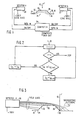
- Fig. 1 is a schematic diagram illustrating the physical relationships of the components of the apparatus of the invention and also illustrating the method of the invention. More specifically, an electron beam 10 from an SEM scans in a transverse direction a specimen 14 shown in cross section.
- This specimen consists of a substrate 16 having a planar surface 18 from which protrudes a longitudinally extending structure or topographical feature 20.
- the structure or feature 20 has a lefthand edge 22 forming a juncture 24 with the planar surface 18, and a righthand edge 26 forming a juncture 28 with the planar surface 18.
- the edges 22 and 26 are illustrated as slanted edges, but they may be vertical. It is known that the number of secondary electrons emitted by a surface struck by an electron beam is at a maximum for surfaces parallel to the beam, decreases for surfaces perpendicular to the beam and is at a minimum at junctures 24 and 28.
- E-T scintillator-photomultiplier detectors 30 and 32 are disposed within an SEM such that their respective longitudinal axes are parallel to the planar surface and such that they are located on transversely opposite sides, respectively, of the longitudinally extending structure 20.
- the E-T detector 30 on the left side is designated detector A
- the E-T detector 32 on the right side is designated as detector B. Since this invention depends upon the collection of secondary electrons, up to + 300 V bias is applied to the Faraday cage of each of the detectors 30 and 32.
- a computer 34 controls the On/Off operation of the detector 30 and 32 in accordance with this invention, receives from both of the detectors 30 and 32 data in the form of electric signals representing the intensity of the electrons collected by the respective detectors, and processes this data to output composite data in the form of either an enhanced and symmetrical minimum composite signal representing the image of the scanned structure or else as a line-width signal, as will be described in more detail below.
- the SEM For semiconductor specimens and other specimens which may be damaged by the relatively high electron beam energy of a conventional SEM, the SEM must be designed to have an electron beam energy of 2.5 keV or below. Such specimens would be, for example, silicon, aluminum, photoresist, etc. However, for specimens which would not be damaged by high energy scanning electron beams, the invention is just as applicable to electron beams of 25-30 keV as found in a conventional SEM used for specimen analysis. Furthermore, even though detectors 30 and 32 are shown as being parallel to the planar surface 18, their actual orientations are determined by the SEM manufacturer and are not critical to the operation of this invention. In a typical SEM, the detectors 30 and 32 would be fixed, and the specimen is appropriately positioned between the detectors for transverse scanning by the electron beam 10. Furthermore, even though the cage bias is illustrated as being + 3 0 0 V, it may be any positive voltage up to + 300 V.
- the method of this invention and the operation of the apparatus illustrated in Fig. 1 are based on the novel principle of forming an enhanced and symmetrical composite image of the structure's side edges by utilizing only the data signals from the respective sides of the structure which face away, or are more remote, from the ON E-T detector.
- this principle is achieved by transversely scanning along a line with only one of the detectors 30 and 32 ON, and then scanning along the same line with only the other detector ON. It was discovered that the resulting waveforms from detectors A and B each have a pronounced or enhanced dip in amplitude at the point corresponding to the structure's bottom edge which is the more remote from the ON detector.
- the signal waveforms from the two detectors are then combined in accordance with an algorithm illustrated by the flow chart of Fig. 2 to produce a minimum composite signal having symmetrical and enhanced or pronounced dips corresponding exactly to the junctures 24 and 28 of the structure's bottom edges with the planar surface 18 of specimen 14.
- the apparatus shown in Fig. 1 will perform the function of forming a symmetrical composite image which utilizes only the detector signal corresponding to the secondary electrons collected from the structure's side facing away from the ON E-T detector and the usual signal from the surfaces not obstructed by roughness.
- the computer 34 first switches ON one of the two opposing E-T detectors 30 and 32 and collects an array of digital image intensity values as a function of beam position. The computer then switches OFF this detector and switches ON the opposite detector to collect another array of digitial values, each of which corresponds positionally to the values in the first array.
- the composite "shadow" edge image is formed by comparing the corresponding array values from the two detectors 30 and 32 and then storing the lower or minimum of the two values in a third array; if the two values are equal, the computer stores either of the two values, as illustrated by the flow chart of Fig. 2 in which I Ai is the intensity value from and stored at position or address i from detector A, I Bi is the equivalent information from detector B (when detector B is ON), k is a calibration constant for any offset beam displacement due to detector bias, and I Ci is the composite image array.
- Fig. 4 shows the relationship between the cross-section of structure 20, the stored signals from the detectors A and B, and the composite signals formed by the practice of this invention.
- Waveform A represents the signal output from detector A (when detector A is ON) and has a pronounced dip 40 or reduction in amplitude at the point corresponding to the bottom edge or juncture 28 of the edge 26 and the planar surface 18, the edge 26 facing away from the ON detector 30.
- waveform B represents the signal from detector B from the next transverse scan (when detector B is ON, and detector A is OFF); here, the dip 42 corresponds to the juncture 24 of the edge 22 and the planar surface 18, the edge 22 facing away from the ON detector B.
- Waveform C represents the enhanced and symmetrical minimum composite signal formed by combining waveforms A and B in accordance with the foregoing algorithm; i.e., waveform C is formed by choosing at each point thereof the lower of the corresponding values of waveforms A and B. If desired, a maximum composite signal waveform D may be formed by choosing the higher of the values of waveforms A and B.
- Fig. 5 is a schematic block diagram illustrating typical components required for alternately switching ON and OFF the detectors A and B and for storing the detector data signals in a RAM which also stores the necessary algorithms.
- a high voltage relay 46 has a normally closed lower contact 48 which normally supplies the operating and bias voltages to detector B.
- the analog signal from detector B is converted to a digital signal by an A/D converter 38 and fed to an I/O port 44 which outputs a logical "1" signal on line 50 to open relay contact 48 and close the upper relay contact 54, thereby supplying operating voltage to detector A.
- the detectors are alternately switched ON and OFF for successive scans of the electron beam of the SEM to provide the detector operation required for this invention.
- the signals are stored in the read-only memory RAM 52 and the microprocessor unit MPU 56 provides the signal processing/combining operation described above to produce either an image signal or a line-width measurement.
- this invention solves two distinct problems: It removes the detector-induced signal asymmetry of the prior art and allows for the enhancement of the image of the bottom edge of both sides of a scanned structure for computer-automated line width measurements.
- Essential features of the invention are that the detectors A and B be located on transverely opposite sides of the structure being scanned and that the detectors be alternately switched ON and OFF for successive scans as described above.
- the intensity value for each scan position is stored in a corresponding RAM location for each detector.
- the signal outputs from the two detectors are compared at each location to form a new composite minimum or maximum signal depending upon the desired results. This composite signal image is virtually independent of bias due to the detectors (in the axis of detector orientation).
Landscapes
- Chemical & Material Sciences (AREA)
- Analytical Chemistry (AREA)
- Analysing Materials By The Use Of Radiation (AREA)
- Length-Measuring Devices Using Wave Or Particle Radiation (AREA)
Applications Claiming Priority (2)
| Application Number | Priority Date | Filing Date | Title |
|---|---|---|---|
| US687887 | 1984-12-31 | ||
| US06/687,887 US4588890A (en) | 1984-12-31 | 1984-12-31 | Apparatus and method for composite image formation by scanning electron beam |
Publications (3)
| Publication Number | Publication Date |
|---|---|
| EP0186851A2 true EP0186851A2 (fr) | 1986-07-09 |
| EP0186851A3 EP0186851A3 (en) | 1986-10-08 |
| EP0186851B1 EP0186851B1 (fr) | 1989-10-04 |
Family
ID=24762281
Family Applications (1)
| Application Number | Title | Priority Date | Filing Date |
|---|---|---|---|
| EP85116115A Expired EP0186851B1 (fr) | 1984-12-31 | 1985-12-17 | Appareil et méthode pour la formation d'une image composite par faisceau d'électrons balayé |
Country Status (4)
| Country | Link |
|---|---|
| US (1) | US4588890A (fr) |
| EP (1) | EP0186851B1 (fr) |
| JP (1) | JPS61161644A (fr) |
| DE (1) | DE3573489D1 (fr) |
Cited By (2)
| Publication number | Priority date | Publication date | Assignee | Title |
|---|---|---|---|---|
| US4941980A (en) * | 1989-02-17 | 1990-07-17 | Opal, Inc. | System for measuring a topographical feature on a specimen |
| GB2247345A (en) * | 1990-07-05 | 1992-02-26 | Haroon Ahmed | Integrated circuit structure analysis. |
Families Citing this family (20)
| Publication number | Priority date | Publication date | Assignee | Title |
|---|---|---|---|---|
| JPS6190161A (ja) * | 1984-10-09 | 1986-05-08 | Seiko Instr & Electronics Ltd | 集束イオンビ−ムのビ−ム形状調整方法 |
| JPS62190405A (ja) * | 1986-02-17 | 1987-08-20 | Hitachi Ltd | 電子ビ−ム測長装置 |
| JPH07122574B2 (ja) * | 1986-07-25 | 1995-12-25 | 株式会社日立製作所 | 断面形状測定方法 |
| JP2786207B2 (ja) * | 1988-08-26 | 1998-08-13 | 株式会社日立製作所 | 走査型顕微鏡における表面形状算出方法 |
| US5212383A (en) * | 1991-07-29 | 1993-05-18 | David Scharf | Color synthesizing scanning electron microscope |
| JP2823450B2 (ja) * | 1992-11-19 | 1998-11-11 | 株式会社東芝 | 回路パターンの寸法測定方法 |
| JP2734337B2 (ja) * | 1993-05-19 | 1998-03-30 | 日本電気株式会社 | 信号合成方法および装置 |
| US5493116A (en) * | 1993-10-26 | 1996-02-20 | Metrologix, Inc. | Detection system for precision measurements and high resolution inspection of high aspect ratio structures using particle beam devices |
| US5586321A (en) * | 1995-02-21 | 1996-12-17 | Ramot Ltd. | Diffracting token router and applications thereof |
| US6023060A (en) * | 1998-03-03 | 2000-02-08 | Etec Systems, Inc. | T-shaped electron-beam microcolumn as a general purpose scanning electron microscope |
| US6630667B1 (en) | 2000-09-29 | 2003-10-07 | Nptest, Llc | Compact, high collection efficiency scintillator for secondary electron detection |
| WO2002049080A2 (fr) * | 2000-12-15 | 2002-06-20 | Kla Tencor Corporation | Procédé et dispositif d'examen de substrat |
| US6815675B1 (en) * | 2003-04-30 | 2004-11-09 | Kla-Tencor Technologies Corporation | Method and system for e-beam scanning |
| US7531812B2 (en) * | 2003-10-27 | 2009-05-12 | Politechnika Wroclawska | Method and system for the directional detection of electrons in a scanning electron microscope |
| PL210038B1 (pl) * | 2004-01-21 | 2011-11-30 | Politechnika Wroclawska | Sposób i układ do kierunkowej detekcji elektronów w skaningowym mikroskopie elektronowym |
| US7135678B2 (en) * | 2004-07-09 | 2006-11-14 | Credence Systems Corporation | Charged particle guide |
| US7241991B1 (en) | 2005-08-30 | 2007-07-10 | Kla-Tencor Technologies Corporation | Region-of-interest based electron beam metrology |
| JP5099291B2 (ja) * | 2006-02-14 | 2012-12-19 | エスアイアイ・ナノテクノロジー株式会社 | 集束イオンビーム装置及び試料の断面加工・観察方法 |
| US7952073B2 (en) * | 2008-08-01 | 2011-05-31 | Direct Electron, Lp | Apparatus and method including a direct bombardment detector and a secondary detector for use in electron microscopy |
| JP5530959B2 (ja) * | 2011-02-28 | 2014-06-25 | 株式会社アドバンテスト | パターン高さ測定装置及びパターン高さ測定方法 |
Family Cites Families (12)
| Publication number | Priority date | Publication date | Assignee | Title |
|---|---|---|---|---|
| US3329813A (en) * | 1964-08-25 | 1967-07-04 | Jeol Ltd | Backscatter electron analysis apparatus to determine elemental content or surface topography of a specimen |
| US3549999A (en) * | 1968-06-05 | 1970-12-22 | Gen Electric | Method and apparatus for testing circuits by measuring secondary emission electrons generated by electron beam bombardment of the pulsed circuit |
| NL7306378A (fr) * | 1973-05-08 | 1974-11-12 | ||
| JPS5910688Y2 (ja) * | 1977-09-14 | 1984-04-03 | 富士通株式会社 | 電子検出器 |
| JPS5481075A (en) * | 1977-11-24 | 1979-06-28 | Cho Lsi Gijutsu Kenkyu Kumiai | Method of detecting article image using electron beam |
| US4217495A (en) * | 1978-04-18 | 1980-08-12 | Robinson Vivian N E | Electron microscope backscattered electron detectors |
| DE2921151C2 (de) * | 1979-05-25 | 1982-12-02 | Ernst Leitz Wetzlar Gmbh, 6330 Wetzlar | Vorrichtung zum Nachweis von in einem Abtast-Elektronenstrahlmikroskop von einer Probe ausgehenden Rückstreuelektronen |
| JPS59112217A (ja) * | 1982-11-29 | 1984-06-28 | Toshiba Corp | 寸法測定方法 |
| JPS59163506A (ja) * | 1983-03-09 | 1984-09-14 | Hitachi Ltd | 電子ビ−ム測長装置 |
| JPS59165357A (ja) * | 1983-03-09 | 1984-09-18 | Hitachi Ltd | 走査形電子顕微鏡の像形成方法 |
| US4535249A (en) * | 1983-06-17 | 1985-08-13 | Hughes Aircraft Company | Benchmark detector |
| JPH0643885B2 (ja) * | 1984-05-25 | 1994-06-08 | 株式会社日立製作所 | 荷電粒子マイクロプロ−ブ装置 |
-
1984
- 1984-12-31 US US06/687,887 patent/US4588890A/en not_active Expired - Fee Related
-
1985
- 1985-08-14 JP JP60177792A patent/JPS61161644A/ja active Pending
- 1985-12-17 DE DE8585116115T patent/DE3573489D1/de not_active Expired
- 1985-12-17 EP EP85116115A patent/EP0186851B1/fr not_active Expired
Cited By (3)
| Publication number | Priority date | Publication date | Assignee | Title |
|---|---|---|---|---|
| US4941980A (en) * | 1989-02-17 | 1990-07-17 | Opal, Inc. | System for measuring a topographical feature on a specimen |
| GB2247345A (en) * | 1990-07-05 | 1992-02-26 | Haroon Ahmed | Integrated circuit structure analysis. |
| GB2247345B (en) * | 1990-07-05 | 1995-04-05 | Haroon Ahmed | Integrated circuit structure analysis |
Also Published As
| Publication number | Publication date |
|---|---|
| EP0186851A3 (en) | 1986-10-08 |
| DE3573489D1 (en) | 1989-11-09 |
| EP0186851B1 (fr) | 1989-10-04 |
| JPS61161644A (ja) | 1986-07-22 |
| US4588890A (en) | 1986-05-13 |
Similar Documents
| Publication | Publication Date | Title |
|---|---|---|
| US4588890A (en) | Apparatus and method for composite image formation by scanning electron beam | |
| US8766182B2 (en) | Method for detecting information of an electric potential on a sample and charged particle beam apparatus | |
| US6791084B2 (en) | Method and scanning electron microscope for measuring dimension of material on sample | |
| US5493116A (en) | Detection system for precision measurements and high resolution inspection of high aspect ratio structures using particle beam devices | |
| US4941980A (en) | System for measuring a topographical feature on a specimen | |
| US5408098A (en) | Method and apparatus for detecting low loss electrons in a scanning electron microscope | |
| US8487253B2 (en) | Scanning electron microscope | |
| JPH09320505A (ja) | 電子線式検査方法及びその装置並びに半導体の製造方法及びその製造ライン | |
| CA1103813A (fr) | Appareil pour lithographie a faisceau electronique | |
| EP0669538A2 (fr) | Procédé pour mesurer un champ magnétique et dispositif à faisceau de particules chargées utilisant ce procédé | |
| US4677296A (en) | Apparatus and method for measuring lengths in a scanning particle microscope | |
| US6603120B2 (en) | Test method of mask for electron-beam exposure and method of electron-beam exposure | |
| Czepkowshi et al. | Some limitations of surface profile reconstruction in scanning electron microscopy | |
| US5712488A (en) | Electron beam performance measurement system and method thereof | |
| EP0335398A1 (fr) | Microscope électronique de balayage pour observer et mesurer des petits dessins d'échantillons | |
| Rosenfield | Analysis of linewidth measurement techniques using the low voltage SEM | |
| JP2001148016A (ja) | 試料検査装置,試料表示装置、および試料表示方法 | |
| JP2001093950A (ja) | 半導体パターン検査装置および半導体パターン検査方法 | |
| Slówko | Directional detection of secondary electrons for electron beam profilography | |
| US6969853B2 (en) | Pattern width measuring apparatus, pattern width measuring method, and electron beam exposure apparatus | |
| WO1996008835A1 (fr) | Detecteur de faisceaux de particules permettant d'obtenir un contraste topographique et dans les trois dimensions | |
| JP3608451B2 (ja) | 走査電子顕微鏡を用いた検査装置および検査方法 | |
| Postek | Nondestructive submicron dimensional metrology using the scanning electron microscope | |
| JPH07286842A (ja) | 寸法検査方法及びその装置 | |
| JP2557847B2 (ja) | 半導体集積回路の動作解析方法及び動作解析装置 |
Legal Events
| Date | Code | Title | Description |
|---|---|---|---|
| PUAI | Public reference made under article 153(3) epc to a published international application that has entered the european phase |
Free format text: ORIGINAL CODE: 0009012 |
|
| AK | Designated contracting states |
Kind code of ref document: A2 Designated state(s): DE FR GB |
|
| PUAL | Search report despatched |
Free format text: ORIGINAL CODE: 0009013 |
|
| AK | Designated contracting states |
Kind code of ref document: A3 Designated state(s): DE FR GB |
|
| 17P | Request for examination filed |
Effective date: 19861029 |
|
| 17Q | First examination report despatched |
Effective date: 19880309 |
|
| GRAA | (expected) grant |
Free format text: ORIGINAL CODE: 0009210 |
|
| AK | Designated contracting states |
Kind code of ref document: B1 Designated state(s): DE FR GB |
|
| REF | Corresponds to: |
Ref document number: 3573489 Country of ref document: DE Date of ref document: 19891109 |
|
| ET | Fr: translation filed | ||
| PLBE | No opposition filed within time limit |
Free format text: ORIGINAL CODE: 0009261 |
|
| STAA | Information on the status of an ep patent application or granted ep patent |
Free format text: STATUS: NO OPPOSITION FILED WITHIN TIME LIMIT |
|
| 26N | No opposition filed | ||
| PGFP | Annual fee paid to national office [announced via postgrant information from national office to epo] |
Ref country code: GB Payment date: 19911111 Year of fee payment: 7 |
|
| PGFP | Annual fee paid to national office [announced via postgrant information from national office to epo] |
Ref country code: FR Payment date: 19911127 Year of fee payment: 7 |
|
| PGFP | Annual fee paid to national office [announced via postgrant information from national office to epo] |
Ref country code: DE Payment date: 19911221 Year of fee payment: 7 |
|
| PG25 | Lapsed in a contracting state [announced via postgrant information from national office to epo] |
Ref country code: GB Effective date: 19921217 |
|
| GBPC | Gb: european patent ceased through non-payment of renewal fee |
Effective date: 19921217 |
|
| PG25 | Lapsed in a contracting state [announced via postgrant information from national office to epo] |
Ref country code: FR Effective date: 19930831 |
|
| PG25 | Lapsed in a contracting state [announced via postgrant information from national office to epo] |
Ref country code: DE Effective date: 19930901 |
|
| REG | Reference to a national code |
Ref country code: FR Ref legal event code: ST |