EP0187399A1 - Verfahren zur Herstellung einer mehrschichtigen gedruckten Schaltung in der Leiter von verschiedenen Schichten miteinander verbunden sind sowie durch dieses Verfahren hergestellte mehrschichtige gedruckte Schaltung - Google Patents
Verfahren zur Herstellung einer mehrschichtigen gedruckten Schaltung in der Leiter von verschiedenen Schichten miteinander verbunden sind sowie durch dieses Verfahren hergestellte mehrschichtige gedruckte Schaltung Download PDFInfo
- Publication number
- EP0187399A1 EP0187399A1 EP85201917A EP85201917A EP0187399A1 EP 0187399 A1 EP0187399 A1 EP 0187399A1 EP 85201917 A EP85201917 A EP 85201917A EP 85201917 A EP85201917 A EP 85201917A EP 0187399 A1 EP0187399 A1 EP 0187399A1
- Authority
- EP
- European Patent Office
- Prior art keywords
- multilayer printed
- printed circuit
- circuit board
- layers
- depression
- Prior art date
- Legal status (The legal status is an assumption and is not a legal conclusion. Google has not performed a legal analysis and makes no representation as to the accuracy of the status listed.)
- Withdrawn
Links
- 239000004020 conductor Substances 0.000 title claims abstract description 28
- 238000000034 method Methods 0.000 title claims abstract description 25
- 238000004519 manufacturing process Methods 0.000 title claims description 4
- 239000000758 substrate Substances 0.000 claims abstract description 13
- 238000009413 insulation Methods 0.000 claims abstract description 6
- 230000000994 depressogenic effect Effects 0.000 claims description 3
- 239000011888 foil Substances 0.000 abstract description 8
- 239000000463 material Substances 0.000 description 7
- 238000005476 soldering Methods 0.000 description 4
- RYGMFSIKBFXOCR-UHFFFAOYSA-N Copper Chemical compound [Cu] RYGMFSIKBFXOCR-UHFFFAOYSA-N 0.000 description 2
- 229910052802 copper Inorganic materials 0.000 description 2
- 239000010949 copper Substances 0.000 description 2
- 239000003822 epoxy resin Substances 0.000 description 2
- 239000003365 glass fiber Substances 0.000 description 2
- 229920000647 polyepoxide Polymers 0.000 description 2
- 229910000679 solder Inorganic materials 0.000 description 2
- 229910000760 Hardened steel Inorganic materials 0.000 description 1
- 238000009825 accumulation Methods 0.000 description 1
- 239000000853 adhesive Substances 0.000 description 1
- 230000001070 adhesive effect Effects 0.000 description 1
- 230000006835 compression Effects 0.000 description 1
- 238000007906 compression Methods 0.000 description 1
- 230000000881 depressing effect Effects 0.000 description 1
- 239000011521 glass Substances 0.000 description 1
- 230000009477 glass transition Effects 0.000 description 1
- PCHJSUWPFVWCPO-UHFFFAOYSA-N gold Chemical compound [Au] PCHJSUWPFVWCPO-UHFFFAOYSA-N 0.000 description 1
- 229910052737 gold Inorganic materials 0.000 description 1
- 239000010931 gold Substances 0.000 description 1
- 239000012774 insulation material Substances 0.000 description 1
- 239000004922 lacquer Substances 0.000 description 1
- 238000007747 plating Methods 0.000 description 1
- 230000003014 reinforcing effect Effects 0.000 description 1
- 238000012216 screening Methods 0.000 description 1
- 229920001169 thermoplastic Polymers 0.000 description 1
- 239000004416 thermosoftening plastic Substances 0.000 description 1
Images
Classifications
-
- H—ELECTRICITY
- H05—ELECTRIC TECHNIQUES NOT OTHERWISE PROVIDED FOR
- H05K—PRINTED CIRCUITS; CASINGS OR CONSTRUCTIONAL DETAILS OF ELECTRIC APPARATUS; MANUFACTURE OF ASSEMBLAGES OF ELECTRICAL COMPONENTS
- H05K3/00—Apparatus or processes for manufacturing printed circuits
- H05K3/40—Forming printed elements for providing electric connections to or between printed circuits
- H05K3/4038—Through-connections; Vertical interconnect access [VIA] connections
- H05K3/4084—Through-connections; Vertical interconnect access [VIA] connections by deforming at least one of the conductive layers
-
- H—ELECTRICITY
- H05—ELECTRIC TECHNIQUES NOT OTHERWISE PROVIDED FOR
- H05K—PRINTED CIRCUITS; CASINGS OR CONSTRUCTIONAL DETAILS OF ELECTRIC APPARATUS; MANUFACTURE OF ASSEMBLAGES OF ELECTRICAL COMPONENTS
- H05K2201/00—Indexing scheme relating to printed circuits covered by H05K1/00
- H05K2201/01—Dielectrics
- H05K2201/0104—Properties and characteristics in general
- H05K2201/0129—Thermoplastic polymer, e.g. auto-adhesive layer; Shaping of thermoplastic polymer
-
- H—ELECTRICITY
- H05—ELECTRIC TECHNIQUES NOT OTHERWISE PROVIDED FOR
- H05K—PRINTED CIRCUITS; CASINGS OR CONSTRUCTIONAL DETAILS OF ELECTRIC APPARATUS; MANUFACTURE OF ASSEMBLAGES OF ELECTRICAL COMPONENTS
- H05K2201/00—Indexing scheme relating to printed circuits covered by H05K1/00
- H05K2201/09—Shape and layout
- H05K2201/09009—Substrate related
- H05K2201/091—Locally and permanently deformed areas including dielectric material
-
- H—ELECTRICITY
- H05—ELECTRIC TECHNIQUES NOT OTHERWISE PROVIDED FOR
- H05K—PRINTED CIRCUITS; CASINGS OR CONSTRUCTIONAL DETAILS OF ELECTRIC APPARATUS; MANUFACTURE OF ASSEMBLAGES OF ELECTRICAL COMPONENTS
- H05K2203/00—Indexing scheme relating to apparatus or processes for manufacturing printed circuits covered by H05K3/00
- H05K2203/01—Tools for processing; Objects used during processing
- H05K2203/0195—Tool for a process not provided for in H05K3/00, e.g. tool for handling objects using suction, for deforming objects, for applying local pressure
-
- H—ELECTRICITY
- H05—ELECTRIC TECHNIQUES NOT OTHERWISE PROVIDED FOR
- H05K—PRINTED CIRCUITS; CASINGS OR CONSTRUCTIONAL DETAILS OF ELECTRIC APPARATUS; MANUFACTURE OF ASSEMBLAGES OF ELECTRICAL COMPONENTS
- H05K2203/00—Indexing scheme relating to apparatus or processes for manufacturing printed circuits covered by H05K3/00
- H05K2203/02—Details related to mechanical or acoustic processing, e.g. drilling, punching, cutting, using ultrasound
- H05K2203/0221—Perforating
-
- H—ELECTRICITY
- H05—ELECTRIC TECHNIQUES NOT OTHERWISE PROVIDED FOR
- H05K—PRINTED CIRCUITS; CASINGS OR CONSTRUCTIONAL DETAILS OF ELECTRIC APPARATUS; MANUFACTURE OF ASSEMBLAGES OF ELECTRICAL COMPONENTS
- H05K2203/00—Indexing scheme relating to apparatus or processes for manufacturing printed circuits covered by H05K3/00
- H05K2203/11—Treatments characterised by their effect, e.g. heating, cooling, roughening
- H05K2203/1189—Pressing leads, bumps or a die through an insulating layer
-
- H—ELECTRICITY
- H05—ELECTRIC TECHNIQUES NOT OTHERWISE PROVIDED FOR
- H05K—PRINTED CIRCUITS; CASINGS OR CONSTRUCTIONAL DETAILS OF ELECTRIC APPARATUS; MANUFACTURE OF ASSEMBLAGES OF ELECTRICAL COMPONENTS
- H05K3/00—Apparatus or processes for manufacturing printed circuits
- H05K3/46—Manufacturing multilayer circuits
- H05K3/4611—Manufacturing multilayer circuits by laminating two or more circuit boards
-
- H—ELECTRICITY
- H05—ELECTRIC TECHNIQUES NOT OTHERWISE PROVIDED FOR
- H05K—PRINTED CIRCUITS; CASINGS OR CONSTRUCTIONAL DETAILS OF ELECTRIC APPARATUS; MANUFACTURE OF ASSEMBLAGES OF ELECTRICAL COMPONENTS
- H05K3/00—Apparatus or processes for manufacturing printed circuits
- H05K3/46—Manufacturing multilayer circuits
- H05K3/4644—Manufacturing multilayer circuits by building the multilayer layer by layer, i.e. build-up multilayer circuits
-
- Y—GENERAL TAGGING OF NEW TECHNOLOGICAL DEVELOPMENTS; GENERAL TAGGING OF CROSS-SECTIONAL TECHNOLOGIES SPANNING OVER SEVERAL SECTIONS OF THE IPC; TECHNICAL SUBJECTS COVERED BY FORMER USPC CROSS-REFERENCE ART COLLECTIONS [XRACs] AND DIGESTS
- Y10—TECHNICAL SUBJECTS COVERED BY FORMER USPC
- Y10T—TECHNICAL SUBJECTS COVERED BY FORMER US CLASSIFICATION
- Y10T29/00—Metal working
- Y10T29/49—Method of mechanical manufacture
- Y10T29/49002—Electrical device making
- Y10T29/49117—Conductor or circuit manufacturing
- Y10T29/49124—On flat or curved insulated base, e.g., printed circuit, etc.
- Y10T29/49126—Assembling bases
-
- Y—GENERAL TAGGING OF NEW TECHNOLOGICAL DEVELOPMENTS; GENERAL TAGGING OF CROSS-SECTIONAL TECHNOLOGIES SPANNING OVER SEVERAL SECTIONS OF THE IPC; TECHNICAL SUBJECTS COVERED BY FORMER USPC CROSS-REFERENCE ART COLLECTIONS [XRACs] AND DIGESTS
- Y10—TECHNICAL SUBJECTS COVERED BY FORMER USPC
- Y10T—TECHNICAL SUBJECTS COVERED BY FORMER US CLASSIFICATION
- Y10T29/00—Metal working
- Y10T29/49—Method of mechanical manufacture
- Y10T29/49002—Electrical device making
- Y10T29/49117—Conductor or circuit manufacturing
- Y10T29/49124—On flat or curved insulated base, e.g., printed circuit, etc.
- Y10T29/49155—Manufacturing circuit on or in base
- Y10T29/49165—Manufacturing circuit on or in base by forming conductive walled aperture in base
- Y10T29/49167—Manufacturing circuit on or in base by forming conductive walled aperture in base with deforming of conductive path
Definitions
- the invention relates to a method of manufacturing a multilayer printed circuit board, in which method conductors of different circuit layers are interconnected, by forming at least one depression in a first circuit layer at the location of the conductors to be interconnected, such that the relevant conductor of the first circuit layer contacts the relevant conductor or conductors of one or more other circuit layers.
- the invention also relates to a multilayer printed circuit board in which conductors of different layers are interconnected, manufactured by this method.
- a method of interconnecting printed ⁇ circuit layers on opposite sides of an electrically insulating foil or of interconnecting two mutually insulated circuit layers of a printed circuit board is disclosed in, for example, U.S. Patent Specification 3 346 450.
- a depression technique is described in which a contact is formed between a first layer and a second layer without the second layer being pierced.
- the provisional connection thus formed must be electrically and mechanically reinforced by means of additional conductive material, for example, by plating copper or gold into the depression.
- the method in accordance with the said US Patent Specification must be carried out against a hard backing surface which is not deformed during depression. If the method is applied to an electrically insulating foil provided with printed circuit layers, a hard backing surface is temporarily required, if it is applied to two circuit layers on one side of a printed circuit board the substrate should be sufficiently hard.
- Another object of the invention is to provide a method which can also be used in multilayer printed circuit boards comprising more than two circuit layers.
- Another object of the invention is to provide a method in which the contact between the circuit layers is of such a good quality at the location of a depression that further reinforcing of the contact by means of additional conductive matter can be dispensed with.
- a method as described in the opening paragraph which is characterized in that the multilayer printed circuit board is placed on a deformable substrate at least during the depression process, and in that the first circuit layer is depressed beyond the level of the other circuit layer(s), thus bringing about such a deformation of the circuit layers and the layer(s) of insulation between the circuit layers, that the circuit layers become interconnected at the location of the depression.
- German Patent Specification DE 2 107 591 for interconnecting conductors on opposite sides of a flexible foil, the first layer being depressed beyond the level of the second layer, but the layers are not brought into mechanical contact and the electrically conductive connection is not realized until a lug formed by the depression is bent further and soldered.
- the method in accordance with the German Patent Specification can only be used on a flexible foil without a permanent backing surface. Moreover, this method acquires the use of a die.
- one side of a deformable substrate is provided with permanent circuit layers and insulation layers.
- the substrate and the circuit layers and insulation layers together make up a printed circuit board.
- connection can be further reinforced after piercing, for example, by means of a flow-soldering operation in which, preferably, solder-screening lacquer is provided on the board outside the areas where the connections are to be made.
- solder is provided in the cavities formed by piercing.
- the soldering points thus formed are suitable for mounting electronic components without terminal loads which, for example after temporary fixation by means of an adhesive can be mounted in the same or in a separate soldering operation.
- the method in accordance with the invention may also be applied to a flexible electrically insulating foil having conductor layers on both sides.
- a flexible electrically insulating foil having conductor layers on both sides.
- said foil is placed on a temporary backing plate which can be deformed to a sufficient degree.
- the thermoplastics materials are most suitable for this purpose; if necessary, the deformation requirement can be met by raising the temperature.
- the cavity may have parallel sides because the deformation of the material of the temporary backing substrate during depression produces such a counterpressure that the material originally situated above this backing substrate is deformed to such an extent that it is clamped in the cavity.
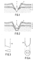
- Figure 1 is a cross-sectional view of a part of a substrate 1 which supports conductor layers 2 and 4 which are separated from each other by an insulating layer 3.
- Substrate 1 is formed from a material which is commonly used in the art, such as glass fibre-reinforced epoxy resin having a layer thickness of 1.5 mm and a glass- transition. temperature of 1250C.
- the glass fibres should preferably not be arranged in a mesh-like pattern, especially in the insulating layer 3 to allow a depression to be made independently of its location.
- the conductor layers 2 and 4 consist of, for example, 35 / um thick patterned copper layers.
- Insulating layer 3 may be of the same material as substrate 1, having a thickness of, for example, 75 / um.
- the layers can be bonded together by means of a known compression method.
- a depression 5 is formed so that conductor layer 4 is pressed beyond conductor layer 2. This results in an annular contact 6 between conductor layers 2 and 4.
- a bulge 7 is produced around depression 5 due to the accumulation, amongst others, of deformed insulation material 3.
- Bulge 7 is of small dimensions and in contrast to, for example, bent and soldered lugs, it does not hamper the further mechanical processing of the multilayer printed circuit board.
- conductors with a width of 0.5 mm a depression with a diameter of, for example, 0.2 mm is used.
- connection can be further reinforced by providing a conductive material, for example, solder, in the depression.
- a conductive material for example, solder
- Non-symmetrical depression tools are also suitable.
- Figure 3, for example, shows a triangular depression tool by means of which a trapezium- shaped depression can be formed.
- Figure 4 shows an obliquely truncated conical_depression tool by means of which an elliptical depression can be formed.
- a suitable shape of such a truncated cone is defined, for example, by an apex angle of the cone of approximately 50 0 , the end face making an angle of 70° with the axis of the cone, and the major axis of the ellipse of the end face having a length of 0.2 mm.
- the above-mentioned dimensions have to be adapted to the material selected and to the layer thicknesses.
Landscapes
- Engineering & Computer Science (AREA)
- Manufacturing & Machinery (AREA)
- Microelectronics & Electronic Packaging (AREA)
- Production Of Multi-Layered Print Wiring Board (AREA)
Applications Claiming Priority (2)
| Application Number | Priority Date | Filing Date | Title |
|---|---|---|---|
| NL8403755 | 1984-12-11 | ||
| NL8403755A NL8403755A (nl) | 1984-12-11 | 1984-12-11 | Werkwijze voor de vervaardiging van een meerlaags gedrukte bedrading met doorverbonden sporen in verschillende lagen en meerlaags gedrukte bedrading vervaardigd volgens de werkwijze. |
Publications (1)
| Publication Number | Publication Date |
|---|---|
| EP0187399A1 true EP0187399A1 (de) | 1986-07-16 |
Family
ID=19844891
Family Applications (1)
| Application Number | Title | Priority Date | Filing Date |
|---|---|---|---|
| EP85201917A Withdrawn EP0187399A1 (de) | 1984-12-11 | 1985-11-21 | Verfahren zur Herstellung einer mehrschichtigen gedruckten Schaltung in der Leiter von verschiedenen Schichten miteinander verbunden sind sowie durch dieses Verfahren hergestellte mehrschichtige gedruckte Schaltung |
Country Status (4)
| Country | Link |
|---|---|
| US (1) | US4663840A (de) |
| EP (1) | EP0187399A1 (de) |
| JP (1) | JPS61140199A (de) |
| NL (1) | NL8403755A (de) |
Cited By (2)
| Publication number | Priority date | Publication date | Assignee | Title |
|---|---|---|---|---|
| EP0421054A3 (en) * | 1989-10-05 | 1991-08-21 | International Business Machines Corporation | Method for forming a defect-free surface on a porous ceramic substrate |
| WO1999049708A1 (en) * | 1998-03-27 | 1999-09-30 | Minnesota Mining And Manufacturing Company | Method for making electrical connections between conductors separated by a dielectric |
Families Citing this family (37)
| Publication number | Priority date | Publication date | Assignee | Title |
|---|---|---|---|---|
| US5121299A (en) * | 1989-12-29 | 1992-06-09 | International Business Machines Corporation | Multi-level circuit structure utilizing conductive cores having conductive protrusions and cavities therein |
| US5146674A (en) * | 1991-07-01 | 1992-09-15 | International Business Machines Corporation | Manufacturing process of a high density substrate design |
| US6232789B1 (en) | 1997-05-28 | 2001-05-15 | Cascade Microtech, Inc. | Probe holder for low current measurements |
| US5729150A (en) * | 1995-12-01 | 1998-03-17 | Cascade Microtech, Inc. | Low-current probe card with reduced triboelectric current generating cables |
| US5736679A (en) * | 1995-12-26 | 1998-04-07 | International Business Machines Corporation | Deformable interconnect structure for connecting an internal plane to a through-hole in a multilayer circuit board |
| US5914613A (en) | 1996-08-08 | 1999-06-22 | Cascade Microtech, Inc. | Membrane probing system with local contact scrub |
| US6034533A (en) * | 1997-06-10 | 2000-03-07 | Tervo; Paul A. | Low-current pogo probe card |
| US6256882B1 (en) | 1998-07-14 | 2001-07-10 | Cascade Microtech, Inc. | Membrane probing system |
| US6578264B1 (en) | 1999-06-04 | 2003-06-17 | Cascade Microtech, Inc. | Method for constructing a membrane probe using a depression |
| AU5224499A (en) * | 1999-07-21 | 2001-02-13 | Cascade Microtech, Inc. | Membrane probing system |
| US6838890B2 (en) * | 2000-02-25 | 2005-01-04 | Cascade Microtech, Inc. | Membrane probing system |
| US6954986B2 (en) * | 2000-03-31 | 2005-10-18 | Dyconex Ag | Method for fabricating electrical connecting element |
| AU2001242204A1 (en) * | 2000-03-31 | 2001-10-23 | Dyconex Patente Ag | Method and device for fabricating electrical connecting elements, and connectingelement |
| EP1269808B1 (de) * | 2000-03-31 | 2007-08-22 | Dyconex AG | Verfahren zur herstellung elektrischer verbindungselemente und verbindungselement |
| DE10143173A1 (de) | 2000-12-04 | 2002-06-06 | Cascade Microtech Inc | Wafersonde |
| DE10101236A1 (de) * | 2001-01-12 | 2002-07-25 | Schunk Ultraschalltechnik Gmbh | Verfahren und Vorrichtung zum Verbinden von Leitern |
| WO2003052435A1 (en) | 2001-08-21 | 2003-06-26 | Cascade Microtech, Inc. | Membrane probing system |
| JP2005527823A (ja) | 2002-05-23 | 2005-09-15 | カスケード マイクロテック インコーポレイテッド | デバイスのテスト用プローブ |
| US6724205B1 (en) * | 2002-11-13 | 2004-04-20 | Cascade Microtech, Inc. | Probe for combined signals |
| US7057404B2 (en) | 2003-05-23 | 2006-06-06 | Sharp Laboratories Of America, Inc. | Shielded probe for testing a device under test |
| JP2005026322A (ja) * | 2003-06-30 | 2005-01-27 | Shinko Electric Ind Co Ltd | 配線基板及びその製造方法 |
| DE202004021093U1 (de) | 2003-12-24 | 2006-09-28 | Cascade Microtech, Inc., Beaverton | Aktiver Halbleiterscheibenmessfühler |
| US7368927B2 (en) | 2004-07-07 | 2008-05-06 | Cascade Microtech, Inc. | Probe head having a membrane suspended probe |
| KR20070058522A (ko) | 2004-09-13 | 2007-06-08 | 캐스케이드 마이크로테크 인코포레이티드 | 양측 프루빙 구조 |
| US7656172B2 (en) | 2005-01-31 | 2010-02-02 | Cascade Microtech, Inc. | System for testing semiconductors |
| US7535247B2 (en) | 2005-01-31 | 2009-05-19 | Cascade Microtech, Inc. | Interface for testing semiconductors |
| US7449899B2 (en) | 2005-06-08 | 2008-11-11 | Cascade Microtech, Inc. | Probe for high frequency signals |
| JP5080459B2 (ja) | 2005-06-13 | 2012-11-21 | カスケード マイクロテック インコーポレイテッド | 広帯域能動/受動差動信号プローブ |
| DE202007018733U1 (de) | 2006-06-09 | 2009-03-26 | Cascade Microtech, Inc., Beaverton | Messfühler für differentielle Signale mit integrierter Symmetrieschaltung |
| US7764072B2 (en) | 2006-06-12 | 2010-07-27 | Cascade Microtech, Inc. | Differential signal probing system |
| US7723999B2 (en) | 2006-06-12 | 2010-05-25 | Cascade Microtech, Inc. | Calibration structures for differential signal probing |
| US7443186B2 (en) | 2006-06-12 | 2008-10-28 | Cascade Microtech, Inc. | On-wafer test structures for differential signals |
| US7403028B2 (en) | 2006-06-12 | 2008-07-22 | Cascade Microtech, Inc. | Test structure and probe for differential signals |
| JP4840132B2 (ja) * | 2006-12-26 | 2011-12-21 | 株式会社デンソー | 多層基板の製造方法 |
| US7876114B2 (en) | 2007-08-08 | 2011-01-25 | Cascade Microtech, Inc. | Differential waveguide probe |
| US7888957B2 (en) | 2008-10-06 | 2011-02-15 | Cascade Microtech, Inc. | Probing apparatus with impedance optimized interface |
| WO2010059247A2 (en) | 2008-11-21 | 2010-05-27 | Cascade Microtech, Inc. | Replaceable coupon for a probing apparatus |
Citations (5)
| Publication number | Priority date | Publication date | Assignee | Title |
|---|---|---|---|---|
| US3346950A (en) * | 1965-06-16 | 1967-10-17 | Ibm | Method of making through-connections by controlled punctures |
| US3364300A (en) * | 1965-03-19 | 1968-01-16 | Texas Instruments Inc | Modular circuit boards |
| US3499098A (en) * | 1968-10-08 | 1970-03-03 | Bell Telephone Labor Inc | Interconnected matrix conductors and method of making the same |
| DE2347216A1 (de) * | 1973-09-19 | 1975-03-27 | Siemens Ag | Verfahren zum durchkontaktieren eines beidseitig metallkaschierten basismaterials fuer gedruckte schaltungen |
| FR2313843A1 (fr) * | 1975-06-03 | 1976-12-31 | Siemens Ag | Circuit imprime flexible, et procede pour sa fabrication |
Family Cites Families (6)
| Publication number | Priority date | Publication date | Assignee | Title |
|---|---|---|---|---|
| US3037265A (en) * | 1957-12-30 | 1962-06-05 | Ibm | Method for making printed circuits |
| GB1261039A (en) * | 1968-10-02 | 1972-01-19 | Elliott Brothers London Ltd | Improvements relating to printed circuit assemblies |
| DE2107591A1 (de) * | 1971-02-17 | 1972-08-31 | Siemens Ag | Verfahren zur Durchkontaktierung von beidseitig mit Leiterbahnen beschichteten Folien |
| US4183137A (en) * | 1977-02-15 | 1980-01-15 | Lomerson Robert B | Method for metalizing holes in insulation material |
| US4319708A (en) * | 1977-02-15 | 1982-03-16 | Lomerson Robert B | Mechanical bonding of surface conductive layers |
| SU1019682A1 (ru) * | 1982-01-29 | 1983-05-23 | Предприятие П/Я М-5181 | Способ изготовлени многослойных печатных плат |
-
1984
- 1984-12-11 NL NL8403755A patent/NL8403755A/nl not_active Application Discontinuation
-
1985
- 1985-11-21 EP EP85201917A patent/EP0187399A1/de not_active Withdrawn
- 1985-12-02 US US06/803,357 patent/US4663840A/en not_active Expired - Fee Related
- 1985-12-07 JP JP60274364A patent/JPS61140199A/ja active Pending
Patent Citations (5)
| Publication number | Priority date | Publication date | Assignee | Title |
|---|---|---|---|---|
| US3364300A (en) * | 1965-03-19 | 1968-01-16 | Texas Instruments Inc | Modular circuit boards |
| US3346950A (en) * | 1965-06-16 | 1967-10-17 | Ibm | Method of making through-connections by controlled punctures |
| US3499098A (en) * | 1968-10-08 | 1970-03-03 | Bell Telephone Labor Inc | Interconnected matrix conductors and method of making the same |
| DE2347216A1 (de) * | 1973-09-19 | 1975-03-27 | Siemens Ag | Verfahren zum durchkontaktieren eines beidseitig metallkaschierten basismaterials fuer gedruckte schaltungen |
| FR2313843A1 (fr) * | 1975-06-03 | 1976-12-31 | Siemens Ag | Circuit imprime flexible, et procede pour sa fabrication |
Cited By (2)
| Publication number | Priority date | Publication date | Assignee | Title |
|---|---|---|---|---|
| EP0421054A3 (en) * | 1989-10-05 | 1991-08-21 | International Business Machines Corporation | Method for forming a defect-free surface on a porous ceramic substrate |
| WO1999049708A1 (en) * | 1998-03-27 | 1999-09-30 | Minnesota Mining And Manufacturing Company | Method for making electrical connections between conductors separated by a dielectric |
Also Published As
| Publication number | Publication date |
|---|---|
| NL8403755A (nl) | 1986-07-01 |
| JPS61140199A (ja) | 1986-06-27 |
| US4663840A (en) | 1987-05-12 |
Similar Documents
| Publication | Publication Date | Title |
|---|---|---|
| US4663840A (en) | Method of interconnecting conductors of different layers of a multilayer printed circuit board | |
| US4804574A (en) | Laminated printed coil structure | |
| US4121044A (en) | Flexible through-contacted printed circuits | |
| EP0602609B1 (de) | Elektrischer Verbinder mit einer abgestützten gewölbten Gestaltung | |
| US20010002728A1 (en) | Printed-circuit board and method of manufacture thereof | |
| JPH07263830A (ja) | 電子パッケージ用の空洞および隆起部相互接続構造 | |
| US3977074A (en) | Double sided printed circuit board and method for making same | |
| CA2030826A1 (en) | Composite circuit board with thick embedded conductor and method of manufacturing the same | |
| US20040047136A1 (en) | Wiring board having terminal | |
| US5119272A (en) | Circuit board and method of producing circuit board | |
| JP2002523881A (ja) | 回路担体における電気的構成部材の接続のための接続装置並びにその製造法 | |
| US4925522A (en) | Printed circuit assembly with contact dot | |
| US4945190A (en) | Circuit board device for magnetics circuit and method of manufacturing same | |
| JPH0321095A (ja) | 大電流回路基板の製造方法 | |
| EP0997060A1 (de) | Eine vorrichtung und verfahren in elektronischen systemen | |
| JP2001111211A (ja) | プリント基板の製造方法およびプリント基板 | |
| JPH0373594A (ja) | 金属板ベース回路基板及びその製法 | |
| JPS6347157B2 (de) | ||
| JP2954559B2 (ja) | 配線基板の電極構造 | |
| JPH0416913B2 (de) | ||
| JPH09199242A (ja) | プリント配線板一体型コネクタ及びその製造方法 | |
| JPH1197610A (ja) | 電子部品の実装方法および電子部品 | |
| JP2534355B2 (ja) | 大電流回路基板の製造方法 | |
| JPH05218604A (ja) | 金属ベース回路基板 | |
| JPH11168272A (ja) | Hfハウジング |
Legal Events
| Date | Code | Title | Description |
|---|---|---|---|
| PUAI | Public reference made under article 153(3) epc to a published international application that has entered the european phase |
Free format text: ORIGINAL CODE: 0009012 |
|
| AK | Designated contracting states |
Kind code of ref document: A1 Designated state(s): DE FR GB NL |
|
| 17P | Request for examination filed |
Effective date: 19870114 |
|
| STAA | Information on the status of an ep patent application or granted ep patent |
Free format text: STATUS: THE APPLICATION IS DEEMED TO BE WITHDRAWN |
|
| 18D | Application deemed to be withdrawn |
Effective date: 19880531 |
|
| RIN1 | Information on inventor provided before grant (corrected) |
Inventor name: UBBENS, HENRICUS DETHMER UBBO Inventor name: LANGEVELD, PEER |