EP0188764B1 - Arrangement optique avec un miroir ou réseau concave - Google Patents
Arrangement optique avec un miroir ou réseau concave Download PDFInfo
- Publication number
- EP0188764B1 EP0188764B1 EP85116187A EP85116187A EP0188764B1 EP 0188764 B1 EP0188764 B1 EP 0188764B1 EP 85116187 A EP85116187 A EP 85116187A EP 85116187 A EP85116187 A EP 85116187A EP 0188764 B1 EP0188764 B1 EP 0188764B1
- Authority
- EP
- European Patent Office
- Prior art keywords
- grating
- optical arrangement
- arrangement according
- concave
- plane
- Prior art date
- Legal status (The legal status is an assumption and is not a legal conclusion. Google has not performed a legal analysis and makes no representation as to the accuracy of the status listed.)
- Expired - Lifetime
Links
- 230000003287 optical effect Effects 0.000 title claims description 14
- 201000009310 astigmatism Diseases 0.000 claims description 14
- 238000003384 imaging method Methods 0.000 claims description 9
- 239000000835 fiber Substances 0.000 claims description 6
- 229910003460 diamond Inorganic materials 0.000 claims description 3
- 239000010432 diamond Substances 0.000 claims description 3
- 238000012634 optical imaging Methods 0.000 claims 1
- 239000013307 optical fiber Substances 0.000 description 30
- 230000005855 radiation Effects 0.000 description 13
- 239000011521 glass Substances 0.000 description 10
- 238000005286 illumination Methods 0.000 description 9
- 239000006185 dispersion Substances 0.000 description 8
- 230000000694 effects Effects 0.000 description 6
- 238000001228 spectrum Methods 0.000 description 6
- 239000013078 crystal Substances 0.000 description 4
- 230000003595 spectral effect Effects 0.000 description 3
- 206010010071 Coma Diseases 0.000 description 2
- 230000005540 biological transmission Effects 0.000 description 2
- 230000004907 flux Effects 0.000 description 2
- 238000004519 manufacturing process Methods 0.000 description 2
- 239000000463 material Substances 0.000 description 2
- 229910052724 xenon Inorganic materials 0.000 description 2
- FHNFHKCVQCLJFQ-UHFFFAOYSA-N xenon atom Chemical compound [Xe] FHNFHKCVQCLJFQ-UHFFFAOYSA-N 0.000 description 2
- 230000006978 adaptation Effects 0.000 description 1
- 230000015572 biosynthetic process Effects 0.000 description 1
- 238000010276 construction Methods 0.000 description 1
- 238000005516 engineering process Methods 0.000 description 1
- 238000003702 image correction Methods 0.000 description 1
- 238000005342 ion exchange Methods 0.000 description 1
- 238000005468 ion implantation Methods 0.000 description 1
- 238000000034 method Methods 0.000 description 1
Images


Classifications
-
- G—PHYSICS
- G01—MEASURING; TESTING
- G01J—MEASUREMENT OF INTENSITY, VELOCITY, SPECTRAL CONTENT, POLARISATION, PHASE OR PULSE CHARACTERISTICS OF INFRARED, VISIBLE OR ULTRAVIOLET LIGHT; COLORIMETRY; RADIATION PYROMETRY
- G01J3/00—Spectrometry; Spectrophotometry; Monochromators; Measuring colours
- G01J3/12—Generating the spectrum; Monochromators
- G01J3/18—Generating the spectrum; Monochromators using diffraction elements, e.g. grating
- G01J3/20—Rowland circle spectrometers
-
- G—PHYSICS
- G01—MEASURING; TESTING
- G01J—MEASUREMENT OF INTENSITY, VELOCITY, SPECTRAL CONTENT, POLARISATION, PHASE OR PULSE CHARACTERISTICS OF INFRARED, VISIBLE OR ULTRAVIOLET LIGHT; COLORIMETRY; RADIATION PYROMETRY
- G01J3/00—Spectrometry; Spectrophotometry; Monochromators; Measuring colours
- G01J3/02—Details
- G01J3/0256—Compact construction
- G01J3/0259—Monolithic
-
- G—PHYSICS
- G01—MEASURING; TESTING
- G01J—MEASUREMENT OF INTENSITY, VELOCITY, SPECTRAL CONTENT, POLARISATION, PHASE OR PULSE CHARACTERISTICS OF INFRARED, VISIBLE OR ULTRAVIOLET LIGHT; COLORIMETRY; RADIATION PYROMETRY
- G01J3/00—Spectrometry; Spectrophotometry; Monochromators; Measuring colours
- G01J3/12—Generating the spectrum; Monochromators
- G01J3/18—Generating the spectrum; Monochromators using diffraction elements, e.g. grating
-
- G—PHYSICS
- G02—OPTICS
- G02B—OPTICAL ELEMENTS, SYSTEMS OR APPARATUS
- G02B6/00—Light guides; Structural details of arrangements comprising light guides and other optical elements, e.g. couplings
- G02B6/24—Coupling light guides
- G02B6/26—Optical coupling means
- G02B6/28—Optical coupling means having data bus means, i.e. plural waveguides interconnected and providing an inherently bidirectional system by mixing and splitting signals
- G02B6/293—Optical coupling means having data bus means, i.e. plural waveguides interconnected and providing an inherently bidirectional system by mixing and splitting signals with wavelength selective means
- G02B6/29304—Optical coupling means having data bus means, i.e. plural waveguides interconnected and providing an inherently bidirectional system by mixing and splitting signals with wavelength selective means operating by diffraction, e.g. grating
- G02B6/29305—Optical coupling means having data bus means, i.e. plural waveguides interconnected and providing an inherently bidirectional system by mixing and splitting signals with wavelength selective means operating by diffraction, e.g. grating as bulk element, i.e. free space arrangement external to a light guide
- G02B6/29307—Optical coupling means having data bus means, i.e. plural waveguides interconnected and providing an inherently bidirectional system by mixing and splitting signals with wavelength selective means operating by diffraction, e.g. grating as bulk element, i.e. free space arrangement external to a light guide components assembled in or forming a solid transparent unitary block, e.g. for facilitating component alignment
-
- G—PHYSICS
- G02—OPTICS
- G02B—OPTICAL ELEMENTS, SYSTEMS OR APPARATUS
- G02B6/00—Light guides; Structural details of arrangements comprising light guides and other optical elements, e.g. couplings
- G02B6/24—Coupling light guides
- G02B6/26—Optical coupling means
- G02B6/28—Optical coupling means having data bus means, i.e. plural waveguides interconnected and providing an inherently bidirectional system by mixing and splitting signals
- G02B6/293—Optical coupling means having data bus means, i.e. plural waveguides interconnected and providing an inherently bidirectional system by mixing and splitting signals with wavelength selective means
- G02B6/29304—Optical coupling means having data bus means, i.e. plural waveguides interconnected and providing an inherently bidirectional system by mixing and splitting signals with wavelength selective means operating by diffraction, e.g. grating
- G02B6/29305—Optical coupling means having data bus means, i.e. plural waveguides interconnected and providing an inherently bidirectional system by mixing and splitting signals with wavelength selective means operating by diffraction, e.g. grating as bulk element, i.e. free space arrangement external to a light guide
- G02B6/2931—Diffractive element operating in reflection
-
- G—PHYSICS
- G02—OPTICS
- G02B—OPTICAL ELEMENTS, SYSTEMS OR APPARATUS
- G02B6/00—Light guides; Structural details of arrangements comprising light guides and other optical elements, e.g. couplings
- G02B6/24—Coupling light guides
- G02B6/42—Coupling light guides with opto-electronic elements
- G02B6/4201—Packages, e.g. shape, construction, internal or external details
- G02B6/4204—Packages, e.g. shape, construction, internal or external details the coupling comprising intermediate optical elements, e.g. lenses, holograms
- G02B6/4215—Packages, e.g. shape, construction, internal or external details the coupling comprising intermediate optical elements, e.g. lenses, holograms the intermediate optical elements being wavelength selective optical elements, e.g. variable wavelength optical modules or wavelength lockers
-
- G—PHYSICS
- G01—MEASURING; TESTING
- G01J—MEASUREMENT OF INTENSITY, VELOCITY, SPECTRAL CONTENT, POLARISATION, PHASE OR PULSE CHARACTERISTICS OF INFRARED, VISIBLE OR ULTRAVIOLET LIGHT; COLORIMETRY; RADIATION PYROMETRY
- G01J3/00—Spectrometry; Spectrophotometry; Monochromators; Measuring colours
- G01J3/02—Details
- G01J3/0205—Optical elements not provided otherwise, e.g. optical manifolds, diffusers, windows
-
- G—PHYSICS
- G01—MEASURING; TESTING
- G01J—MEASUREMENT OF INTENSITY, VELOCITY, SPECTRAL CONTENT, POLARISATION, PHASE OR PULSE CHARACTERISTICS OF INFRARED, VISIBLE OR ULTRAVIOLET LIGHT; COLORIMETRY; RADIATION PYROMETRY
- G01J3/00—Spectrometry; Spectrophotometry; Monochromators; Measuring colours
- G01J3/02—Details
- G01J3/0256—Compact construction
Definitions
- the present invention relates to an optical arrangement for imaging the entry or exit surfaces of optical fibers or spectrometer columns.
- a preferred field of application of the invention is spectrometers, including the illumination device, and multiplexers and demultiplexers for fiber-optic information transmission.
- Spherical concave mirrors show an astigmatism that increases with the angle of incidence when the angle of incidence is different from zero. This can be corrected by using toric or elliptical mirrors; such mirrors are complex to manufacture and therefore expensive.
- Spherical concave gratings also show this astigmatism because their imaging properties are naturally similar to those of spherical concave mirrors.
- good possibilities for correcting astigmatism are known by suitable choice of the source points (see, for example, R. Bittner, Optik 64 , 185 (1983)), but conventional gratings can have a higher efficiency due to their blaze angle in the visible and infrared spectral range that they are still very important today.
- the definition of the source points for image error correction in the geometrical arrangement of the grating, entrance slit and spectral plane is very narrow, so that a further degree of freedom for correction possibilities would be advantageous.
- Wavelength multiplexers and demultiplexers with concave gratings and layered waveguides are known from US 4,274,706 and EP 0 121 812.
- the entire space between the object plane, the grating and the image plane is filled by the layer waveguide, in the EP document it connects to the grating and light guide compensating pieces are provided for adaptation to input and output optical fibers.
- the grating is only illuminated as a narrow strip, which has the height of the layer waveguide in the furrow direction. Astigmatism is therefore not a problem.
- an obliquely illuminated spherical mirror is introduced to produce an astigmatic image of the light source on the entrance and exit surface of the crystal.
- the astigmatic properties of crystal and mirror compensate each other. No reference is made to other types of applications.
- the present invention is therefore based on the object of specifying the simplest possible correction option for the astigmatism of concave mirrors and concave gratings, or to obtain a further degree of freedom for correction possibilities in the case of holographically produced concave gratings.
- the reflecting surfaces of the layer waveguide are curved.
- the formation of the reflecting surfaces as concentric spherical surfaces is particularly advantageous.
- An advantageous embodiment of the invention is characterized by an illumination device with a concave mirror and an illumination source. With such an arrangement, a large radiation flow from the illumination source e.g. insert into an optical fiber.
- wavelength multiplexers and demultiplexers with a concave grating in which the supply and discharge of the radiation e.g. done by optical fibers.
- the concave grating is constructed in a known manner from at least two areas which are divided with differently shaped diamond styluses. In this way, good energy ratios can be achieved over a wide wavelength range.
- the combination with a second arrangement with a concave mirror or concave grating is particularly advantageous, a common layer waveguide being used for both arrangements.
- 11 denotes a light source, for example a xenon lamp, which is imaged by the concave mirror 12 into the optical fiber 15 via the deflecting mirror 13.
- the layer waveguide 14 is arranged in front of the entry surface 15a of the optical fiber 15. Its wave-guiding layer 14b is cuboid and has a width 14a in the plane of the drawing which is equal to the core diameter 15b of the optical fiber 15.
- the layer waveguide has a height perpendicular to the plane of the drawing which is a multiple of the diameter of the core 15b of the optical fiber 15. The exact value of the height is not critical if a minimum value is observed.
- the wave-guiding layer 14b of the layer waveguide 14 expediently sits on a carrier plate 14c and is covered with a second plate 14d, both plates having a lower refractive index than the wave-guiding layer 14b.
- the refractive index of the waveguiding Layer is expediently chosen to be at least approximately equal to the refractive index of core 15b of optical fiber 15.
- the wave-guiding layer 14b Due to the physical mode of operation of the wave-guiding layer 14b, it is of course also possible to limit the wave-guiding layer 14b by air instead of one or both plates 14c and 14d. In the case of the optical fiber 15, the jacket 15c can likewise be replaced by air.
- the effect of the layered waveguide 14 is shown in the following numerical example: radius of the concave mirror 12: 100 mm, i.e. Focal length 50 mm; Diameter of the concave mirror 12: 40 mm; Deflection angle 12a of the concave mirror: 19 °.
- radius of the concave mirror 12 100 mm, i.e. Focal length 50 mm
- Diameter of the concave mirror 12 40 mm
- Deflection angle 12a of the concave mirror 19 °.
- a point-shaped light source 11 in the image plane 13a would result in a scattering figure with an extension of approximately 2.3 mm perpendicular to the drawing plane and with a projection of approximately 65 ⁇ m into the drawing plane.
- this figure of dispersion in the entry surface 15a of the optical fiber 15 is reduced to approximately 56 ⁇ m perpendicular to the drawing plane and in the drawing plane in accordance with the layer waveguide thickness 14b; i.e. with a core diameter 15b of e.g. 50 .mu.m of the optical fiber 15 and a xenon lamp as the light source through the layer waveguide 14 a radiation flux that is 30 times larger enters the optical fiber 15 than without the layer waveguide.
- the layer waveguide must have a height of at least 2.3 mm.
- the layered waveguide - as the numerical example shows - is relatively thin and would therefore be difficult to manufacture as an individual part, it is expedient to produce it in the following manner, for example:
- the glass for the layered waveguide is turned onto the optically polished surface of the carrier plate 14c but still easy to handle plate, which also has an optically polished surface, cemented or blown open. Then the cemented or blown open The plate is sanded and polished until it has the desired thickness for the waveguiding layer.
- the cover plate 14d is then optionally cemented or blown onto this surface.
- the method of ion implantation or ion exchange which has become known recently, can also be used to produce the wave-guiding layer, with which the refractive index in glasses can be changed in a defined manner and with a defined thickness on the surface (see, for example, Lilienhof ea Optics Communications 35 , 49 (1980)).
- FIG. 2 shows a diode line spectrometer with an optical fiber 25, of which only the core is drawn and the end face 25a of which serves as an entry slit for the spectrometer. Attached to the end face is the layered waveguide 24, of which only the wave-guiding layer is also drawn and which also has a width in the plane of the drawing which is equal to the core diameter 25a of the optical fiber 25.
- a concave grating 22 serves as the dispersing element and a diode row 21 is used as the receiver.
- Concave grating 22, diode row 21 and entry gap 25a, or the end face 24a of the layer waveguide 24 lie in a known manner on the Rowland circle 26.
- the following numerical example shows the effect of the layer waveguide 24: radius of the concave grating 22: 200 mm, ie diameter of the Rowland circle 26: 200 mm; Kankav grid diameter 80 mm; Inlet opening 27: 1: 2.5; Angle of incidence 28: 5.16 °; Furrow density of the concave grating 150 lines / mm; Wavelength range 400-800 nm; Spectra length on the receiver 21: 12 mm.
- a point in the plane of the entry slit 25a if this lies on the Rowland circle 26) on the receiver surface 21 would result in a scattering figure which has a dimension of 0.63 mm in the furrow direction (ie perpendicular to the plane of the drawing).
- This value is reduced to 4.3 ⁇ m by the layered waveguide 24 made of SF 10 with a length of 2.74 mm. Since common diode lines have an extension of 25 ⁇ m in the furrow direction, the receiver receives a radiation flux that is 20 times larger due to the layer waveguide 24.
- the dispersion figure of maximum 36 ⁇ m (mathematically) is folded in the direction of dispersion with the thickness of the layer waveguide; ie it can be kept below the resolution limit of common diode rows.
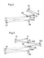
- FIG. 3 shows a complete diode line spectrometer with an illumination device and a cuvette.
- the lighting device corresponds to that shown in FIG. 1, only the light source 11 being imaged in the plane 34a, which lies close to the cuvette 35.
- the layer waveguide 34 is arranged before and after the plane 34a. With the part of the layer waveguide 34 (seen in the direction of light) arranged in front of the plane 34a, the imaging correction for the lighting part takes place; The image correction for the following spectrometer part, which consists of the concave grating 37 and the diode row 38, takes place with the part of the layer waveguide 34 arranged after the plane 34a. In this way it is achieved that two imaging systems are corrected with one layer waveguide.
- FIG. 4 shows a modified embodiment of the lighting device.
- the image of the light source 11 imaged by the first concave mirror 12 in the plane 44a is imaged by the second concave mirror 12a in the plane 46a directly behind the cuvette 45.
- a common layer waveguide 44 is used for both imaging systems of the illumination device.
- the layer waveguide 46 which is attached to the plane 46a, is provided to correct the astigmatism.
- the cuvette 45 is located directly in front of this plane, the light bundle therefore has the same extent for a punctiform light source 11 in the cuvette 45 perpendicular to the drawing plane as in the drawing plane.
- FIG. 5 shows a spectrometer with an entry slit 51 and a plurality of exit slits 53a, 53b, 53c as an example of a layer waveguide with curved reflecting surfaces.
- the concave grating 52 and the exit gaps 53a, 53b, 53c again lie on the Rawland circle 56.
- the entry gap 51 would normally also lie on the Rowland circle 56.
- the end 54e of the layered waveguide lies on the Rowland circle 56 and the entry slit 51 is located directly in front of the beginning 54a of the layered waveguide 54 lies in the middle of the spectrum used. In this way, in addition to correcting the astigmatism, a correction of the sagittal coma is achieved.
- the effect of the layer waveguide 54 is illustrated by the following numerical example: radius of the concave grating 52: 200 mm, i.e. Rowland circle diameter 56: 200 mm; Diameter of the concave grating 40 mm; Inlet opening 57: 1: 5; Angle of incidence 58: 21.1 °; Furrow density of the concave grating 600 lines / mm; Wavelength range 400-800 nm; Spectra length on the Rowland circle 56: 48 mm.
- layer waveguide 54 Without layer waveguide 54, a point in the plane of the entrance slit 51 (if this lies on the Rowland circle 56) in the plane e of the columns 53a, 53b, 53c would result in a scattering figure which has a dimension of 5 in the furrow direction (ie perpendicular to the plane of the drawing). 56 mm. This value is reduced to 93 ⁇ m by a cuboidal layer waveguide made of PSK 3 with a length of 43.09 mm.
- the thickness of the layer waveguide is expediently chosen to be the same as the width of the entrance slit, e.g. 10 ⁇ m.
- 62 denotes a holographic concave grating, onto which the radiation coming from the entrance slit 61 strikes at an angle 65 of 15.5 ° with respect to the grating normal with the large entrance opening of 1: 2.5.
- the radiation reflected by the concave grating 62 has an angle 66 of 24 ° to the grating normal for the center of the wavelength range from 360 to 780 nm, the spectrum in the plane 63 having a length of 3.2 mm.
- the deflection angle 67 is 39.5 °; it is therefore much larger than the largest deflection angle of 20 °, which can be achieved for holographic gratings with known astigmatism correction.
- the effect of the layer waveguide 64 for the deflection angle of 39.5 ° shown in FIG. 6 is shown in the following numerical example: concave grating radius 29.078 mm; Concave grid diameter 11.1 mm; average groove density of the concave grating 246.5 lines / mm; Input focal length 27.77 mm; Initial focal length 27.77 mm.
- the layered waveguide 64 made of SF 10 with a length of 6.9 mm reduces the scattering figure in the spectral plane 63 perpendicular to the drawing plane from 1.4 mm to 28 ⁇ m for a point in the plane of the gap 61; in the direction of dispersion, a maximum figure of 75 ⁇ m is obtained.
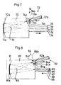
- FIG. 7 shows a demultiplexer for the fiber optic information transmission as a further exemplary embodiment.
- Such demultiplexers today often consist of a glass or plastic body in favor of a compact and robust design, which contains the necessary optical components or to which they are cemented. If normal concave grids are used in favor of the simplest possible construction, the optical properties due to the astigmatism of the concave grating are unsatisfactory.
- 70 denotes a glass or plastic body on the convex surface 70a of the concave grating 71a using known technology was copied and provided with a mirror layer.
- the radiation to be split is fed to the demultiplexer via the optical fiber 72, the core 72b of which has a diameter of 50 ⁇ m, for example.
- a layered waveguide 74 is arranged between the end 72a of the optical fiber 72 and the glass or plastic body 70, the waveguiding layer 74b of which has the same thickness 74a in the plane of the drawing as the core 72b of the optical fiber.
- the parallelepiped-shaped wave-guiding layer 74b has a substantially greater extent, which is not critical if a minimum value is observed.
- the wave-guiding layer 74b is made of SF 10, for example, and sits between the glass plots 74c and 74d made of F 2.
- the radiation coming from the optical fiber 72 passes through the layer waveguide 74 onto the concave grating 71a and is broken down by the latter into the individual wavelengths which are taken up by the optical fibers 75 to 79.
- the latter have a core diameter of e.g. 200 ⁇ m, so that small shifts in the wavelengths (e.g. due to the tolerances of the transmitter diodes) and small tolerances of the entire structure of the demultiplexer are compensated for.
- the following numerical example shows the effect of the layered waveguide 74: material of the glass body 70: SF 10; Concave grating radius 63.551 mm; Grating diameter 17.3 mm; Groove density 248 lines / mm; Linear dispersion 107.64 nm / mm; Input focal length 62.3 mm; Starting focal length 63.5 mm; Angle of incidence 73: 11.38 °; Wavelength range 1100 to 1600 nm with 17 channels.
- the layered waveguide 74 with a length of 2.52 mm and a height of at least 0.74 mm reduces the figure of dispersion with an extension of 0.69 mm in the furrow direction to 13 ⁇ m. As a result, a radiation flow that is larger by a factor of 3.7 reaches the output optical fibers.
- the concave grating 71a consists in a known manner (see, for example, MC Hutley, Diffraction Gratings, London 1982), for example, from three adjacent areas which are divided with differently shaped diamond styluses, so that the change in the block wavelength caused by the curvature of the concave grating is reduced to 1/3.
- the concave grating 81a is copied onto a separate part 81 and, together with it, is cemented onto the glass or plastic body 80.
- the concave grating images all of the radiations arriving through the input optical fibers 85 to 89 with different wavelength ranges into the output fiber 82.
- the layered waveguide 84 sits between the glass or plastic body 80 and the output optical fiber 82. This already brings about a substantial improvement in the imaging properties of the concave grating when the waveguiding layer is of a cuboid shape.
- the reflecting surfaces 84e and 84f of the layer waveguide 84b are wedge-shaped to one another, the distance 84a of these surfaces at the end of the layer waveguide being equal to the core diameter 82a of the output optical fiber 82.
- This wedge-shaped design of the reflecting surfaces can not only compensate for tolerances in the dimensions of all optical parts, but also tolerances in the wavelength ranges of the individual radiations supplied by the input optical fibers, without increasing the core diameter of the output optical fiber by the usual or advantageous dimension.
- a cuboidal layered waveguide made of SF 10 with a length of 1.091 mm and a minimum height of 0.25 mm reduces the scattering figure in the furrow direction from 0.2 mm to 0.6 ⁇ m.
- the conical design of the layer waveguide 84 with a width of 50 ⁇ m on the fiber side 84a and 100 ⁇ m on the grating side 84g increases the wavelength tolerance per channel from 6.8 nm to 15.9 nm.
Landscapes
- Physics & Mathematics (AREA)
- Spectroscopy & Molecular Physics (AREA)
- General Physics & Mathematics (AREA)
- Optics & Photonics (AREA)
- Spectrometry And Color Measurement (AREA)
- Investigating Or Analysing Materials By Optical Means (AREA)
- Optical Couplings Of Light Guides (AREA)
- Diffracting Gratings Or Hologram Optical Elements (AREA)
- Optical Integrated Circuits (AREA)
Claims (10)
- Dispositif optique de reproduction pour la formation de l'image de l'extrémité d'une fibre optique (15, 25) ou de la fente d'un spectromètre (61), comprenant un élément de reproduction sous la forme d'un miroir concave (12) ou d'un réseau concave (71a, 81a), dans le plan d'image ou dans le plan objet duquel est disposée l'extrémité de la fibre optique ou la fente du spectromètre,
caractérisé par
un élément de correction de l'astigmatisme, constitué d'un tronçon de guide d'ondes à couche dont une face d'extrémité est disposée au droit de l'image dans le plan d'image ou au droit de l'objet dans le plan objet et dont la longueur est inférieure à la distance entre le plan d'image ou le plan objet d'une part et le miroir concave (12) ou le réseau concave (71a, 81a) d'autre part. - Dispositif optique selon la revendication 1, caractérisé en ce que le guide d'ondes à couche (54) possède des surfaces réfléchissantes courbes (54c, 54d).
- Dispositif optique selon la revendication 2, caractérisé en ce que les surfaces réfléchissantes (54c, 54b) du guide d'ondes à couche (54) sont des surfaces sphériques concentriques.
- Dispositif optique selon la revendication 1 ou 2, caractérisé en ce que les surfaces réfléchissantes (84e, 84f) du guide d'ondes à couche (84) sont disposées en coin l'une par rapport à l'autre.
- Dispositif optique selon la revendication 1 ou 4, caractérisé par sa réalisation comme un dispositif d'éclairage (figure 1) comportant un miroir concave (12) et une source d'éclairage (11).
- Dispositif optique selon une des revendications 1 à 3, caractérisé par sa réalisation comme un spectromètre (figures 2 à 6) comportant un réseau concave (22, 37, 52, 62).
- Dispositif optique selon une des revendications 1 à 4, caractérisé par sa réalisation comme un multiplexeur de longueurs d'onde (figure 4) ou comme un démultiplexeur de longueurs d'onde (figure 7) comportant un réseau concave (71a, 81a).
- Dispositif optique selon la revendication 6 ou 7, caractérisé en ce que le réseau concave (par exemple 22, 71a) est composé d'au moins deux zones divisées au moyen de burins diamantés de formes différentes.
- Dispositif optique selon une des revendications 1 à 6, caractérisé en ce qu'un second dispositif (figures 3, 4) comportant un miroir concave ou un réseau concave y est raccordé et qu'un guide d'ondes à couche commun (34, 44) est prévu pour les deux dispositifs.
- Dispositif optique selon une des revendications 1 à 9, caractérisé en ce que les indices de réfraction de la couche guide d'ondes (14b, 22, 74b) du guide d'ondes à couche et du coeur (15b, 25, 72b) d'une fibre optique qui y est accolée sont au moins approximativement égaux.
Applications Claiming Priority (2)
| Application Number | Priority Date | Filing Date | Title |
|---|---|---|---|
| DE3446726 | 1984-12-21 | ||
| DE19843446726 DE3446726A1 (de) | 1984-12-21 | 1984-12-21 | Optische anordnung mit einem konkavspiegel oder konkavgitter |
Publications (3)
| Publication Number | Publication Date |
|---|---|
| EP0188764A2 EP0188764A2 (fr) | 1986-07-30 |
| EP0188764A3 EP0188764A3 (en) | 1988-07-13 |
| EP0188764B1 true EP0188764B1 (fr) | 1993-02-03 |
Family
ID=6253445
Family Applications (1)
| Application Number | Title | Priority Date | Filing Date |
|---|---|---|---|
| EP85116187A Expired - Lifetime EP0188764B1 (fr) | 1984-12-21 | 1985-12-18 | Arrangement optique avec un miroir ou réseau concave |
Country Status (5)
| Country | Link |
|---|---|
| US (1) | US4707056A (fr) |
| EP (1) | EP0188764B1 (fr) |
| JP (1) | JPS61156004A (fr) |
| CA (1) | CA1255945A (fr) |
| DE (2) | DE3446726A1 (fr) |
Families Citing this family (39)
| Publication number | Priority date | Publication date | Assignee | Title |
|---|---|---|---|---|
| US4926412A (en) * | 1988-02-22 | 1990-05-15 | Physical Optics Corporation | High channel density wavelength division multiplexer with defined diffracting means positioning |
| DE4038638A1 (de) | 1990-12-04 | 1992-06-11 | Zeiss Carl Fa | Diodenzeilen-spektrometer |
| US5257338A (en) * | 1992-05-22 | 1993-10-26 | Biomedical Sensors, Ltd. | Device for transmitting and returning light and apparatus and method of manufacture |
| US5452085A (en) * | 1993-01-27 | 1995-09-19 | Acton Research Corporation | Spectrographic astigmatism correction system |
| US5416624A (en) * | 1993-05-17 | 1995-05-16 | Siemens Aktiengesellschaft | Bidirectional optical transmission and reception arrangement |
| DE19508100B4 (de) * | 1995-02-03 | 2004-09-02 | Storz Endoskop Gmbh | Vorrichtung zum Einkoppeln von Lichtstrahlen in eine Lichtleitfaser |
| US5675675A (en) * | 1995-12-29 | 1997-10-07 | Corning Incorporated | Bandwidth-adjusted wavelength demultiplexer |
| DE19523140A1 (de) * | 1995-06-28 | 1997-01-02 | Spectro Analytical Instr | Mehrkanal-Spektrometer mit Zeilensensor |
| EP0816877A1 (fr) * | 1996-07-01 | 1998-01-07 | Corning Incorporated | Multiplexeur/démultiplexeur avec réponse spectrale aplatie |
| JPH1062248A (ja) * | 1996-08-22 | 1998-03-06 | Hitachi Ltd | 凹面回折分光器 |
| US5926272A (en) * | 1997-04-08 | 1999-07-20 | Curtiss; Lawrence E. | Spectroscopy |
| US6298182B1 (en) * | 1997-12-13 | 2001-10-02 | Light Chip, Inc. | Wavelength division multiplexing/demultiplexing devices using polymer lenses |
| US6125223A (en) * | 1998-08-31 | 2000-09-26 | Oriel Corporation | Spectrally resolved light |
| JP3699852B2 (ja) * | 1999-02-17 | 2005-09-28 | シャープ株式会社 | 双方向光通信器および双方向光通信装置 |
| US6434299B1 (en) * | 1999-06-01 | 2002-08-13 | Lightchip, Inc. | Wavelength division multiplexing/demultiplexing devices having concave diffraction gratings |
| US6370837B1 (en) | 1999-08-04 | 2002-04-16 | Anthony B. Mcmahon | System for laying masonry blocks |
| US6650413B2 (en) * | 1999-08-08 | 2003-11-18 | Institut National D'optique | Linear spectrometer |
| US6498872B2 (en) * | 2000-02-17 | 2002-12-24 | Jds Uniphase Inc. | Optical configuration for a dynamic gain equalizer and a configurable add/drop multiplexer |
| US6925256B1 (en) | 2000-02-18 | 2005-08-02 | Diplex | Optical discriminator for transmitting and receiving in both optical fiber and free space applications |
| US6534768B1 (en) * | 2000-10-30 | 2003-03-18 | Euro-Oeltique, S.A. | Hemispherical detector |
| US6678445B2 (en) | 2000-12-04 | 2004-01-13 | Jds Uniphase Corporation | Dynamic gain flattening filter |
| US6826424B1 (en) * | 2000-12-19 | 2004-11-30 | Haishan Zeng | Methods and apparatus for fluorescence and reflectance imaging and spectroscopy and for contemporaneous measurements of electromagnetic radiation with multiple measuring devices |
| US6625346B2 (en) | 2001-03-19 | 2003-09-23 | Capella Photonics, Inc. | Reconfigurable optical add-drop multiplexers with servo control and dynamic spectral power management capabilities |
| EP1298467B1 (fr) * | 2001-09-10 | 2004-12-29 | JDS Uniphase, Inc | Interrupteur optique sélectif en longueur d'onde sans distortion des canaux non bloqués |
| US20030156819A1 (en) * | 2002-02-15 | 2003-08-21 | Mark Pruss | Optical waveguide |
| JP4221965B2 (ja) * | 2002-07-22 | 2009-02-12 | 日立電線株式会社 | 回折格子、波長合分波器及びこれらを用いた波長多重信号光伝送モジュール |
| US7068885B2 (en) * | 2004-03-24 | 2006-06-27 | Enablence, Inc. | Double diffraction grating planar lightwave circuit |
| JP2006285222A (ja) * | 2005-03-09 | 2006-10-19 | Konica Minolta Holdings Inc | 回折光学素子及び光通信モジュール |
| JP4816258B2 (ja) * | 2006-05-31 | 2011-11-16 | コニカミノルタホールディングス株式会社 | 表面反射回折格子を備えた光学装置 |
| US8738107B2 (en) | 2007-05-10 | 2014-05-27 | Medtronic Minimed, Inc. | Equilibrium non-consuming fluorescence sensor for real time intravascular glucose measurement |
| CA2677009A1 (fr) | 2007-02-06 | 2008-08-14 | Glumetrics, Inc. | Systemes et procedes optiques pour la mesure ratiometrique de la concentration en glucose dans le sang |
| US7889991B2 (en) * | 2007-02-12 | 2011-02-15 | Jds Uniphase Corporation | Planar lightwave circuit based tunable 3 port filter |
| EP2217316A4 (fr) | 2007-11-21 | 2013-01-16 | Glumetrics Inc | Utilisation d'un capteur intravasculaire à l'équilibre pour parvenir à une maîtrise précise de la glycémie |
| WO2009129186A2 (fr) | 2008-04-17 | 2009-10-22 | Glumetrics, Inc. | Capteur pour déploiement intra-vasculaire percutané sans canule à demeure |
| JP5424957B2 (ja) | 2009-04-30 | 2014-02-26 | キヤノン株式会社 | 分光測色装置およびそれを用いた画像形成装置 |
| JP2013506503A (ja) | 2009-09-30 | 2013-02-28 | グルメトリクス, インコーポレイテッド | 抗血栓性コーティングを備えたセンサー |
| US8467843B2 (en) | 2009-11-04 | 2013-06-18 | Glumetrics, Inc. | Optical sensor configuration for ratiometric correction of blood glucose measurement |
| JP2013181926A (ja) * | 2012-03-02 | 2013-09-12 | Sony Corp | 分光光学系及び分光測定装置 |
| EP3385685A1 (fr) * | 2017-04-06 | 2018-10-10 | ASML Netherlands B.V. | Système de réception de rayonnement |
Family Cites Families (12)
| Publication number | Priority date | Publication date | Assignee | Title |
|---|---|---|---|---|
| GB763556A (en) * | 1953-11-17 | 1956-12-12 | Commw Scient Ind Res Org | Improved method of and apparatus for spectrochemical analysis |
| US3664743A (en) * | 1968-11-04 | 1972-05-23 | Hitachi Ltd | Spectrophotometer |
| US3617109A (en) * | 1969-09-23 | 1971-11-02 | Bell Telephone Labor Inc | Light guide coupling and scanning arrangement |
| DE2205728C3 (de) * | 1972-02-08 | 1979-01-04 | Licentia Patent-Verwaltungs-Gmbh, 6000 Frankfurt | Aus einem mehrschichtigen Halbleiterkörper bestehendes optisches Bauelement |
| US4175864A (en) * | 1978-02-21 | 1979-11-27 | The Foxboro Company | Astigmatic illuminating system in an internal reflection spectometer |
| JPS556320A (en) * | 1978-06-27 | 1980-01-17 | Ritsuo Hasumi | Spectral module |
| US4274706A (en) * | 1979-08-30 | 1981-06-23 | Hughes Aircraft Company | Wavelength multiplexer/demultiplexer for optical circuits |
| JPS5822725B2 (ja) * | 1979-10-22 | 1983-05-11 | 日本電信電話株式会社 | 光分波器 |
| JPS56155901A (en) * | 1980-05-06 | 1981-12-02 | Nippon Telegr & Teleph Corp <Ntt> | Optical wave coupling and branching filter |
| US4387955A (en) * | 1981-02-03 | 1983-06-14 | The United States Of America As Represented By The Secretary Of The Air Force | Holographic reflective grating multiplexer/demultiplexer |
| HU187188B (en) * | 1982-11-25 | 1985-11-28 | Koezponti Elelmiszeripari | Device for generating radiation of controllable spectral structure |
| DE3309349A1 (de) * | 1983-03-16 | 1984-09-20 | Fa. Carl Zeiss, 7920 Heidenheim | Wellenlaengen-multiplexer oder -demultiplexer |
-
1984
- 1984-12-21 DE DE19843446726 patent/DE3446726A1/de not_active Withdrawn
-
1985
- 1985-12-12 US US06/808,291 patent/US4707056A/en not_active Expired - Fee Related
- 1985-12-18 CA CA000498009A patent/CA1255945A/fr not_active Expired
- 1985-12-18 DE DE8585116187T patent/DE3587071D1/de not_active Expired - Fee Related
- 1985-12-18 EP EP85116187A patent/EP0188764B1/fr not_active Expired - Lifetime
- 1985-12-20 JP JP60285923A patent/JPS61156004A/ja active Pending
Also Published As
| Publication number | Publication date |
|---|---|
| EP0188764A2 (fr) | 1986-07-30 |
| CA1255945A (fr) | 1989-06-20 |
| DE3446726A1 (de) | 1986-06-26 |
| JPS61156004A (ja) | 1986-07-15 |
| US4707056A (en) | 1987-11-17 |
| EP0188764A3 (en) | 1988-07-13 |
| DE3587071D1 (de) | 1993-03-18 |
Similar Documents
| Publication | Publication Date | Title |
|---|---|---|
| EP0188764B1 (fr) | Arrangement optique avec un miroir ou réseau concave | |
| EP0735397B1 (fr) | Dispositif micro-optique pour transformer des faisceaux d'un arrangement de diodes laser et procédé de fabrication d'un tel dispositif | |
| EP0970395B1 (fr) | Microlentilles integrees a des fibres et coupleurs optiques a reseau de bragg situe dans la fibre; spectrometres et multiplexeurs ainsi constitues | |
| DE3012184C2 (fr) | ||
| DE69823808T2 (de) | Abbildungs-spektrometer | |
| EP0942267B1 (fr) | Spectromètre | |
| EP0048379B1 (fr) | Structure de réseau de Bragg d'un guide d'ondes planaire et son application | |
| EP0194612A2 (fr) | Multiplexeur ou démultiplexeur de longueurs d'ondes | |
| DE69112906T2 (de) | Strahlteilervorrichtung mit einstellbarer Brennweite und Lage des Bildes. | |
| DE3213839A1 (de) | Optische wellenlaengen-multiplex- bzw. -demultiplexanordnung | |
| DE60114124T2 (de) | Wellenlängenkompensierter optischer wellenlängenmultiplex-koppler und zugehörige verfahren | |
| EP0212438A2 (fr) | Réseau de diffraction à réflexion ayant un haut coefficient de réflexion | |
| DE2840493A1 (de) | Frequenzselektives optisches lichtverteilerelement und verfahren zu seiner herstellung | |
| DE3122781A1 (de) | "wellenlaengenmultiplexer bzw. wellenlaengendemultiplexer" | |
| DE10054372B4 (de) | Baugruppe zum Multiplexen und/oder Demultiplexen optischer Signale | |
| WO2003012505A1 (fr) | Dispositif et procede pour multiplexer et/ou demultiplexer des signaux optiques de plusieurs longueurs d'onde | |
| DE10225176C1 (de) | Vorrichtung zum Demultiplexen optischer Signale einer Vielzahl von Wellenlängen | |
| DE2718896C3 (de) | Achromatisches Mikroskopobjektiv aus drei Linsengliedern | |
| EP0081685B1 (fr) | Guide d'ondes intégré | |
| EP0903823A2 (fr) | Elément laser comprenant un réseau à laser et méthode de fabrication | |
| DE2722028A1 (de) | Korrigierende einrichtung fuer sich ausbreitende strahlenbuendel | |
| EP1532477A1 (fr) | Multiplexeur et demultiplexeur optique pour fibres optiques a grande ouverture numerique | |
| DE102005010557B4 (de) | Optischer Multiplexer/Demultiplexer | |
| DE3229570A1 (de) | Optischer demultiplexer | |
| EP1116982A2 (fr) | Séparateur de faisceaux optiques |
Legal Events
| Date | Code | Title | Description |
|---|---|---|---|
| PUAI | Public reference made under article 153(3) epc to a published international application that has entered the european phase |
Free format text: ORIGINAL CODE: 0009012 |
|
| AK | Designated contracting states |
Kind code of ref document: A2 Designated state(s): DE FR GB IT SE |
|
| RAP1 | Party data changed (applicant data changed or rights of an application transferred) |
Owner name: CARL-ZEISS-STIFTUNG TRADING AS CARL ZEISS Owner name: FIRMA CARL ZEISS |
|
| PUAL | Search report despatched |
Free format text: ORIGINAL CODE: 0009013 |
|
| AK | Designated contracting states |
Kind code of ref document: A3 Designated state(s): DE FR GB IT SE |
|
| 17P | Request for examination filed |
Effective date: 19881222 |
|
| 17Q | First examination report despatched |
Effective date: 19910124 |
|
| ITF | It: translation for a ep patent filed | ||
| GRAA | (expected) grant |
Free format text: ORIGINAL CODE: 0009210 |
|
| AK | Designated contracting states |
Kind code of ref document: B1 Designated state(s): DE FR GB IT SE |
|
| PG25 | Lapsed in a contracting state [announced via postgrant information from national office to epo] |
Ref country code: SE Effective date: 19930203 Ref country code: GB Effective date: 19930203 Ref country code: FR Effective date: 19930203 |
|
| REF | Corresponds to: |
Ref document number: 3587071 Country of ref document: DE Date of ref document: 19930318 |
|
| EN | Fr: translation not filed | ||
| GBV | Gb: ep patent (uk) treated as always having been void in accordance with gb section 77(7)/1977 [no translation filed] |
Effective date: 19930203 |
|
| PGFP | Annual fee paid to national office [announced via postgrant information from national office to epo] |
Ref country code: DE Payment date: 19931115 Year of fee payment: 9 |
|
| PLBE | No opposition filed within time limit |
Free format text: ORIGINAL CODE: 0009261 |
|
| STAA | Information on the status of an ep patent application or granted ep patent |
Free format text: STATUS: NO OPPOSITION FILED WITHIN TIME LIMIT |
|
| 26N | No opposition filed | ||
| PG25 | Lapsed in a contracting state [announced via postgrant information from national office to epo] |
Ref country code: DE Effective date: 19950901 |