EP0189926A2 - Magnetischer Blasenspeichermodul - Google Patents
Magnetischer Blasenspeichermodul Download PDFInfo
- Publication number
- EP0189926A2 EP0189926A2 EP86101238A EP86101238A EP0189926A2 EP 0189926 A2 EP0189926 A2 EP 0189926A2 EP 86101238 A EP86101238 A EP 86101238A EP 86101238 A EP86101238 A EP 86101238A EP 0189926 A2 EP0189926 A2 EP 0189926A2
- Authority
- EP
- European Patent Office
- Prior art keywords
- case
- magnetic field
- magnetic
- sections
- bubble memory
- Prior art date
- Legal status (The legal status is an assumption and is not a legal conclusion. Google has not performed a legal analysis and makes no representation as to the accuracy of the status listed.)
- Granted
Links
Images


Classifications
-
- G—PHYSICS
- G11—INFORMATION STORAGE
- G11C—STATIC STORES
- G11C19/00—Digital stores in which the information is moved stepwise, e.g. shift registers
- G11C19/02—Digital stores in which the information is moved stepwise, e.g. shift registers using magnetic elements
- G11C19/08—Digital stores in which the information is moved stepwise, e.g. shift registers using magnetic elements using thin films in plane structure
- G11C19/085—Generating magnetic fields therefor, e.g. uniform magnetic field for magnetic domain stabilisation
Definitions
- the magnetic bubble memory module realized in these years has the structure wherein an X-coil and a Y-coil for generating a revolving magnetic field which are respectively composed of square solenoid coils having non-symmetric structures with each other are respectively inserted to E-like substrates made of ceramic, synthetic resin or the like mounting a magnetic bubble memory chip and are arranged at a right angle with each other.
- the X-coil and the Y-coil must be provided around not only a magnetic bubble memory chip but also a substrate which is far larger than the chip. Thus, the length fron one end of each coil to the other end thereof is made longer and thus the driving voltage and the power consumption are made larger.
- the disclosure is apparently insufficient to be considered as a hint for trying to realize the present invention.
- the embodiment of the present invention just happens to coincide with the disclosure of the above-stated specification in the respect of employing a picture frame core for the embodiment of the present invention.
- RFS denotes a case for confining a revolving magnetic field which serves to accomodate a central square part of the substrate FPC and the while two chips CHI and magnetic circuit PFC (hereinafter, referred as to a case).
- the case RFS is formed by working two dependent plates and the upper and the lower plates are electrically connected at the side sections of the case.
- RFS there is formed a drawn section around the case so as to narrow a gap of a central part in a somewhat wider range than the part on which the chip CHI is disposed. This drawn section can be utilized for positioning a magnet stated after.
- the case RFS has two effects, that is, functions of confining a revolving magnetic field and mechanically supporting a weak substrate FPC.
- These inclined plates INN are formed to have the almost same gradient with that of the inclined plate INM and the inclined surfaces in the reverse directions to them.
- the inclined plate INM, the magnet plate MAG, the plate HOM for homogenizing a magnetic field and the inclined plate INN are disposed as piling them and integrated so as to compose a magnet body BIM for generating a bias magnetic field (hereinafter, referred as to a magnet body), when the magnet body composed of laminated plates is formed to uniformly have the overall thickness.
- a pair of magnet bodys BIM are attached on a central plane section surrounded by the drawn sections of the case RFS.
- SHI denotes an outer magnetic shield case made of magnetic materials and for accomodating the case RFS in which the substrate loaded with said chip CHI and the magnetic circuit PFC are accomodated and, at the outside of the case, a pair of magnet bodys BIMa, BIMb and the bias coil BIC (hereinafter, referred as to a shield case).
- a shield case For the materials of the shield case SHI, it is preferable to employ the magnetic materials with high permeability p, large saturated flux density Bs and small retentiveness Hc.
- Permalloy or ferrite has such a characteristic, but the present embodiment selects iron-nickel alloy of Permalloy which is suitable for bending operation and can endure mechanical external force.
- the outer connection terminal-connecting sections of said substrate FPC projected at the four corners of the shield case SHI are bent to the rear surfaces of the inner shield case SHIa as shown in Fig. 4B and are incorporated so as. to have a fixed form.
- a terminal-fixing plate TEF loaded with contact pads CNP at respective openings is disposed in contact with respective outer connection terminals covered by soldering or the like respectively provided at said terminal-connecting sections and respective outer connection terminals and the contact pads CNP are electrically connected with each other by means of soldering or the like.
- an opening is formed on the base film 7 to be a chip CHI-loading side not shown in the drawings to tightly restricted dimensional tolerance. Then, an opening in relatively large dimensions is formed on an upper surface side cover film 10. Further, the lead wires 9a are exposed between the base film 7 and the cover film 10 and on the surface of these lead wires 9a, there is formed a tinning layer 11. Consequently, the opening form has a two-layered structure and at once a double-frame structure. On the other hand, in the connecting section 3, as shown in Fig.
- the substrate FPC employs a polyamide resin film and is constructed to have a windmill-like form providing respective connecting sections 3a, 3b, 3c, 3d through respective sections to be bent 2a, 2b, 2c, 2d at the four corners of the chip-loading section 1.
- the chip-loading section 1 and the connecting sections are made to have two-layered wiring structures.
- the area of the chip-loading section 1 is made larger and at once the outer terminal section can be made to have plural terminals. Accordingly, the overall form can be minimized.
- Fig. 8 shows the magnetic circuit PFC.
- Fig. 8A is a perspective view.
- Fig. 8B is a plan view showing the driving magnetic circuit.
- a coil COI composed of four coils 20a, 20b, 20c and 20d by providing wirings (in the arrow direction are provided on the parallel sides facing to each other of the picture frame type of core COR made of soft magnetic materials and a X-coil 22a is composed by accomplishing series winding of the coils 20a and 20b on the sides facing to each other by way of a contact 21b and a Y-coil 22b is composed by accomplishing series winding of the coils 20c and 20d by way of a contact 21a.
- the drawn section 30 and the bent sections 31 have a function of ameliorating mechanical strength of this inner case RFSb in the spiral direction and at once to suitably restrict outer length L in the vertical and trans- versial directions between each opposite bent sections 31 to each other.
- the drawn section 30 can suitably arrange the distance between the magnet body BIMb disposed at the outer surface sides of this case RFSb and the chip CHI disposed at the inner surface side thereof.
- the cut-away sections 32 provided at the four corners form the drawing section of respective sections 2a, 2b, 2c, 2d to be bent of the substrate FPC disposed in this case RFSb.
- oxygen free copper is employed, but it is possible to employ copper, silver, or gold plate or the plate made by planting the alloy plate of these materials.
- Fig. 13 is a sectional view showing the above-stated case RFS and the substrate assembly BND accomodated and disposed in said case.
- the outer case RFSa for example, about 0.1 mm of thickness of polyamid film 36 is disposed and attached as an electrically insulating sheet.
- the substrate assembly BND and the magnetic circuit PFC are respectively disposed on this film 36 and the peripheral portion thereof.
- an epoxy system adhesive agent 37 is coated on the upper surface of the substrate assembly BND and then, in the upper part of them, the inner case RFSb is inserted, disposed and joined.
- induced current is flown through the case RFS so as to form a closed loop.
- This induced current serves to confine a revolving magnetic field in the case RFS and thus the uniform revolving magnetic field is supplied to the chip CHI.
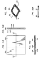
- Fig. 14 shows the magnet body BIM.
- Fig. 14A is a plan view thereof.
- Fig. 14B is a side view thereof.
- Fig. 14C is an elevational view thereof.
- the magnet body BIM is formed by piling up an inclined plate INN made of non-magnetic materials such as copper and having one predetermined inclined surface of the opposite surfaces, a plate HOM for homogenizing a magnetic field whose thickness is uniform and to be disposed at the inclined surface side of this inclined plate INN, a magnet plate MAG whose thickness is uniform and to be disposed at the upper surface side of this plate for homogenizing a magnetic field HOM and an inclined plate INM having an inclined surface and to be disposed at the upper surface side of this magnet body MAG and then integrating them by means of an epoxy system adhesive agent.
- an inclined plate INM having an inclined surface and to be disposed at the upper surface side of this magnet body MAG and then integrating them by means of an epoxy system adhesive agent.
- the bias coil is formed by thermal- depositing thermosetting resin coated on the outer surfaces of respective windings 40 and loading respective windings 40 and loading respective windings 40 by pressure-welding. Then, by cooling it, respective windings 40 are hardened in the united state of windings and thus having a predetermined picture frame.
- the present invention is designed to dispose the magnetic bubble memory chip loaded with the flexible substrate in the space section of the revolving magnetic circuit consisting of a picture frame core and to lay the overall body for confining a revolving magnetic field within the case, the body being made of good conducting materials, and to electrically connect the peripheral portion of the overall body with the case.
- a highly uniform revolving magnetic field can be obtained by a small VI product because of reducing the space for generating a leakage magnetic field and the magnetic bubble memory module which is designed to lower power con- supmtion, miniaturize and thin the overall form and ameliorate assembling efficiency can be obtained because of miniaturizing the case for confining a revolving magnetic field.
Landscapes
- Shielding Devices Or Components To Electric Or Magnetic Fields (AREA)
- Coils Or Transformers For Communication (AREA)
Applications Claiming Priority (6)
| Application Number | Priority Date | Filing Date | Title |
|---|---|---|---|
| JP15341/85 | 1985-01-31 | ||
| JP60015341A JPH0636310B2 (ja) | 1985-01-31 | 1985-01-31 | 磁気バブルメモリモジユ−ル |
| JP16540/85 | 1985-02-01 | ||
| JP60016540A JPH079750B2 (ja) | 1985-02-01 | 1985-02-01 | 配線基板 |
| JP60066456A JPH0646506B2 (ja) | 1985-04-01 | 1985-04-01 | 磁気バブルメモリ |
| JP66456/85 | 1985-04-01 |
Publications (3)
| Publication Number | Publication Date |
|---|---|
| EP0189926A2 true EP0189926A2 (de) | 1986-08-06 |
| EP0189926A3 EP0189926A3 (en) | 1989-03-15 |
| EP0189926B1 EP0189926B1 (de) | 1992-09-16 |
Family
ID=27280969
Family Applications (2)
| Application Number | Title | Priority Date | Filing Date |
|---|---|---|---|
| EP86101084A Expired - Lifetime EP0190642B1 (de) | 1985-01-31 | 1986-01-28 | Magnetischer Blasenspeichermodul |
| EP86101238A Expired EP0189926B1 (de) | 1985-01-31 | 1986-01-30 | Magnetischer Blasenspeichermodul |
Family Applications Before (1)
| Application Number | Title | Priority Date | Filing Date |
|---|---|---|---|
| EP86101084A Expired - Lifetime EP0190642B1 (de) | 1985-01-31 | 1986-01-28 | Magnetischer Blasenspeichermodul |
Country Status (3)
| Country | Link |
|---|---|
| US (1) | US4694423A (de) |
| EP (2) | EP0190642B1 (de) |
| DE (2) | DE3685125D1 (de) |
Cited By (1)
| Publication number | Priority date | Publication date | Assignee | Title |
|---|---|---|---|---|
| EP0200173A2 (de) | 1985-04-26 | 1986-11-05 | Hitachi, Ltd. | Magnetischer Blasenspeichermodul |
Families Citing this family (1)
| Publication number | Priority date | Publication date | Assignee | Title |
|---|---|---|---|---|
| CN112856902A (zh) * | 2019-11-12 | 2021-05-28 | 日立环球生活方案株式会社 | 冰箱 |
Family Cites Families (9)
| Publication number | Priority date | Publication date | Assignee | Title |
|---|---|---|---|---|
| US3836896A (en) * | 1972-06-29 | 1974-09-17 | Ibm | Non-volatile magnetic domain device having binary valued bias field excitation |
| CA1052912A (en) * | 1975-07-07 | 1979-04-17 | National Semiconductor Corporation | Gang bonding interconnect tape for semiconductive devices and method of making same |
| US4165535A (en) * | 1977-09-30 | 1979-08-21 | International Business Machines Corporation | Bubble memory drive system using a picture frame core and a reflection box |
| GB2011744A (en) * | 1977-12-29 | 1979-07-11 | Plessey Co Ltd | Improvements in or relating to magnetic domain devices |
| US4150440A (en) * | 1978-03-13 | 1979-04-17 | Control Data Corporation | Bubble memory package |
| US4209848A (en) * | 1978-06-16 | 1980-06-24 | International Business Machines Corporation | Magnetic domain device shield |
| US4247623A (en) * | 1979-06-18 | 1981-01-27 | Eastman Kodak Company | Blank beam leads for IC chip bonding |
| US4377854A (en) * | 1979-06-25 | 1983-03-22 | International Business Machines Corporation | Substrate for magnetic domain device |
| JPS6015888A (ja) * | 1983-07-06 | 1985-01-26 | Hitachi Ltd | 磁気バブルメモリモジユ−ル |
-
1986
- 1986-01-28 EP EP86101084A patent/EP0190642B1/de not_active Expired - Lifetime
- 1986-01-28 DE DE8686101084T patent/DE3685125D1/de not_active Expired - Lifetime
- 1986-01-29 US US06/823,647 patent/US4694423A/en not_active Expired - Lifetime
- 1986-01-30 EP EP86101238A patent/EP0189926B1/de not_active Expired
- 1986-01-30 DE DE8686101238T patent/DE3686728T2/de not_active Expired - Fee Related
Cited By (1)
| Publication number | Priority date | Publication date | Assignee | Title |
|---|---|---|---|---|
| EP0200173A2 (de) | 1985-04-26 | 1986-11-05 | Hitachi, Ltd. | Magnetischer Blasenspeichermodul |
Also Published As
| Publication number | Publication date |
|---|---|
| US4694423A (en) | 1987-09-15 |
| DE3686728D1 (de) | 1992-10-22 |
| EP0190642A3 (en) | 1989-03-15 |
| EP0189926A3 (en) | 1989-03-15 |
| DE3685125D1 (de) | 1992-06-11 |
| EP0189926B1 (de) | 1992-09-16 |
| EP0190642B1 (de) | 1992-05-06 |
| DE3686728T2 (de) | 1993-04-15 |
| EP0190642A2 (de) | 1986-08-13 |
Similar Documents
| Publication | Publication Date | Title |
|---|---|---|
| EP0189926B1 (de) | Magnetischer Blasenspeichermodul | |
| US4972369A (en) | Magnetic bubble memory module with interconnection member | |
| EP0200173B1 (de) | Magnetischer Blasenspeichermodul | |
| EP0201007A2 (de) | Messverfahren für das Haltefeld eines magnetischen Blasenspeichermoduls mit einem Bildrahmenkern | |
| EP0201009A2 (de) | Magnetischer Blasenspeichermodul | |
| JPH0697555B2 (ja) | 磁気バブルメモリ | |
| JPH0638314B2 (ja) | 磁気バブルメモリの特性評価方法 | |
| JPH0646508B2 (ja) | 磁気バブルメモリ | |
| JPH0697556B2 (ja) | 磁気バブルメモリ | |
| JPS61248283A (ja) | 磁気バブルメモリ装置 | |
| JPS61248282A (ja) | 磁気バブルメモリ装置の組立方法 | |
| JPS61227286A (ja) | 磁気バブルメモリ | |
| JPS61250888A (ja) | 磁気バブルメモリ | |
| JPH07114073B2 (ja) | 磁気バブルメモリ | |
| JPH0646512B2 (ja) | 磁気バブルメモリの特性評価方法 | |
| JPH0646511B2 (ja) | 磁気バブルメモリ | |
| JPH0646507B2 (ja) | 磁気バブルメモリ | |
| KR980011052A (ko) | 기입/판독 매트릭스 자기 헤드 및 그의 제조 방법 | |
| JPS61248290A (ja) | 磁気バブルメモリ装置 | |
| JPS622390B2 (de) | ||
| JPH0346185A (ja) | 磁気記憶素子 | |
| JPS61248292A (ja) | 磁気バブルメモリ装置 | |
| JPS61248291A (ja) | 磁気バブルメモリ装置 | |
| JPS61248289A (ja) | 磁気バブルメモリ装置 | |
| JPS61248285A (ja) | 磁気バブルメモリ装置 |
Legal Events
| Date | Code | Title | Description |
|---|---|---|---|
| PUAI | Public reference made under article 153(3) epc to a published international application that has entered the european phase |
Free format text: ORIGINAL CODE: 0009012 |
|
| 17P | Request for examination filed |
Effective date: 19860130 |
|
| AK | Designated contracting states |
Kind code of ref document: A2 Designated state(s): DE FR GB |
|
| PUAL | Search report despatched |
Free format text: ORIGINAL CODE: 0009013 |
|
| AK | Designated contracting states |
Kind code of ref document: A3 Designated state(s): DE FR GB |
|
| 17Q | First examination report despatched |
Effective date: 19900907 |
|
| GRAA | (expected) grant |
Free format text: ORIGINAL CODE: 0009210 |
|
| AK | Designated contracting states |
Kind code of ref document: B1 Designated state(s): DE FR GB |
|
| REF | Corresponds to: |
Ref document number: 3686728 Country of ref document: DE Date of ref document: 19921022 |
|
| ET | Fr: translation filed | ||
| PLBE | No opposition filed within time limit |
Free format text: ORIGINAL CODE: 0009261 |
|
| STAA | Information on the status of an ep patent application or granted ep patent |
Free format text: STATUS: NO OPPOSITION FILED WITHIN TIME LIMIT |
|
| 26N | No opposition filed | ||
| REG | Reference to a national code |
Ref country code: GB Ref legal event code: IF02 |
|
| PGFP | Annual fee paid to national office [announced via postgrant information from national office to epo] |
Ref country code: GB Payment date: 20021223 Year of fee payment: 18 |
|
| PGFP | Annual fee paid to national office [announced via postgrant information from national office to epo] |
Ref country code: FR Payment date: 20021230 Year of fee payment: 18 |
|
| PGFP | Annual fee paid to national office [announced via postgrant information from national office to epo] |
Ref country code: DE Payment date: 20030310 Year of fee payment: 18 |
|
| PG25 | Lapsed in a contracting state [announced via postgrant information from national office to epo] |
Ref country code: GB Free format text: LAPSE BECAUSE OF NON-PAYMENT OF DUE FEES Effective date: 20040130 |
|
| PG25 | Lapsed in a contracting state [announced via postgrant information from national office to epo] |
Ref country code: DE Free format text: LAPSE BECAUSE OF NON-PAYMENT OF DUE FEES Effective date: 20040803 |
|
| GBPC | Gb: european patent ceased through non-payment of renewal fee |
Effective date: 20040130 |
|
| PG25 | Lapsed in a contracting state [announced via postgrant information from national office to epo] |
Ref country code: FR Free format text: LAPSE BECAUSE OF NON-PAYMENT OF DUE FEES Effective date: 20040930 |
|
| REG | Reference to a national code |
Ref country code: FR Ref legal event code: ST |