EP0191476A2 - Zusammengesetzte Halbleiteranordnung und Verfahren zu ihrer Herstellung - Google Patents
Zusammengesetzte Halbleiteranordnung und Verfahren zu ihrer Herstellung Download PDFInfo
- Publication number
- EP0191476A2 EP0191476A2 EP86101774A EP86101774A EP0191476A2 EP 0191476 A2 EP0191476 A2 EP 0191476A2 EP 86101774 A EP86101774 A EP 86101774A EP 86101774 A EP86101774 A EP 86101774A EP 0191476 A2 EP0191476 A2 EP 0191476A2
- Authority
- EP
- European Patent Office
- Prior art keywords
- semiconductor substrate
- space
- annular groove
- mirror
- substrate
- Prior art date
- Legal status (The legal status is an assumption and is not a legal conclusion. Google has not performed a legal analysis and makes no representation as to the accuracy of the status listed.)
- Granted
Links
Images

Classifications
-
- H—ELECTRICITY
- H10—SEMICONDUCTOR DEVICES; ELECTRIC SOLID-STATE DEVICES NOT OTHERWISE PROVIDED FOR
- H10D—INORGANIC ELECTRIC SEMICONDUCTOR DEVICES
- H10D84/00—Integrated devices formed in or on semiconductor substrates that comprise only semiconducting layers, e.g. on Si wafers or on GaAs-on-Si wafers
- H10D84/01—Manufacture or treatment
- H10D84/0107—Integrating at least one component covered by H10D12/00 or H10D30/00 with at least one component covered by H10D8/00, H10D10/00 or H10D18/00, e.g. integrating IGFETs with BJTs
- H10D84/0109—Integrating at least one component covered by H10D12/00 or H10D30/00 with at least one component covered by H10D8/00, H10D10/00 or H10D18/00, e.g. integrating IGFETs with BJTs the at least one component covered by H10D12/00 or H10D30/00 being a MOS device
-
- H—ELECTRICITY
- H10—SEMICONDUCTOR DEVICES; ELECTRIC SOLID-STATE DEVICES NOT OTHERWISE PROVIDED FOR
- H10D—INORGANIC ELECTRIC SEMICONDUCTOR DEVICES
- H10D84/00—Integrated devices formed in or on semiconductor substrates that comprise only semiconducting layers, e.g. on Si wafers or on GaAs-on-Si wafers
- H10D84/01—Manufacture or treatment
- H10D84/0112—Integrating together multiple components covered by H10D8/00, H10D10/00 or H10D18/00, e.g. integrating multiple BJTs
-
- H—ELECTRICITY
- H10—SEMICONDUCTOR DEVICES; ELECTRIC SOLID-STATE DEVICES NOT OTHERWISE PROVIDED FOR
- H10D—INORGANIC ELECTRIC SEMICONDUCTOR DEVICES
- H10D84/00—Integrated devices formed in or on semiconductor substrates that comprise only semiconducting layers, e.g. on Si wafers or on GaAs-on-Si wafers
- H10D84/01—Manufacture or treatment
- H10D84/02—Manufacture or treatment characterised by using material-based technologies
- H10D84/03—Manufacture or treatment characterised by using material-based technologies using Group IV technology, e.g. silicon technology or silicon-carbide [SiC] technology
- H10D84/038—Manufacture or treatment characterised by using material-based technologies using Group IV technology, e.g. silicon technology or silicon-carbide [SiC] technology using silicon technology, e.g. SiGe
-
- H—ELECTRICITY
- H10—SEMICONDUCTOR DEVICES; ELECTRIC SOLID-STATE DEVICES NOT OTHERWISE PROVIDED FOR
- H10D—INORGANIC ELECTRIC SEMICONDUCTOR DEVICES
- H10D84/00—Integrated devices formed in or on semiconductor substrates that comprise only semiconducting layers, e.g. on Si wafers or on GaAs-on-Si wafers
- H10D84/40—Integrated devices formed in or on semiconductor substrates that comprise only semiconducting layers, e.g. on Si wafers or on GaAs-on-Si wafers characterised by the integration of at least one component covered by groups H10D12/00 or H10D30/00 with at least one component covered by groups H10D10/00 or H10D18/00, e.g. integration of IGFETs with BJTs
- H10D84/401—Combinations of FETs or IGBTs with BJTs
- H10D84/403—Combinations of FETs or IGBTs with BJTs and with one or more of diodes, resistors or capacitors
- H10D84/406—Combinations of FETs or IGBTs with vertical BJTs and with one or more of diodes, resistors or capacitors
-
- H—ELECTRICITY
- H10—SEMICONDUCTOR DEVICES; ELECTRIC SOLID-STATE DEVICES NOT OTHERWISE PROVIDED FOR
- H10D—INORGANIC ELECTRIC SEMICONDUCTOR DEVICES
- H10D84/00—Integrated devices formed in or on semiconductor substrates that comprise only semiconducting layers, e.g. on Si wafers or on GaAs-on-Si wafers
- H10D84/60—Integrated devices formed in or on semiconductor substrates that comprise only semiconducting layers, e.g. on Si wafers or on GaAs-on-Si wafers characterised by the integration of at least one component covered by groups H10D10/00 or H10D18/00, e.g. integration of BJTs
- H10D84/641—Combinations of only vertical BJTs
- H10D84/642—Combinations of non-inverted vertical BJTs of the same conductivity type having different characteristics, e.g. Darlington transistors
-
- H—ELECTRICITY
- H10—SEMICONDUCTOR DEVICES; ELECTRIC SOLID-STATE DEVICES NOT OTHERWISE PROVIDED FOR
- H10P—GENERIC PROCESSES OR APPARATUS FOR THE MANUFACTURE OR TREATMENT OF DEVICES COVERED BY CLASS H10
- H10P10/00—Bonding of wafers, substrates or parts of devices
- H10P10/12—Bonding of semiconductor wafers or semiconductor substrates to semiconductor wafers or semiconductor substrates
- H10P10/128—Bonding of semiconductor wafers or semiconductor substrates to semiconductor wafers or semiconductor substrates by direct semiconductor to semiconductor bonding
-
- H—ELECTRICITY
- H10—SEMICONDUCTOR DEVICES; ELECTRIC SOLID-STATE DEVICES NOT OTHERWISE PROVIDED FOR
- H10P—GENERIC PROCESSES OR APPARATUS FOR THE MANUFACTURE OR TREATMENT OF DEVICES COVERED BY CLASS H10
- H10P90/00—Preparation of wafers not covered by a single main group of this subclass, e.g. wafer reinforcement
- H10P90/19—Preparing inhomogeneous wafers
- H10P90/1904—Preparing vertically inhomogeneous wafers
- H10P90/1906—Preparing SOI wafers
-
- H—ELECTRICITY
- H10—SEMICONDUCTOR DEVICES; ELECTRIC SOLID-STATE DEVICES NOT OTHERWISE PROVIDED FOR
- H10W—GENERIC PACKAGES, INTERCONNECTIONS, CONNECTORS OR OTHER CONSTRUCTIONAL DETAILS OF DEVICES COVERED BY CLASS H10
- H10W10/00—Isolation regions in semiconductor bodies between components of integrated devices
- H10W10/01—Manufacture or treatment
- H10W10/011—Manufacture or treatment of isolation regions comprising dielectric materials
- H10W10/019—Manufacture or treatment of isolation regions comprising dielectric materials using epitaxial passivated integrated circuit [EPIC] processes
-
- H—ELECTRICITY
- H10—SEMICONDUCTOR DEVICES; ELECTRIC SOLID-STATE DEVICES NOT OTHERWISE PROVIDED FOR
- H10W—GENERIC PACKAGES, INTERCONNECTIONS, CONNECTORS OR OTHER CONSTRUCTIONAL DETAILS OF DEVICES COVERED BY CLASS H10
- H10W10/00—Isolation regions in semiconductor bodies between components of integrated devices
- H10W10/01—Manufacture or treatment
- H10W10/021—Manufacture or treatment of air gaps
-
- H—ELECTRICITY
- H10—SEMICONDUCTOR DEVICES; ELECTRIC SOLID-STATE DEVICES NOT OTHERWISE PROVIDED FOR
- H10W—GENERIC PACKAGES, INTERCONNECTIONS, CONNECTORS OR OTHER CONSTRUCTIONAL DETAILS OF DEVICES COVERED BY CLASS H10
- H10W10/00—Isolation regions in semiconductor bodies between components of integrated devices
- H10W10/01—Manufacture or treatment
- H10W10/061—Manufacture or treatment using SOI processes together with lateral isolation, e.g. combinations of SOI and shallow trench isolations
-
- H—ELECTRICITY
- H10—SEMICONDUCTOR DEVICES; ELECTRIC SOLID-STATE DEVICES NOT OTHERWISE PROVIDED FOR
- H10W—GENERIC PACKAGES, INTERCONNECTIONS, CONNECTORS OR OTHER CONSTRUCTIONAL DETAILS OF DEVICES COVERED BY CLASS H10
- H10W10/00—Isolation regions in semiconductor bodies between components of integrated devices
- H10W10/10—Isolation regions comprising dielectric materials
- H10W10/181—Semiconductor-on-insulator [SOI] isolation regions, e.g. buried oxide regions of SOI wafers
-
- H—ELECTRICITY
- H10—SEMICONDUCTOR DEVICES; ELECTRIC SOLID-STATE DEVICES NOT OTHERWISE PROVIDED FOR
- H10W—GENERIC PACKAGES, INTERCONNECTIONS, CONNECTORS OR OTHER CONSTRUCTIONAL DETAILS OF DEVICES COVERED BY CLASS H10
- H10W10/00—Isolation regions in semiconductor bodies between components of integrated devices
- H10W10/20—Air gaps
-
- H—ELECTRICITY
- H10—SEMICONDUCTOR DEVICES; ELECTRIC SOLID-STATE DEVICES NOT OTHERWISE PROVIDED FOR
- H10W—GENERIC PACKAGES, INTERCONNECTIONS, CONNECTORS OR OTHER CONSTRUCTIONAL DETAILS OF DEVICES COVERED BY CLASS H10
- H10W10/00—Isolation regions in semiconductor bodies between components of integrated devices
- H10W10/01—Manufacture or treatment
- H10W10/041—Manufacture or treatment of isolation regions comprising polycrystalline semiconductor materials
-
- H—ELECTRICITY
- H10—SEMICONDUCTOR DEVICES; ELECTRIC SOLID-STATE DEVICES NOT OTHERWISE PROVIDED FOR
- H10W—GENERIC PACKAGES, INTERCONNECTIONS, CONNECTORS OR OTHER CONSTRUCTIONAL DETAILS OF DEVICES COVERED BY CLASS H10
- H10W10/00—Isolation regions in semiconductor bodies between components of integrated devices
- H10W10/40—Isolation regions comprising polycrystalline semiconductor materials
Definitions
- the present invention relates to a composite semiconductor device and a process for manufacturing the same and, more particularly, to a composite semiconductor device which consists of a high voltage power element and an integrated circuit formed on one chip and which has a deep element isolation region, and a process for manufacturing the same.
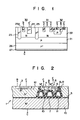
- a conventional composite semiconductor device consisting of a high voltage power element and an integrated circuit formed on one chip will be described with reference to Fig. 1.
- Fig. 1 is a sectional view showing a semiconductor device in which a power transistor section formed from the upper to lower surface of the semiconductor device and an IC section for controlling the transistor section are formed on one chip.
- n-type epitaxial layer 22 is formed on a p-type semiconductor substrate 21.
- Epitaxial layer 22 is divided into a power transistor section and a control IC section.
- Power transistor 30 in the power transistor section comprises n-type base region 25, forming part of epitaxial layer 22, p+- type emitter region 24 and n +- type base contact region 25a formed in base region 25, and p-type collector layer 21 and p +- type collector contact layer 26 constituting the semiconductor substrate.
- Collector electrode 27 is formed on the bottom surface of the structure.
- the control IC section comprises active elements (e.g., bipolar or MOS transistors) and passive elements (e.g., resistors, capacitors, and the like) formed in the epitaxial layer.
- active elements e.g., bipolar or MOS transistors
- passive elements e.g., resistors, capacitors, and the like
- the number of elements differs depending on the type of device, but in general, several to several tens of elements are formed.
- p-channel MOS transistor 31 and bipolar transistor 32 are exemplified as active elements.
- p++- type region 23 isolates the power transistor section from'the control IC section and reaches as far as p-type collector layer 21.
- Epitaxial layer 22, in which the control IC section is formed, is thus surrounded by region 23 and collector layer 21. More specifically, a pn junction is formed around the control IC section. Normally, since collector electrode 27 is fixed at a minimum potential in the substrate, the pn junction is reverse-biased during turn-on of the device, thus forming a depletion layer which performs element isolation.
- a composite semiconductor device comprising:
- the annular groove can be filled with the first insulating layer but need not be completely filled, and the first insulating layer can be formed only on its side walls.
- the groove is completely filled with a filling material by a CVD process.
- an insulating material such as Si0 2 , Si 3 N 4 , or the like can be used as the filling material, polycrystalline silicon having substantially the same thermal expansion coefficient as the silicon substrate is preferable.
- a bonding layer is normally formed at a bonding interface between the first and second semiconductor substrates.
- the surface roughness of the mirror-polished surface is preferably 500 A or less.
- surface roughness is given by a maximum height (Rmax) defined by JIS B-0601 (1982).
- An optical polishing method can be adopted as a mirror polishing method.
- the mirror-polished surface is preferably washed with water, surfactant, organic solvent, acid solution, or the like to remove stain films or contaminants (e.g., fine particles, absorbed ions, organic material, or inorganic material).
- stain films or contaminants e.g., fine particles, absorbed ions, organic material, or inorganic material.
- the mirror-polished surfaces of the first and second semiconductor substrates must be bonded in a clean atmosphere.
- the heating temperature for bonding preferably falls within the range of 1,000 to 1,200°C. High temperatures, at which the first and second semiconductor substrates may fuse together, should be avoided.
- the first functional element is reliably isolated from the second functional element by the deep insulating layer, thus achieving element isolation with a high breakdown voltage.
- the first functional element will not be influenced by heat from the second functional element due to the presence of the space therebetween.
- vertical type power transistor 2 as a second functional element, and an IC, as a first functional element, for controlling transistor 2 are formed in composite silicon substrate 1.
- IC as a first functional element, for controlling transistor 2
- planar transistor 6 is shown as a component of the control IC.
- Composite silicon substrate 1 is formed by bonding together n -type first silicon substrate la and n +- type second silicon substrate lb.
- IC forming portion 4 in which the control IC is formed, is a rectangular platelike surface layer in first silicon substrate la havig a thickness of about 20 ⁇ m.
- Two pillars 5 are formed on the bottom surface of portion 4. The side surfaces of portion 4 are covered with silicon oxide layer 7 and filling material layer 8. Portion 4 is thus isolated from the remaining portion of substrate la by layers 7 and 8.
- Space 11 is formed below portion 4 in substrate la, and two pillars 5 project downward in space 11 from the bottom surface of portion 4.
- Surfaces of substrates la and lb (including the surfaces of pillars 5) exposed to space 11 are covered with silicon oxide layer 7 and filling material layer 8.
- Silicon oxide layer 10 is sandwiched between pillars 5 and substrate lb to isolate them from each other. In this way, portion 4 and pillars 5 projecting therefrom are electrically isolated from the remaining portion of substrate la and from substrate lb.
- npn transistor 2 is formed in the remaining portion of substrate la.
- the collector contact layer of transistor 2 is formed on a surface opposite the bonding surface of substrate lb.
- the composite semiconductor device is prepared as follows.
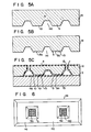
- Figs. 3A to 3F are sectional views showing major steps in the manufacture of the device of the present invention
- Fig. 4 is a plan view of substrate la after the step in Fig. 3A.
- N -type first silicon substrate la and n +- type second silicon substrate lb are prepared.
- One surface of each is mirror-polished to obtain a surface roughness of 500 A or less, thus forming first and second mirror-polished surfaces.
- Substrates la and lb can be degreased if needed. Rectangular recess lla having a mesa cross-section and a depth of about 80 ⁇ m is then formed in the first mirror-polished surface of substrate la.
- Substrate la is patterned to leave two pillars 5 in recess lla, as shown in Fig. 3A.
- Mesa recess lla is formed by chemical etching using an oxide film (not shown) as a mask, but can be formed by reactive ion etching (to be referred to as RIE hereinafter) (Figs. 3A and 4).
- the first and second mirror-polished surfaces of substrates la and lb are placed in contact with each other in a clean atmosphere so that no foreign substances are present therebetween, and are then heated to 1,200°C to be bonded together. This is performed by a vacuum heating apparatus.
- reference numeral 3 denotes a bonding layer formed at the boundary between substrates la and lb (Fig. 3B).
- the surface of substrate la is lapped to reduce its thickness to 100 ⁇ m, so that the thickness of the portion of substrate la above recess 11 is reduced to 20 pm (Fig. 3C).
- 3- u m thick oxide (Si0 2 ) film 13 is formed on the lapped surface of substrate la.
- a resist is patterned by a photoetching process method (PEP method), and annular groove 12a is formed in the portion of film 13 corresponding to the peripheral edge portion of recess 11 by RIE.
- Substrate la is then etched by RIE using film 13 as a mask to form annular groove 12, which extends to recess 11.
- recess 11 is open to the outer atmosphere through groove 12.
- Portion (the same as the IC forming portion above) 4 of substrate la (thickness: 20 ⁇ m) lying on recess 11 is separated from the remaining portion of substrate la by groove 12, but can be supported by two pillars 5 so as not to be broken (Fig. 3D).
- Thermal oxidation is then performed via groove 12 in a wet oxygen atmosphere.
- insulating oxide layer 10 is formed between pillars 5 and substrate lb and until pillars 5 are electrically isolated from bonding layer 3 and substrate lb adjacent thereto.
- oxide layer 7 is formed on the side walls of groove 12 and the surfaces of pillars 5.
- Thermal oxidation time is determined by an external oxide layer thickness monitor or test samples.
- insulating layer 10 is formed on the bottom portions of pillars 5. In general, however, the insulating layer is formed on the portion of a pillar which is thinnest and oxidizes most easily (Fig. 3E).
- Groove 12, whose side walls were oxidized, is filled with polycrystalline silicon by a reduced- pressure CVD method, thus air-tightly sealing recess 11.
- Polycrystalline silicon is also deposited on the inner surface of recess 11.
- this deposited portion is not related to the present invention.
- filling material layer 8 formed by filling groove 12 with a filling material, seals recess 11, flattens the exposed surface of substrate la, and prevents attachment of foreign substances to recess 11 which cannot be removed later. Since recess 11 is sealed under reduced pressure, internal air will not expand in subsequent heating process, thus preventing damage to the substrate.
- the polycrystalline silicon film, oxide film, and the like attached to the surface of the substrate are removed, and a control IC and power transistor 2 are formed in IC forming portion 4 and in the remaining portion, respectively, of substrate la.
- Substrate lb acts as the collector contact layer of power transistor 2. In this case, the effect of the barrier caused by bonding layer 3 between substrates la and lb on the function of power transistor 2 is negligible.
- Fig. 5A is a sectional view showing substrate la after deep mesa etching. More specifically, 80- p m rectangular recess lla having a mesa cross-section is formed in a first mirror-polished surface of substrate la by deep chemical etching. In this case, two pillars 5 are left in the recess region. However, it is difficult to leave bonding surface 13, which will subsequently be bonded to substrate lb, with high precision by this etching method.
- Fig. 5B is a sectional view of substrate 1 after shallow mesa etching
- Fig. 6 is a plan view thereof.
- a plurality (e.g., 16) of ' short pillars 5a are formed on surface 13.
- bonding surface 13a of each pillar 5a has an area of 2 um 2 .
- Shallow mesa recess llb is connected with deep recess lla.
- Fig. 5C corresponds with Fig. 3E in Example 1 and is a sectional view showing the state after annular groove 12 was formed and thermal oxidation was performed.
- insulating oxide layer 10 is formed in the same manner as in Example 1, and pillars 5a are electrically isolated from substrate lb.
- oxide layer 7 is formed on the side walls of groove 12 and the surfaces of pillars 5 and 5a.
- IC forming portion 4 is dielectrically separated from the remaining portion of substrate la and from substrate lb. The other steps are the same as those in Example 1.
- n +- type impurity be ion-implanted in substrate la so as to form an n +- type region on the inner surfaces of recesses lla after pillars 5 are formed by selective etching. In this way, the series resistance of the collector can be reduced.
- an isolation breakdown voltage of 1,000 V or higher impossible to obtain with the conventional pn junction separation method, can be realized. Since a large area of an IC forming portion for a control IC is adjacent to a space, heat from a power element (e.g., a power transistor) can be dispersed, and changes in IC characteristics due to heat can be reduced. In addition, isolation capacity and parasitic element effect are reduced when compared with conventional devices, thus providing a stable composite semiconductor device with high reliability.
- a power element e.g., a power transistor
Landscapes
- Element Separation (AREA)
- Bipolar Integrated Circuits (AREA)
Applications Claiming Priority (2)
| Application Number | Priority Date | Filing Date | Title |
|---|---|---|---|
| JP24389/85 | 1985-02-13 | ||
| JP60024389A JPS61184843A (ja) | 1985-02-13 | 1985-02-13 | 複合半導体装置とその製造方法 |
Publications (3)
| Publication Number | Publication Date |
|---|---|
| EP0191476A2 true EP0191476A2 (de) | 1986-08-20 |
| EP0191476A3 EP0191476A3 (en) | 1986-10-22 |
| EP0191476B1 EP0191476B1 (de) | 1989-11-08 |
Family
ID=12136809
Family Applications (1)
| Application Number | Title | Priority Date | Filing Date |
|---|---|---|---|
| EP86101774A Expired EP0191476B1 (de) | 1985-02-13 | 1986-02-12 | Zusammengesetzte Halbleiteranordnung und Verfahren zu ihrer Herstellung |
Country Status (4)
| Country | Link |
|---|---|
| US (1) | US4710794A (de) |
| EP (1) | EP0191476B1 (de) |
| JP (1) | JPS61184843A (de) |
| DE (1) | DE3666901D1 (de) |
Cited By (7)
| Publication number | Priority date | Publication date | Assignee | Title |
|---|---|---|---|---|
| DE4016695A1 (de) * | 1989-05-24 | 1990-11-29 | Nissan Motor | Halbleiterbauelement |
| US5212109A (en) * | 1989-05-24 | 1993-05-18 | Nissan Motor Co., Ltd. | Method for forming PN junction isolation regions by forming buried regions of doped polycrystalline or amorphous semiconductor |
| WO1993017459A3 (de) * | 1992-02-12 | 1993-10-28 | Daimler Benz Ag | Verfahren zur herstellung einer halbleiterstruktur und nach dem verfahren hergestellte halbleiterstruktur |
| EP0596264A1 (de) * | 1992-10-07 | 1994-05-11 | Daimler-Benz Aktiengesellschaft | Halbleiterbauelement mit hoher Durchbruchsspannung |
| WO1999067820A1 (de) * | 1998-06-22 | 1999-12-29 | Fraunhofer-Gesellschaft zur Förderung der angewandten Forschung e.V. | Verfahren zur fertigung von dünnen substratschichten |
| EP1043769A1 (de) * | 1999-04-07 | 2000-10-11 | STMicroelectronics S.r.l. | Herstellungsverfahren für eine Halbleiterscheibe mit durch isolierendes Material getrennten monokristallinen Gebieten, insbesondere zur Herstellung integrierter Leistungsbauelemente, und dadurch hergestellte Scheibe |
| WO2004038790A1 (ja) * | 2002-10-22 | 2004-05-06 | Sumitomo Mitsubishi Silicon Corporation | 貼り合わせsoi基板およびその製造方法ならびに半導体装置 |
Families Citing this family (44)
| Publication number | Priority date | Publication date | Assignee | Title |
|---|---|---|---|---|
| US4949162A (en) * | 1987-06-05 | 1990-08-14 | Hitachi, Ltd. | Semiconductor integrated circuit with dummy pedestals |
| JP2586422B2 (ja) * | 1987-10-20 | 1997-02-26 | 日本電装株式会社 | 誘電体分離型複合集積回路装置の製造方法 |
| JPH01179342A (ja) * | 1988-01-05 | 1989-07-17 | Toshiba Corp | 複合半導体結晶体 |
| JP2788269B2 (ja) * | 1988-02-08 | 1998-08-20 | 株式会社東芝 | 半導体装置およびその製造方法 |
| JP2685244B2 (ja) * | 1988-09-30 | 1997-12-03 | 株式会社日本自動車部品総合研究所 | 半導体装置の製造方法 |
| JPH0656865B2 (ja) * | 1988-10-13 | 1994-07-27 | 株式会社東芝 | 高耐圧素子用接着基板 |
| US5416354A (en) * | 1989-01-06 | 1995-05-16 | Unitrode Corporation | Inverted epitaxial process semiconductor devices |
| US5164218A (en) * | 1989-05-12 | 1992-11-17 | Nippon Soken, Inc. | Semiconductor device and a method for producing the same |
| US5264720A (en) * | 1989-09-22 | 1993-11-23 | Nippondenso Co., Ltd. | High withstanding voltage transistor |
| JPH0821619B2 (ja) * | 1989-10-13 | 1996-03-04 | 株式会社東芝 | 半導体装置 |
| DD290077A5 (de) * | 1989-12-15 | 1991-05-16 | ���@����������@��k�� | Verfahren zum bonden von halbleitersubstraten |
| JPH03283636A (ja) * | 1990-03-30 | 1991-12-13 | Nippon Soken Inc | 半導体基板の製造方法 |
| DE69232432T2 (de) * | 1991-11-20 | 2002-07-18 | Canon K.K., Tokio/Tokyo | Verfahren zur Herstellung einer Halbleiteranordnung |
| US5389569A (en) * | 1992-03-03 | 1995-02-14 | Motorola, Inc. | Vertical and lateral isolation for a semiconductor device |
| US5413962A (en) * | 1994-07-15 | 1995-05-09 | United Microelectronics Corporation | Multi-level conductor process in VLSI fabrication utilizing an air bridge |
| US5796883A (en) * | 1995-09-04 | 1998-08-18 | Nec Corporation | Optical integrated circuit and method for fabricating the same |
| US5949144A (en) * | 1996-05-20 | 1999-09-07 | Harris Corporation | Pre-bond cavity air bridge |
| DE69931890T2 (de) * | 1999-04-06 | 2007-01-11 | Stmicroelectronics S.R.L., Agrate Brianza | Integrierter Leistungsschaltkreis mit vertikalem Stromfluss und dessen Herstellungsverfahren |
| JP3957038B2 (ja) * | 2000-11-28 | 2007-08-08 | シャープ株式会社 | 半導体基板及びその作製方法 |
| FR2819630B1 (fr) | 2001-01-12 | 2003-08-15 | St Microelectronics Sa | Dispositif semi-conducteur a zone isolee et procede de fabrication correspondant |
| WO2003010806A2 (en) * | 2001-07-26 | 2003-02-06 | Massachusetts Institute Of Technology | Semiconductor substrate bonding by mass transport growth fusion |
| DE10144343A1 (de) * | 2001-09-10 | 2003-03-27 | Perkinelmer Optoelectronics | Sensor zum berührugslosen Messen einer Temperatur |
| JP4020195B2 (ja) | 2002-12-19 | 2007-12-12 | 三菱電機株式会社 | 誘電体分離型半導体装置の製造方法 |
| US20070057289A1 (en) | 2004-01-10 | 2007-03-15 | Davies Robert B | Power semiconductor device and method therefor |
| FR2875947B1 (fr) * | 2004-09-30 | 2007-09-07 | Tracit Technologies | Nouvelle structure pour microelectronique et microsysteme et procede de realisation |
| FR2876220B1 (fr) * | 2004-10-06 | 2007-09-28 | Commissariat Energie Atomique | Procede d'elaboration de structures empilees mixtes, a zones isolantes diverses et/ou zones de conduction electrique verticale localisees. |
| US8530963B2 (en) * | 2005-01-06 | 2013-09-10 | Estivation Properties Llc | Power semiconductor device and method therefor |
| JP5662001B2 (ja) * | 2005-12-21 | 2015-01-28 | クロメック リミテッド | 半導体デバイス及びその製造方法 |
| GB2433648A (en) * | 2005-12-21 | 2007-06-27 | Durham Scient Crystals Ltd | Radiation detector formed by deposition of bulk semiconductor crystal layers |
| FR2897982B1 (fr) | 2006-02-27 | 2008-07-11 | Tracit Technologies Sa | Procede de fabrication des structures de type partiellement soi, comportant des zones reliant une couche superficielle et un substrat |
| JP2006310838A (ja) * | 2006-04-05 | 2006-11-09 | Hvvi Semiconductors Inc | パワー半導体装置およびそのための方法 |
| JP2006310836A (ja) * | 2006-04-05 | 2006-11-09 | Hvvi Semiconductors Inc | パワー半導体装置およびそのための方法 |
| DE102007001523A1 (de) * | 2007-01-10 | 2008-07-17 | Infineon Technologies Ag | Halbleiterschaltungsanordnung und Verfahren zu deren Herstellung |
| US9666703B2 (en) * | 2014-12-17 | 2017-05-30 | Great Wall Semiconductor Corporation | Semiconductor devices with cavities |
| US10461152B2 (en) | 2017-07-10 | 2019-10-29 | Globalfoundries Inc. | Radio frequency switches with air gap structures |
| WO2019083729A1 (en) * | 2017-10-23 | 2019-05-02 | Trustees Of Boston University | ENHANCED THERMAL TRANSPORT THROUGH INTERFACES |
| US10446643B2 (en) | 2018-01-22 | 2019-10-15 | Globalfoundries Inc. | Sealed cavity structures with a planar surface |
| US11056382B2 (en) * | 2018-03-19 | 2021-07-06 | Globalfoundries U.S. Inc. | Cavity formation within and under semiconductor devices |
| US11410872B2 (en) * | 2018-11-30 | 2022-08-09 | Globalfoundries U.S. Inc. | Oxidized cavity structures within and under semiconductor devices |
| US10923577B2 (en) | 2019-01-07 | 2021-02-16 | Globalfoundries U.S. Inc. | Cavity structures under shallow trench isolation regions |
| US11127816B2 (en) | 2020-02-14 | 2021-09-21 | Globalfoundries U.S. Inc. | Heterojunction bipolar transistors with one or more sealed airgap |
| US11764258B2 (en) * | 2020-12-01 | 2023-09-19 | Globalfoundries U.S. Inc. | Airgap isolation structures |
| US11881506B2 (en) | 2021-07-27 | 2024-01-23 | Globalfoundries U.S. Inc. | Gate structures with air gap isolation features |
| US20240250157A1 (en) * | 2023-01-20 | 2024-07-25 | Globalfoundries U.S. Inc. | Heater terminal contacts |
Family Cites Families (10)
| Publication number | Priority date | Publication date | Assignee | Title |
|---|---|---|---|---|
| US3412296A (en) * | 1965-10-19 | 1968-11-19 | Sprague Electric Co | Monolithic structure with threeregion or field effect complementary transistors |
| JPS5423388A (en) * | 1977-07-22 | 1979-02-21 | Hitachi Ltd | Semiconductor integrated-circuit device and its manufacture |
| JPS5440084A (en) * | 1977-09-05 | 1979-03-28 | Fujitsu Ltd | Semiconductor device and manufacture thereof |
| DE2926741C2 (de) * | 1979-07-03 | 1982-09-09 | Licentia Patent-Verwaltungs-Gmbh, 6000 Frankfurt | Feldeffekt-Transistor und Verfahren zu seiner Herstellung |
| US4411060A (en) * | 1981-07-06 | 1983-10-25 | Western Electric Co., Inc. | Method of manufacturing dielectrically-isolated single-crystal semiconductor substrates |
| US4502913A (en) * | 1982-06-30 | 1985-03-05 | International Business Machines Corporation | Total dielectric isolation for integrated circuits |
| US4661832A (en) * | 1982-06-30 | 1987-04-28 | International Business Machines Corporation | Total dielectric isolation for integrated circuits |
| US4467521A (en) * | 1983-08-15 | 1984-08-28 | Sperry Corporation | Selective epitaxial growth of gallium arsenide with selective orientation |
| JPS60113455A (ja) * | 1983-11-24 | 1985-06-19 | Hitachi Ltd | 半導体集積回路装置 |
| EP0161740B1 (de) * | 1984-05-09 | 1991-06-12 | Kabushiki Kaisha Toshiba | Verfahren zur Herstellung eines Halbleitersubstrates |
-
1985
- 1985-02-13 JP JP60024389A patent/JPS61184843A/ja active Granted
-
1986
- 1986-02-12 EP EP86101774A patent/EP0191476B1/de not_active Expired
- 1986-02-12 US US06/828,536 patent/US4710794A/en not_active Expired - Lifetime
- 1986-02-12 DE DE8686101774T patent/DE3666901D1/de not_active Expired
Cited By (9)
| Publication number | Priority date | Publication date | Assignee | Title |
|---|---|---|---|---|
| DE4016695A1 (de) * | 1989-05-24 | 1990-11-29 | Nissan Motor | Halbleiterbauelement |
| US5212109A (en) * | 1989-05-24 | 1993-05-18 | Nissan Motor Co., Ltd. | Method for forming PN junction isolation regions by forming buried regions of doped polycrystalline or amorphous semiconductor |
| WO1993017459A3 (de) * | 1992-02-12 | 1993-10-28 | Daimler Benz Ag | Verfahren zur herstellung einer halbleiterstruktur und nach dem verfahren hergestellte halbleiterstruktur |
| US5591665A (en) * | 1992-02-12 | 1997-01-07 | Daimler-Benz Aktiengesellschaft | Process for producing a semiconductor structure including a plurality of vertical semiconductor devices and at least one lateral semiconductor device integrated in a semiconductor body |
| EP0596264A1 (de) * | 1992-10-07 | 1994-05-11 | Daimler-Benz Aktiengesellschaft | Halbleiterbauelement mit hoher Durchbruchsspannung |
| WO1999067820A1 (de) * | 1998-06-22 | 1999-12-29 | Fraunhofer-Gesellschaft zur Förderung der angewandten Forschung e.V. | Verfahren zur fertigung von dünnen substratschichten |
| EP1043769A1 (de) * | 1999-04-07 | 2000-10-11 | STMicroelectronics S.r.l. | Herstellungsverfahren für eine Halbleiterscheibe mit durch isolierendes Material getrennten monokristallinen Gebieten, insbesondere zur Herstellung integrierter Leistungsbauelemente, und dadurch hergestellte Scheibe |
| WO2004038790A1 (ja) * | 2002-10-22 | 2004-05-06 | Sumitomo Mitsubishi Silicon Corporation | 貼り合わせsoi基板およびその製造方法ならびに半導体装置 |
| US7253082B2 (en) | 2002-10-22 | 2007-08-07 | Sumitomo Mitsubishi Silicon Corporation | Pasted SOI substrate, process for producing the same and semiconductor device |
Also Published As
| Publication number | Publication date |
|---|---|
| US4710794A (en) | 1987-12-01 |
| JPH0473621B2 (de) | 1992-11-24 |
| JPS61184843A (ja) | 1986-08-18 |
| EP0191476B1 (de) | 1989-11-08 |
| DE3666901D1 (en) | 1989-12-14 |
| EP0191476A3 (en) | 1986-10-22 |
Similar Documents
| Publication | Publication Date | Title |
|---|---|---|
| EP0191476B1 (de) | Zusammengesetzte Halbleiteranordnung und Verfahren zu ihrer Herstellung | |
| JP2788269B2 (ja) | 半導体装置およびその製造方法 | |
| US5403769A (en) | Process for producing a semiconductor device | |
| EP0182032B1 (de) | SoI-Halbleiteranordnung und Verfahren zu ihrer Herstellung | |
| US5004705A (en) | Inverted epitaxial process | |
| US6084284A (en) | Integrated circuit including inverted dielectric isolation | |
| EP0176747B1 (de) | Halbleitersubstrat aus Silicium mit vergrabener Isolierschicht und Verfahren zur Herstellung | |
| US3954523A (en) | Process for fabricating devices having dielectric isolation utilizing anodic treatment and selective oxidation | |
| US6277703B1 (en) | Method for manufacturing an SOI wafer | |
| EP0615286B1 (de) | Halbleiteranordnung mit einer Isolationszone | |
| EP0323856B1 (de) | Substratsstruktur für zusammengesetztes Halbleiterbauelement | |
| EP0653785B1 (de) | Dielektrisch isolierte Halbleiteranordnung | |
| EP0164646A2 (de) | Vergrabene Feldabschirmung für integrierte Schaltung | |
| US5164813A (en) | New diode structure | |
| JP3014012B2 (ja) | 半導体装置の製造方法 | |
| EP0193116B1 (de) | Verfahren zum Herstellen eines Halbleiterbauelements mit einem Graben | |
| US5476809A (en) | Semiconductor device and method of manufacturing the same | |
| EP0112489A1 (de) | Halbleiterbauelement mit kompakter Isolation und Verfahren zu seiner Herstellung | |
| US6104078A (en) | Design for a semiconductor device having elements isolated by insulating regions | |
| US5406113A (en) | Bipolar transistor having a buried collector layer | |
| US5763931A (en) | Semiconductor device with SOI structure and fabrication method thereof | |
| JP2979554B2 (ja) | 半導体装置の製造方法 | |
| EP0789403B1 (de) | Zener-Zap-Diode und Verfahren zur Herstellung | |
| JP3148766B2 (ja) | 半導体装置 | |
| JPH0629376A (ja) | 集積回路装置 |
Legal Events
| Date | Code | Title | Description |
|---|---|---|---|
| PUAI | Public reference made under article 153(3) epc to a published international application that has entered the european phase |
Free format text: ORIGINAL CODE: 0009012 |
|
| 17P | Request for examination filed |
Effective date: 19860212 |
|
| AK | Designated contracting states |
Kind code of ref document: A2 Designated state(s): DE FR GB NL |
|
| PUAL | Search report despatched |
Free format text: ORIGINAL CODE: 0009013 |
|
| AK | Designated contracting states |
Kind code of ref document: A3 Designated state(s): DE FR GB NL |
|
| 17Q | First examination report despatched |
Effective date: 19890222 |
|
| GRAA | (expected) grant |
Free format text: ORIGINAL CODE: 0009210 |
|
| AK | Designated contracting states |
Kind code of ref document: B1 Designated state(s): DE FR GB NL |
|
| REF | Corresponds to: |
Ref document number: 3666901 Country of ref document: DE Date of ref document: 19891214 |
|
| ET | Fr: translation filed | ||
| PLBE | No opposition filed within time limit |
Free format text: ORIGINAL CODE: 0009261 |
|
| STAA | Information on the status of an ep patent application or granted ep patent |
Free format text: STATUS: NO OPPOSITION FILED WITHIN TIME LIMIT |
|
| 26N | No opposition filed | ||
| PGFP | Annual fee paid to national office [announced via postgrant information from national office to epo] |
Ref country code: GB Payment date: 19970203 Year of fee payment: 12 |
|
| PGFP | Annual fee paid to national office [announced via postgrant information from national office to epo] |
Ref country code: FR Payment date: 19970211 Year of fee payment: 12 |
|
| PGFP | Annual fee paid to national office [announced via postgrant information from national office to epo] |
Ref country code: DE Payment date: 19970221 Year of fee payment: 12 |
|
| PG25 | Lapsed in a contracting state [announced via postgrant information from national office to epo] |
Ref country code: GB Free format text: LAPSE BECAUSE OF NON-PAYMENT OF DUE FEES Effective date: 19980212 |
|
| PG25 | Lapsed in a contracting state [announced via postgrant information from national office to epo] |
Ref country code: FR Free format text: THE PATENT HAS BEEN ANNULLED BY A DECISION OF A NATIONAL AUTHORITY Effective date: 19980228 |
|
| GBPC | Gb: european patent ceased through non-payment of renewal fee |
Effective date: 19980212 |
|
| PG25 | Lapsed in a contracting state [announced via postgrant information from national office to epo] |
Ref country code: DE Free format text: LAPSE BECAUSE OF NON-PAYMENT OF DUE FEES Effective date: 19981103 |
|
| REG | Reference to a national code |
Ref country code: FR Ref legal event code: ST |
|
| PGFP | Annual fee paid to national office [announced via postgrant information from national office to epo] |
Ref country code: NL Payment date: 20050203 Year of fee payment: 20 |
|
| PG25 | Lapsed in a contracting state [announced via postgrant information from national office to epo] |
Ref country code: NL Free format text: LAPSE BECAUSE OF EXPIRATION OF PROTECTION Effective date: 20060212 |
|
| NLV7 | Nl: ceased due to reaching the maximum lifetime of a patent |
Effective date: 20060212 |