EP0194468A2 - Commutateur de sélection électronique pour la sélection et une éventuelle atténuation des fréquences radio et télévision - Google Patents
Commutateur de sélection électronique pour la sélection et une éventuelle atténuation des fréquences radio et télévision Download PDFInfo
- Publication number
- EP0194468A2 EP0194468A2 EP86101959A EP86101959A EP0194468A2 EP 0194468 A2 EP0194468 A2 EP 0194468A2 EP 86101959 A EP86101959 A EP 86101959A EP 86101959 A EP86101959 A EP 86101959A EP 0194468 A2 EP0194468 A2 EP 0194468A2
- Authority
- EP
- European Patent Office
- Prior art keywords
- chain
- inputs
- output
- input
- electronic selector
- Prior art date
- Legal status (The legal status is an assumption and is not a legal conclusion. Google has not performed a legal analysis and makes no representation as to the accuracy of the status listed.)
- Withdrawn
Links
Images


Classifications
-
- H—ELECTRICITY
- H03—ELECTRONIC CIRCUITRY
- H03K—PULSE TECHNIQUE
- H03K17/00—Electronic switching or gating, i.e. not by contact-making and –breaking
- H03K17/51—Electronic switching or gating, i.e. not by contact-making and –breaking characterised by the components used
- H03K17/74—Electronic switching or gating, i.e. not by contact-making and –breaking characterised by the components used by the use, as active elements, of diodes
- H03K17/76—Switching arrangements with several input- or output-terminals, e.g. multiplexers, distributors
Definitions
- This invention involves an electronic selector switch for selection and the eventual damping of radio and television frequencies. More particularly; the invention also involves an electronic selector switch for the selection and eventual damping of radio and television frequencies preferably operating on the 40 + 200 MHz band and utilizable for the reception of radio and television signals either by ether or cable.
- the selector switch object of this invention, contains semiconductor circuits through which groups of RF signals possibly adjacent one to the other, and/or with different signal levels coming from one or more sources of emission, generic or from transmitting stations with different or equal orientation and applied respectively to two or more of the selector switch's inputs, they are conveyed around its output with possible modification of intensity and sent to a received which is rendered interference free so that the reception of the broadcast is pleasant and perfect.
- the object of the present invention is to produce an electronic selector switch which does not have the above mentioned disadvantages.
- This invention solves the problem by means of an electronic selector switch for Radio and television frequencies through which the following results are obtained:
- the advantages achieved with the present invention essentially consist in the fact that signals coming from any transmitting source, groupable in two or more groups of channels which are which are technically compatible, amplified or not and sent respectively to two or more selector inputs, can be selected in such a way that the signals get to the receivers interference free, even if they are conveyed around one single drop wire for television antenna or sent directly to the only input of the receiver tuner.
- a good receiver which is particularly selective can receive a lot more radio and television programmes even in critical areas where, contrary to what actually occured up to now, due to the present commutation systems applied to receiving antennae or other which degradate the signals before they reach the receivers' TUNER.
- Today's selectors can be constructed in various ways and adapted to various, even well known, commutation systems; in particular, they can be constructed with their components erected in the air or on printed circuits; they can also be constructed apart from or incorporated into radio receivers or in portable or non- portable antenna systems and in generic RF commutation systems.
- Commutation control can be carried out both with separate systems or through receiver voltage, and the operation of the selector can either be manual or by remote control.
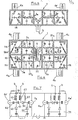
- electronic selector n°1 for radio and television frequencies consists of one or more PIN diodes 3, placed in series and forming the 23 chains, which connect the RF inputs 4, to the output 5, of selector 1.
- Each 23 chain is connected at one extremity to an RF input and at the other to a sole 5A point; this point is connected either directly or through polarization circuits, filter and/or insulator, with output 5.
- Each input 4 is connected to a source of RF signals of the following kinds: single receiving antennae, groups of signals which are already formed, coming from different stations, signals coming from television cameras or other.
- the output 5 is connected to the input of a user set, such as a radio/television set or a video recorder or a video tape player or similar, through a feed-cable or similar.
- a user set such as a radio/television set or a video recorder or a video tape player or similar
- Figure 1 illustrates the way in which it Is possible to obtain commutation at radio frequency for a PIN diode selector with two or more inputs; with this system it is possible to create selectors with any number of inputs, since the activation of one of these automatically excludes the feedthrough at radio frequency of the others.
- the application of positive voltage, with respect to the mass, on input 10, and none on 11, 12 and 13, through the capacitator feedthrough 22, and the RF 8A block coil this reaches the 3A PIN diodes.
- These 3A PIN diodes expose the anode to positive voltage and the mass cathode through resistance 7 and they enter into conduction since a current determined by the voltage applied in 10 and from the resistivity value of resistance 7, runs through them.
- the radio frequency signals present on input 4A get to the 8A block coil through the 2A isolating capacitator. This 8A coil prevents the transit of signals towards input 10.
- the RF signals go to resistance 7, which, being of high value (for example: 470 + 1000 Ohm) with respect to the selector impedance (for example: 50 + 90 Ohm) there is a mass discharge on only a small part of these signals, they therefore reach output 5 through the insulation condenser 6 with a minimum loss of approximately 2dB.
- This loss which is without doubt, acceptably modest, can however be avoided by inserting an RF block coil to resistance 7 which avoids the transit of signals but allows the direct current of polarization to pass.
- the bias voltage coming from input 10 is almost completely discharged on resistance 7 due to the minimum voltage drop on the impedance of block 8A and on the 3A diode or diodes.
- a positive voltage is therefore exercised on the terminals of resistance 7, with respect to the mass, on the terminal connected to condenser 6 and on the PIN diodes 3.
- the positive voltage which is present on resistance 7 interdicts the PIN diodes 3 of all other inputs, 11, 12 and 13, since these are connected to a positive voltage cathode and with a mass anode, through the respective block impedances 8B, 8C and 8D and the 9B 9C and 9D resistances.
- the maximum attenuation obtainable is in function of the type and number of the PIN Jiodes 3 used for each 23 chain and of the good screening of the relative elements.
- the selection of one of the RF4 inputs can be obtained from selector 1 by applying a positive voltage on the corresponding input for the polarization voltage; the weak current circulating in the circuit automatically excludes the other inputs.
- Figure 2 refers to a selector with two inputsin which the commutation of the RF4 inputs comes about by sending either a positive or negative voltage on output 5.
- the 'left circuit' is excluded, since the corresponding 3E PIN diodes are inversely polarized by means of resistance 14.
- the 3F PIN diodes of the right circuit are polarized directly through resistance 15, and enter into conduction with a polarizing current limited by the same resistance.
- RF block coils can be applied suitable for the reduction of the transit losses of RF signals in the selector.
- the PIN diode selector has two 4 inputs, the commutation of which comes about by sending a positive or negative voltage on input 21, uncoupled from RF signals, In this case also the commutation comes about by conduction or interdiction of one or more PIN diodes; to be exact, in sending a positive voltage with respect to the mass on input 21, through resistance 19, which limits the circulating current and the RF18 impedance block, the 3G PIN diode/diodes enter into conduction and therefore the RF4G input is connected to output 5 through the 2G and 6 isolation condensers.
- the 3H PIN diodes are inversely polarized through resistance 20 and RF 18 block coil, strongly attenuating the RF signals present on the 4H input.
- By inverting the polarity of the voltage on input 21 we obtain the conduction of the 3H diodes and the interdiction of the 3G diodes with the consequent passage of the RF signals coming from the 4H input and the attenuation of those coming from the 4G input.
- the selector 1 with four inputs, drafted in figure 4, is controlled by a 28 commutation system which serves for the sending to outputs 28A, 28B, 28C, 28D of the control voltages received on the 28N entry through the RF 24 blocked impedance and the 22 passing condenser connected to output 5 of selector 1.
- the commutation of the 4 inputs is obtained by means of two voltage levels and two levels of polarity, positive and negative to earth. Sending different voltages in turns on the central contact on output 5, for example + 16 V, - 16 V, + 24 V, - 24 V, with respect to earth, through the 28 commutation system the various 23 chains formed from the 3 PIN diodes which connect the 4 inputs to output 5 can be polarized. In this way only one 23 chain at a time is put into conduction whilst the others are interdicted.
- the selector is fed with a + 16 V voltage for example, through the central contact of the RF 5 output, the voltage reaches the 28N commutation unit through impedance 24 and the passing condenser 22.
- the 28 commutation unit for example, sends the voltage on the 28A, 28D, and 28C outputs, bringing the 23A chain into conduction formed by one or more 3A PIN diodes, through the 26A and 27 resistances, which more or less present the same resistive value.
- the RF 4A input is connected to the RF 5 of selector 1.
- the positive voltage which is created across the resistance 27, due to the current present in this, which is approximately half the feed voltage, inversely polarizes the 23B chain of 3B PIN diodes, through the 26B,-25 and 9B resistances which terminate to earth, strongly attenuating the passage of the RF signals present on the 4B input.
- the remaining 23C and 23D PIN diode chains which go across the respective 4C and 4D inputs, are inversely polarized by the difference in the feed voltage of + 16 V, applied by the 28 commutation unit on the 28C and 28D outputs and by a voltage of approximately + 5, + 9 V, formed on resistance 27, for the 23A chain conduction.
- the 28 commutation unit by feeding selector 1, through the RF5 output, with a voltage of - 16 V, or + 24 V, or - 24 V, the 28 commutation unit sends the 23 PIN diodes 3 chain into conduction, connecting the relative input 4 to the output 5, and placing the other inputs in inverse polarization and strong attenuation of the RF signals passing through these,
- figure 5 a form of realization of a selector with two inputs corresponding to the pattern of figure 2. is represented.
- figure 6. a form of realization of a selector with four inputs corresponding to the pattern of figure 4. is represented.
- Figure 7 illustrates the particular pattern of a Selector 1 on the 4H and 4G inputs of which are applied two electronic attenuators at variable ⁇ , 70 and 71, through which the value of transit attenuation in the selector of chosen signals can be regulated from 0 to approximately ⁇ 30 dB.
- control of these attenuators together with the selector can either be manual or preferably of the electronic remote control type.
- the combination of attenuators/selector can be very useful in the presence of very strong RF signals which could saturate the radio- receivers to which they are connected.
- the selector 1 paired with the 70 and 71 attenuators is of the two input type; this does not however exclude the use and pairing with selectors which have more than two inputs.
- the relative circuit in c.c. is closed by the 67 impedance block, the 60 PIN diode and resistance 69.
- the entry into conduction on the part of the 60 PIN diode assures that the RF signal coming from the 4H input, after having crossed the 64 and 65 condensers, the 60 diode and the 66 condenser, can get to the 4H input of selector I, since the 61 and 62 PIN diodes are interdicted by the voltage present on resistance 69.
- diodes together with the 63 condensers, constitute a ⁇ attenuator which reduces by about 30 dB the level of the signals present on the 4H input and going to the 4H input of selector 1.
- the attenuation obtained will be between 0 and 30 dB approximately.
- the electronic attenuators described above can therefore be made for both positive and negative voltages.
- the 3 PIN diodes used in the construction of that described and illustrated, can eventually be substituted with semiconductor single electronic devices with one or more connections which are capable of either blocking or allowing passage of RF signals present on the inputs, in the direction of the outputs, according to the positive or negative polarization applied to the single connections.
- the voltage of the RF signals present on the non-polarized inputs be inferior to the minimum conduction voltage of the PIN diode or diodes, which is usually between 0,5 and 0,7 V.
- the voltage which must be created on the 7 resistances or on those of 27, necessary for the inverse polarization of one or more 23 chains, can be obtained by using one or more different components, such as ZENER diodes or equivalent, suitably unpaired from the radio frequencies.
- Commutation takes place due to the fact that a voltage is formed across these components, independently from how this is obtained.
- the 1 selector of this present invention can also be used as a distributor, with the same characteristics.
- the radio frequency signals applied can in fact, pass in the selector both from the 4 inputs and from output 5, and from output 5 to the 4 inputs; in this latter case this can be used as a distributor of RF signals coming from a single source.
- radio frequency signals on output 5 it is possible to distribute them in turns on the 4 inputs of selector 1 with the same results, to be more precise: with a low loss of the signals which pass in the chosen input and elevated attenuation of the RF signals directed towards the other 4 inputs.
Landscapes
- Circuits Of Receivers In General (AREA)
- Input Circuits Of Receivers And Coupling Of Receivers And Audio Equipment (AREA)
Applications Claiming Priority (2)
| Application Number | Priority Date | Filing Date | Title |
|---|---|---|---|
| IT1976285 | 1985-03-05 | ||
| IT19762/85A IT1183474B (it) | 1985-03-05 | 1985-03-05 | Selettore elettronico per la selezione e l'eventuale attenuazione, di frequenze radio e televisive, operante preferibilmente nella banda di frequenze da 40&2000 mhz |
Publications (2)
| Publication Number | Publication Date |
|---|---|
| EP0194468A2 true EP0194468A2 (fr) | 1986-09-17 |
| EP0194468A3 EP0194468A3 (fr) | 1989-01-25 |
Family
ID=11161016
Family Applications (1)
| Application Number | Title | Priority Date | Filing Date |
|---|---|---|---|
| EP86101959A Withdrawn EP0194468A3 (fr) | 1985-03-05 | 1986-02-16 | Commutateur de sélection électronique pour la sélection et une éventuelle atténuation des fréquences radio et télévision |
Country Status (2)
| Country | Link |
|---|---|
| EP (1) | EP0194468A3 (fr) |
| IT (1) | IT1183474B (fr) |
Cited By (2)
| Publication number | Priority date | Publication date | Assignee | Title |
|---|---|---|---|---|
| EP0455130A1 (fr) * | 1990-04-30 | 1991-11-06 | Thomson Consumer Electronics, Inc. | Appareil de commutation avec sections de contact en cascade |
| EP0716509A2 (fr) * | 1994-12-05 | 1996-06-12 | Murata Manufacturing Co., Ltd. | Commutateur haute fréquence |
Family Cites Families (4)
| Publication number | Priority date | Publication date | Assignee | Title |
|---|---|---|---|---|
| US4363033A (en) * | 1980-06-02 | 1982-12-07 | Gte Products Corporation | Video switch circuit |
| DE3045512C2 (de) * | 1980-12-03 | 1982-10-07 | Licentia Patent-Verwaltungs-Gmbh, 6000 Frankfurt | Elektronische Durchschalteinrichtung für Fernseh- und Tonrundfunkprogramme |
| GB2101811B (en) * | 1981-06-30 | 1985-01-03 | Racal Dana Instr Ltd | Improvements in and relating to the screening of electrical circuit arrangements |
| JPS5933337U (ja) * | 1982-08-25 | 1984-03-01 | デイエツクスアンテナ株式会社 | 高周波信号切換スイツチ |
-
1985
- 1985-03-05 IT IT19762/85A patent/IT1183474B/it active
-
1986
- 1986-02-16 EP EP86101959A patent/EP0194468A3/fr not_active Withdrawn
Cited By (4)
| Publication number | Priority date | Publication date | Assignee | Title |
|---|---|---|---|---|
| EP0455130A1 (fr) * | 1990-04-30 | 1991-11-06 | Thomson Consumer Electronics, Inc. | Appareil de commutation avec sections de contact en cascade |
| TR26334A (tr) * | 1990-04-30 | 1995-03-15 | Thomson Consumer Electronics | KASKATLI ANAHTAR BÖLüMLERI OLAN SALTERLEME AYGITI |
| EP0716509A2 (fr) * | 1994-12-05 | 1996-06-12 | Murata Manufacturing Co., Ltd. | Commutateur haute fréquence |
| US6518822B1 (en) | 1994-12-05 | 2003-02-11 | Murata Manufacturing Co., Ltd. | High-frequency switch |
Also Published As
| Publication number | Publication date |
|---|---|
| IT8519762A0 (it) | 1985-03-05 |
| IT1183474B (it) | 1987-10-22 |
| EP0194468A3 (fr) | 1989-01-25 |
Similar Documents
| Publication | Publication Date | Title |
|---|---|---|
| EP0149533B2 (fr) | Appareil pour la réception de signaux SHF | |
| US4959873A (en) | Transmission line switch | |
| US4480338A (en) | Lowpass-highpass electronic switch | |
| US4464636A (en) | Wideband IF amplifier with complementary GaAs FET-bipolar transistor combination | |
| EP0194468A2 (fr) | Commutateur de sélection électronique pour la sélection et une éventuelle atténuation des fréquences radio et télévision | |
| US3469194A (en) | Television tuner input circuit for vhf and uhf signals | |
| US3571723A (en) | Uhf-vhf tuner having means for reducing stray coupling between a filter and the vhf tuner during uhf band reception | |
| GB2033181A (en) | High-frequency electronic switch circuit | |
| US20030181177A1 (en) | High-frequency receiver apparatus | |
| JP2509493B2 (ja) | テレビジョン受信機用前置増幅器 | |
| JP3163964B2 (ja) | 高周波信号受信装置 | |
| JP3558848B2 (ja) | テレビジョンチューナーの入力回路 | |
| KR940003925Y1 (ko) | 더블밴드 위성방송 수신장치 | |
| US2819390A (en) | Television receiver antenna coupling circuit | |
| JP3360364B2 (ja) | バランス出力型チューナ装置の中間周波処理回路 | |
| JPS59128834A (ja) | 周波数帯切換装置 | |
| KR810000064B1 (ko) | 무선 수신기 블랭커 게이트 회로 | |
| JP4216439B2 (ja) | 衛星切換器及び衛星受信システム | |
| KR950010652Y1 (ko) | 텔레비젼 방송 수신기기의 고주파 수신장치 | |
| KR100384463B1 (ko) | 디지털 지상파 튜너의 루프쓰루 회로 | |
| KR820000063B1 (ko) | 튜우너 회로 | |
| KR890007396Y1 (ko) | 전자 동조 튜너 | |
| US2752486A (en) | Ultra high frequency oscillation injection equalizer | |
| JPH01166625A (ja) | 受信回路 | |
| JPH03214930A (ja) | テレビジョン信号切替装置 |
Legal Events
| Date | Code | Title | Description |
|---|---|---|---|
| PUAI | Public reference made under article 153(3) epc to a published international application that has entered the european phase |
Free format text: ORIGINAL CODE: 0009012 |
|
| AK | Designated contracting states |
Kind code of ref document: A2 Designated state(s): AT BE CH DE FR GB LI LU NL SE |
|
| PUAL | Search report despatched |
Free format text: ORIGINAL CODE: 0009013 |
|
| AK | Designated contracting states |
Kind code of ref document: A3 Designated state(s): AT BE CH DE FR GB LI LU NL SE |
|
| STAA | Information on the status of an ep patent application or granted ep patent |
Free format text: STATUS: THE APPLICATION IS DEEMED TO BE WITHDRAWN |
|
| 18D | Application deemed to be withdrawn |
Effective date: 19890829 |