EP0195525B1 - Générateur de référence CMOS de faible puissance comportant un étage de sortie à faible impédance - Google Patents
Générateur de référence CMOS de faible puissance comportant un étage de sortie à faible impédance Download PDFInfo
- Publication number
- EP0195525B1 EP0195525B1 EP86301221A EP86301221A EP0195525B1 EP 0195525 B1 EP0195525 B1 EP 0195525B1 EP 86301221 A EP86301221 A EP 86301221A EP 86301221 A EP86301221 A EP 86301221A EP 0195525 B1 EP0195525 B1 EP 0195525B1
- Authority
- EP
- European Patent Office
- Prior art keywords
- node
- transistors
- voltage reference
- transistor
- circuit
- Prior art date
- Legal status (The legal status is an assumption and is not a legal conclusion. Google has not performed a legal analysis and makes no representation as to the accuracy of the status listed.)
- Expired - Lifetime
Links
- 230000000694 effects Effects 0.000 claims abstract description 7
- 239000003990 capacitor Substances 0.000 claims description 32
- 238000002955 isolation Methods 0.000 claims description 24
- 230000008878 coupling Effects 0.000 claims description 11
- 238000010168 coupling process Methods 0.000 claims description 11
- 238000005859 coupling reaction Methods 0.000 claims description 11
- 238000010586 diagram Methods 0.000 description 12
- 239000008186 active pharmaceutical agent Substances 0.000 description 6
- 230000003247 decreasing effect Effects 0.000 description 3
- 230000006870 function Effects 0.000 description 3
- 238000003491 array Methods 0.000 description 2
- 230000008859 change Effects 0.000 description 2
- 230000007423 decrease Effects 0.000 description 2
- 238000005468 ion implantation Methods 0.000 description 2
- 230000007246 mechanism Effects 0.000 description 2
- 238000000034 method Methods 0.000 description 2
- 239000007787 solid Substances 0.000 description 2
- 230000002939 deleterious effect Effects 0.000 description 1
- 230000001419 dependent effect Effects 0.000 description 1
- 230000000737 periodic effect Effects 0.000 description 1
- 230000008569 process Effects 0.000 description 1
- 238000005086 pumping Methods 0.000 description 1
- 230000009467 reduction Effects 0.000 description 1
- 230000001105 regulatory effect Effects 0.000 description 1
- 239000004065 semiconductor Substances 0.000 description 1
Images


Classifications
-
- H—ELECTRICITY
- H03—ELECTRONIC CIRCUITRY
- H03F—AMPLIFIERS
- H03F1/00—Details of amplifiers with only discharge tubes, only semiconductor devices or only unspecified devices as amplifying elements
- H03F1/02—Modifications of amplifiers to raise the efficiency, e.g. gliding Class A stages, use of an auxiliary oscillation
- H03F1/0205—Modifications of amplifiers to raise the efficiency, e.g. gliding Class A stages, use of an auxiliary oscillation in transistor amplifiers
- H03F1/0261—Modifications of amplifiers to raise the efficiency, e.g. gliding Class A stages, use of an auxiliary oscillation in transistor amplifiers with control of the polarisation voltage or current, e.g. gliding Class A
-
- G—PHYSICS
- G05—CONTROLLING; REGULATING
- G05F—SYSTEMS FOR REGULATING ELECTRIC OR MAGNETIC VARIABLES
- G05F3/00—Non-retroactive systems for regulating electric variables by using an uncontrolled element, or an uncontrolled combination of elements, such element or such combination having self-regulating properties
- G05F3/02—Regulating voltage or current
- G05F3/08—Regulating voltage or current wherein the variable is DC
- G05F3/10—Regulating voltage or current wherein the variable is DC using uncontrolled devices with non-linear characteristics
- G05F3/16—Regulating voltage or current wherein the variable is DC using uncontrolled devices with non-linear characteristics being semiconductor devices
- G05F3/20—Regulating voltage or current wherein the variable is DC using uncontrolled devices with non-linear characteristics being semiconductor devices using diode- transistor combinations
- G05F3/24—Regulating voltage or current wherein the variable is DC using uncontrolled devices with non-linear characteristics being semiconductor devices using diode- transistor combinations wherein the transistors are of the field-effect type only
- G05F3/242—Regulating voltage or current wherein the variable is DC using uncontrolled devices with non-linear characteristics being semiconductor devices using diode- transistor combinations wherein the transistors are of the field-effect type only with compensation for device parameters, e.g. channel width modulation, threshold voltage, processing, or external variations, e.g. temperature, loading, supply voltage
- G05F3/247—Regulating voltage or current wherein the variable is DC using uncontrolled devices with non-linear characteristics being semiconductor devices using diode- transistor combinations wherein the transistors are of the field-effect type only with compensation for device parameters, e.g. channel width modulation, threshold voltage, processing, or external variations, e.g. temperature, loading, supply voltage producing a voltage or current as a predetermined function of the supply voltage
-
- G—PHYSICS
- G11—INFORMATION STORAGE
- G11C—STATIC STORES
- G11C5/00—Details of stores covered by group G11C11/00
- G11C5/14—Power supply arrangements, e.g. power down, chip selection or deselection, layout of wirings or power grids, or multiple supply levels
- G11C5/147—Voltage reference generators, voltage or current regulators; Internally lowered supply levels; Compensation for voltage drops
Definitions
- the invention relates generally to low power voltage references and, more particularly, to low power reference drivers formed on an integrated circuit (lC) chip.
- LOC integrated circuit
- a regulated voltage source is required in many electronic systems.
- the voltage reference has generally been implemented off the chip.
- On-chip voltage references have recently been developed and are described, for example, in an article by Tsividis et al., entitled “A CMOS Voltage Reference,” IEEE J. Solid State Circuits, V. SC-13, No. 6, Dec. 1978, pp. 774-778, and an article by Blaushild entitled “A New NMOS, Temperature Stable Voltage Reference,” IEEE J. Solid State Circuits, V. SC-13, No. 6, Dec. 1978, pp. 767-773.
- neither of the voltage references described in these articles are characterized by low output impedance at low power.
- CMOS design places bipolar devices at the disposal of a circuit designer and, when operated in the subthreshold region, provides a temperature insensitive reference.
- CMOS dynamic RAM ICs have been developed to reduce power consumption. It is of critical importance that the voltage reference utilized in these systems dissipates very low power so that the overall low power consumption of CMOS DRAM is not significantly degraded.
- CMOS transistors require a voltage reference driver capable of supplying a high level of current without changing the reference voltage.
- this current is required to charge the bit lines and storage capacitors in the memory array to the required reference voltage.
- the voltage reference must have a low output impedance.
- the output impedance of the voltage reference and the load resistor form a resistive voltage divider circuit. If the driver is supplying current to the load then the output voltage from the driver will be decreased by an amount equal to the current multiplied by the output impedance. Thus, a low output impedance is required to provide a stable voltage reference and to supply high current.
- a low output impedance voltage reference driver also provides for a low RC charging time where R is the output impedance of the voltage reference and C is the capacitance of the IC circuit. This low charging time is of critical importance to implementing high speed memory arrays and other IC high speed circuits.
- Japanese Patent Specification 57-157315 which shows an Intermediate Voltage Generating Circuit.
- the Japanese circuit inter alia, does not show a current mirror circuit and there is DC current in the pre- output stage.
- the present invention provides a low power, low output impedance on-chip voltage reference for accepting a V REFIN signal from the output terminal of a high output impedance voltage reference and for providing a V REFOUT signal where the magnitude of V REFOUT is about equal to the magnitude of V REFIN , said low output impedance voltage reference comprising:
- the preamplifier includes a unique matched current mirror configuration that biasses the MOS transistors of the preamplifier in the subthreshold region. Because the current flow in the sub- threshold region is minimal, the preamplifier dissipates very low power. Additionally, this low current effectively isolates the output impedance of the high output impedance voltage reference. By preventing significant current flow into or out of the high output impedance terminal, the deleterious effects associated with a high output impedance voltage reference, i.e., the fluctuation of the output voltage and the increase of the RC charge time constant, are reduced.
- the preamplifier provides output signals to a CMOS source follower output stage.
- the gain of the preamplifier/output stage configuration is approximately unity so that the magnitude of the output voltage, at the output terminal of the source follower output stage, is about equal to the magnitude of the voltage at the output terminal of the high output impedance voltage reference (V REFIN ).
- the output signals from the preamplifier bias the source follower transistors in the subthreshold region when no load is coupled to the source follower output terminal.
- the source follower draws very low current and dissipates low power.
- the source follower provides high current.
- V REFOUT the voltage at the output terminal of the source follower output stage (V REFOUT ) is approximately equal to the magnitude of V REFIN , and, due to the low output impedance of the source follower output stage, the system of the present invention supplies driving current without changing the value of V REFOUT or causing an increase in the RC time constant required to charge an output load.
- the current mirror circuit includes a matched pair of transistors. Said transistors are preferably scaled to reduce the current flow in said current mirror to the sub-threshold level.
- the voltage reference is a CMOS voltage reference
- the preamplifier is a CMOS preamplifier
- the first plurality of interconnected transistors are PMOS and NMOS transistors
- the source follower output is a CMOS source follower output stage
- the second plurality of interconnected transistors are PMOS and NMOS transistors.
- said low output impedance voltage reference is connected to the V cc and ground terminals of an external power supply, and where said current mirror is a CMOS current mirror and includes first and second interconnected series circuits with said first series circuit comprising:
- the present invention is an on-chip, low output impedance, CMOS reference voltage generator and current driver.
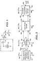
- FIG. 1 is a schematic diagram of an equivalent circuit of a standard voltage reference.
- the voltage reference 10 is represented by an ideal voltage source 12 connected in series to the voltage reference output impedance (Z o ) 14.
- the reference voltage supplied by the voltage reference (V REFIN ) is provided at the reference source output terminal 16.
- the output terminal 16 is connected to a load which, in this figure, is represented by a load resistor (Rd 18 and a load capacitor (C L ) 20.
- R L and C L 18 and 20 represent the resistance and capacitance of the bit lines and memory cells of an IC memory array.
- the disadvantages of high output impedance will now be described in this context.
- VREFIN will differ from V REF by a term equal to the magnitude of the current supplied multiplied by the magnitude of the output impedance Z o 14.
- V REFIN will not have a stable value, but will fluctuate in proportion to the current supplied by the voltage reference 10.
- the time to charge the load capacitor 20, C L depends on the sum of Z o , and R L 14 and 18 and is increased in proportion to the magnitude of the output impedance, Z o . Since, in this context, C L 20 represents the capacitance of the memory cells in a memory array, any increase in the time required to charge or discharge the capacitor, C L 20, slows down the access time of the memory, thereby decreasing its efficiency.
- FIG. 2 is a block diagram of the invention.
- the output terminal 16 of the high output impedance voltage reference 10 is connected to the input 30 of a CMOS preamplifier 32.
- the CMOS preamplifier 32 generates first and second output signals at the first and second amplifier outputs 34 and 36 which are coupled to the first and second input terminals 38 and 40 of an isolation stage 42.
- the isolation stage 42 generates first and second isolation stage output signals at first and second output terminals 44 and 46 which are coupled to the first and second input terminals 48 and 50 of a source follower output stage 52.
- the source follower output stage 52 generates an output signal at its output terminal 54.
- the high-output impedance voltage reference 10, the preamplifier 32, the isolation stage 42, and source follower 52 are each coupled to the V cc and ground terminals 56 and 58 of an external power supply (not shown).
- the CMOS preamplifier 32 is configured so that the virtually no current, 1 0 , flows into or out of the output terminal 16 of the high output impedance voltage reference 10. Thus, the above-described voltage fluctuations due to current flow through the output impedance is eliminated from the circuit.
- the isolation stage 42 protects the preamplifier 32 from the effects of a bump in the value of V cc and from output voltage fluctuations.
- the source follower output stage 52 provides a high output current and is characterized by an inherently low output impedance. The gain of the total system is approximately unity so that a stable V REFOUT equal in magnitude to V REF and a capability of providing a large driving current is realized by the system.
- the isolation stage is not included and the outputs 34 and 36 from the CMOS preamplifier 34 are connected directly to the inputs 48 and 50 of the source follower output stage 52.
- the system is designed to dissipate very low power when not providing driving current to an external load.
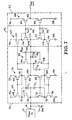
- FIG. 3 is a circuit diagram of an embodiment of the invention with the isolation stage 42 omitted.
- a first series circuit 60 between the V cc terminal 56 and ground terminals 58 includes four MOS transistors.
- the first circuit 60 includes a first PMOS transistor 68 with its source connected to the V cc terminal 56 and its drain connected to a first node 70.
- the first node 70 is coupled to the drain terminal of a second NMOS transistor 72 and is also coupled to the gate of second transistor 72 while the source terminal of second transistor 72 is coupled to a second node 73.
- the output terminal 16 of the high output impedance voltage reference 10 is coupled to the second node 73 of the first circuit 60.
- Second node 73 is coupled to the source terminal of a third PMOS transistor 74 with the drain terminal of third transistor 74 connected to a third node 76 and also with the gate of third transistor 74 connected to third node 76. Finally, the drain terminal of a fourth NMOS transistor 78 is connected to third node 76 while the source terminal is connected to the ground terminal 58 of the external power supply.
- the second transistor 72 is connected in a diode configuration.
- the voltage difference (V Ds ) between the drain and source (first node 70 and second node 73) of second transistor 72 is equal to the voltage difference (V GS ) between the gate and source (second node 73) because the gate is coupled to the drain.
- the second transistor 72 will conduct when V GS is equal to V TN (the threshold voltage of the second NMOS transistor 72).
- V DS is equal to V TN second transistor 72 conducts and holds the voltage at the first node 70, V(1), equal to V REFIN +V TN -
- V ( 3 ) is equal to V REF -V TP where V T p is the threshold voltage of third PMOS transistor 74.
- the preamplifier 32 further includes a second series circuit 79.
- a fifth PMOS transistor 80 has its source terminal coupled to V cc terminal 56 and its drain terminal coupled to a fourth node 81.
- the fourth node 81 is coupled to the gates of first and fifth transistors 68 and 80.
- the fourth node 81 is coupled to the drain terminal of a sixth NMOS transistor 82 with the drain of sixth transistor 82 connected to a fifth node 83.
- the gate of the sixth transistor 82 is coupled to the first node 70.
- the fifth node 83 is coupled to the source terminal of a seventh PMOS transistor 84 with the drain terminal of the seventh transistor 84 coupled to a sixth node 85.
- the gate of the seventh transistor 84 is coupled to the third node 76.
- the sixth node 85 is coupled to the drain terminal of an eighth NMOS transistor 86 with the source terminal of the eighth transistor 86 coupled to ground terminal 58.
- the sixth node 85 is coupled to the gates of the fourth and eighth transistor
- the characteristics of several MOS transistors fabricated on an IC may be closely matched if the various corresponding components of the matched transistors are formed during the same process step. For example, if all the drains are formed during a single ion implantation step any variations in the ion implantation rate would affect all the matched transistors equally. Thus, the threshold and gain characteristics of all the matched transistors would be nearly identical.
- the drain to source current, I os of an MOS transistor is dependent on the ratio of width to the length of the transistor channel.
- the first and fifth transistors 68 and 80, second and sixth transistors 72 and 82, third and seventh transistors 74 and 84, and fourth and eighth transistors 78 and 86 are matched transistor pairs.
- a third series circuit 88 connected between the V CC and ground terminals 56 and 58 functions as the source follower output stage 52 of Figure 2.
- the third series circuit 88 includes a ninth NMOS transistor 90 with its drain terminal connected to the V CC terminal 56 and its source terminal connected to a seventh node 92.
- the seventh node 92 is connected to the source terminal of a tenth PMOS transistor 94 having its drain terminal connected to the ground terminal 58.
- the gate of the ninth transistor 90 is connected to the first node 70 of the first circuit 60 and, thus, the gate voltage of ninth transistor 90 is equal to VREFIN+VTN' Similarly, the gate of the tenth transistor 94 is connected to the third circuit node 76 and the voltage at the gate of tenth transistor 94 is equal to V REFIN -V TP . Note that first and third nodes 70 and 76 correspond to the first and second preamplifier outputs (34 and 36 of Figure 2) and that the gates of ninth and tenth transistors 90 and 94 correspond to the source follower inputs (48 and 50 of Figure 2).
- the ninth and tenth transistors 90 and 94 are matched to the second and third transistors 72 and 74, respectively, in the first circuit 60 but W/L ratios are scaled up to provide high driving current at seventh node 92.
- Capacitor C o couples the second node 73 to the ground terminal 58; capacitor C 1 couples the V REFIN terminal 16 to the first node 70; capcaitor C 2 couples the V REFIN terminal 16 to the third node 76; capacitor C 3 couples the fifth node 83 to the ground terminal 58; capacitor C 4 couples the first node 70 to the ground terminal 58; and, capacitor C 5 couples the third node 76 to the ground terminal 58.
- a fourth series circuit 95 couples the fourth node 81 to the sixth node 85.
- the fourth series circuit 95 includes an eleventh NMOS transistor 96 with its drain terminal connected to fourth node 81 and its source terminal connected to an eighth node 97.
- Eighth node 97 is connected to the source terminal of a twelfth PMOS transistor 98.
- the drain of twelfth transistor 98 is connected to the sixth node 85.
- the gates of eleventh and twelfth transistors 96 and 98 are coupled to a ⁇ osc input 99.
- Capacitor C 6 couples the eighth node 97 to the ground terminal 58.
- I DS drain/ source current
- V Gs gate/ source voltage
- the first order dependence is depicted by the solid line 100a. Note that I DS is zero for V Gs less than V T and rises rapidly as V GS increases beyond V T .
- the second order dependence is depicted by the dotted line 100b. The scale of the dotted line is amplified to illustrate that the value of I DS is slightly greater than zero for V GS slightly less than V T .
- V GS is equal to or slightly less than V T
- V T is defined as the subthreshold region. Power dissipation in this region is very low because the value of l os is very small and power dissipation depends on (I DS ) 2 .
- V REFIN is equal to V cc /2.
- V(5) is also equal to V cc /2 for the reasons described below.
- the first, second, fifth, and sixth transistors 68, 72, 80 and 82 are connected to form a current mirror. If all the transistors had identical W/L ratios, then the current through the first and second circuits 60 and 79 would be equal for the following reasons.
- the V GS of the first and fifth transistors are both equal to +V T p because the gates of the fifth and first transistors 80 and 68 are coupled to the fourth node 81 and the sources of both transistors are coupled to the V cc terminal 56.
- the drain source current amplitudes, I DS (1) and l DS (5), through the first and fifth transistors 68 and 80 are both equal if the W/L ratios of the transistors are equal because the first and fifth transistors 68 and 80 are a matched transistor pair.
- V GS of the second and sixth transistors 72 and 82 are both equal to -V TN and the magnitudes of l DS (2) and l os (6) are equal.
- I DS (1) is equal to l DS (2) because the first and second transistors 68 and 72 are connected in series and l DS (5) and ) DS (6) are equal because the fifth and sixth transistors 80 and 82 are connected in series. The net result is that the current in both the first and second series circuits 60 and 79 is equal.
- the W/L ratios for the second and sixth transistors 72 and 82 are equal, but the ratio for the first transistor 68 is scaled down to a fraction, for example 1/4th, of the ratio for the fifth transistor 80. Accordingly, the value of The first and second transistors 68 and 72 are connected in series so that As described above, the second and sixth transistors 72 and 82 are matched transistors with the same W/L ratio and have the same V GS so that And, since fifth and sixth transistors 80 and 82 are connected in series,
- circuit of Figure 5 forms a feedback loop to keep decreasing the current in the current mirror until the transistors are biased in the subthreshold region.
- the voltage at the first node 70, V(1) is equal to V REF +V TNS where V TNS indicates that the second transistor 72 is biased in the subthreshold region.
- the voltage at the third node 76, V(3) is V REF ⁇ V TPS ⁇
- the voltages V(1) and V(3) are the output voltages of the preamplifier stage 32.
- the ninth and tenth transistors 90 and 94 of the source follower stage 52 are matched to the second and third transistors 72 and 74, respectively, but have increased W/L ratios to provide high driving current.
- V REFIN The magnitude of the voltage at the V REFOUT output terminal 92 is equal to V REFIN for the following reasons:
- V(3) The voltage at the third node 73, V(3), is equal to V REFIN for the same reasons.
- the ninth and tenth transistors 90 and 94 have their gates coupled to first node 70 and third node 76, respectively, and their sources coupled to V REFOUT terminal 92.
- matched second transistor 72 and ninth transistor 90 have the same V GS and are therefore both biased in the sub- threshold region. Accordingly, virtually no power is dissipated in the no load state due to the low value of the current flowing through the circuit in the subthreshold bias region.
- the source follower 52 provides high source/sink current drive due to the high W/L ratios of the ninth and tenth transistors 90 and 94.
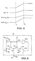
- FIG. 7 is a timing diagram depicting the magnitudes of V cc , V(4), and V(1). This graph is exemplary only and does not depict the actual time dependence of the various functions.
- V cc bumps from four volts to six volts, bumps from two volts to three volts, and the magnitudes of V TNS and V TPS are set equal to one.
- the V cc bump starts at time T, and ends at time T 2 .
- V cc bumps from four to six volts and V cc /2 bumps from two to three volts. Since the change in magnitude of V cc/ 2 is less than the change of magnitude in V cc the slope of the curve representing V cc /2 is less than the slope of the curve representing V cc . As described above, V(4) is equal to V cc -1 and, thus, V(4) increases at the same rate as V cc . The V cc bump increases the current in the fourth transistor 80, los(4), above the subthreshold level and charges the fourth node 81. This charging increases V(4) and turns off the first transistor 68.
- the resulting current flow through the first transistor 68, I DS (1), is so small that the first node 70 remains trapped at 3 volts, the original V cc /2+1.
- the fifth transistor 82 With V(1) at 3 volts and the fifth node 83 at 2 volts, the original V cc /2 value, the fifth transistor 82 remains biased in the subthreshold region.
- This small subthreshold current, l os (5) is insufficient to discharge the fourth node 81 and turn in the first transistor 68 to untrap the first node 70.
- the circuit depicted in Figure 3 includes two mechanisms for preventing charge build up at the fourth and sixth nodes 81 and 85 and the trapping of the first and third nodes 70 and 76.
- the first is a charge pump circuit formed by the fourth series circuit 95.
- the second mechanism is a capacitive coupling network formed by capacitors C1, C2, and C3.
- the eleventh transistor 96 transfers a small amount of charge between the fourth node 81 and capacitor C6 when the value of ⁇ osc goes high. This charge is then transferred from capacitor C6 to the sixth node 85 when the value of ⁇ osc goes low.
- the value of C6 is selected so that the average value of the current flowing through the charge pump circuit 95 is on the order of several nanoamps. Thus, the power dissipation of the overall circuit is not increased by the presence of the charge pump circuit 95.
- the capacitor C1 coupling the V REFIN terminal 16 to the first node 70
- C o coupling the fifth node 83 to the ground terminal 56
- the operation will be described for the case, set forth above, where the first node 70 is trapped at 3 volts during a V cc bump from 4 volts to 6 volts.
- V cc bumps from 4 to 6 volts V cc /2 bumps from 2 to 3 volts
- capacitor C 1 partially couples this V cc /2 voltage bump to the first node 70. Therefore, V(1) increases to 3 volts plus a small increment.
- the increase in V(1) increases the current through the sixth transistor 82 partially discharges the fourth node 81.
- the current through the sixth transistor 82 is sunk by the large capacitor C 3 .
- V(4) The reduction of charge on the fourth node 81 decreases V(4) from 5 volts to 5 volts minus a small increment. This decrease in V(4) increases the current through the first transistor 68 and charges the first node to a higher voltage. This increase in V(1) continues the feedback described above.
- the large capacitor C o settles the circuit and stops the feedback process when the nodes are at the correct voltage levels.
- the capacitors C 4 and C s decouple the first and third nodes 70 and 76 from the effects of output voltage bumps.
- a fifth series circuit 102 interconnects the preamplifier 32 to the source follower output stage 52.
- This third circuit 102 includes a thirteenth PMOS transistor 104 having its source terminal connected to V cc terminal 58 and its drain terminal connected to a ninth node 106. The gate of the thirteenth transistor 104 is coupled to the fourth node 81.
- a fourteenth NMOS transistor 108 has its drain terminal connected to the ninth node 106 and its source terminal connected to a tenth node 110. The fourteenth transistor 108 is connected in the diode configuration with its gate coupled to ninth node 106.
- a fifteenth PMOS transistor 112 has its source terminal connected to the tenth node 110 and its drain terminal connected to an eleventh node 114.
- the fifteenth transistor 112 is connected in the diode configuration with its gate coupled to the eleventh node 114.
- a sixteenth NMOS transistor 116 has its drain terminal coupled to the eleventh node 114 and its source terminal coupled to the ground terminal 58.
- the gate of the sixteenth transistor 116 is coupled to the sixth node 85. Note that positions of the first and second series circuits 60 and 79 in Figure 8 have been interchanged relative to their positions in Figure 3.
- the gates of the thirteenth and sixteenth transistors 104 and 116 correspond to the isolation stage inputs (38 and 40 of Figure 2) and the ninth and eleventh nodes 106 and 114 correspond to the isolation stage outputs (44 and 46 of Figure 2).
- the first and third nodes 70 and 76 correspond to the preamplifier outputs (34 and 36 of Figure 2).
- the thirteenth, fourteenth, fifteenth, and sixteenth transistors 104, 108, 112, and 116 in the isolation stage circuit 102 form matched pairs with the first, second, third, and fourth transistors 68, 72, 74, and 78 in the preamplifier 32. Additionally, the ninth and fourteenth transistors 90 and 108 and tenth and fifteenth transistors 94 and 114 form matched pairs. However, the W/L ratios of the thirteenth, fourteenth, fifteenth, and seventeenth transistors 104,108,112, and 116 are scaled up relative to the transistors in the preamplifier 32 so that more current flows in the isolation stage circuit 102.
- the W/L ratios in the transistors 90 and 94 in the source follower circuit 88 are scaled up from the transistors in the isolation stage 42.
- the magnitude of the voltage of the fifth and tenth coupled nodes 83 and 110 is equal to VREFIN for the reasons set forth above.
- the isolation stage series circuit 102 mirrors the first series circuit 79.
- the ninth and eleventh nodes 106 and 114 mirror the first and third nodes 70 and 76, respectively.
- the increased scale of the W/L ratios of the transistors in the fifth series circuit 102 provide increased current to charge the ninth and eleventh nodes 106 and 114 and to diminish the effects of V cc bump and output bounce on the circuit.
- FIG. 8 is a circuit diagram of an exemplary high output impedance voltage reference suitable for use with the present system.
- a PMOS transistor 120 has its source terminal connected to the V cc terminal 56 and its drain terminal connected to node 122. Capacitor C 7 is connected between node 122 and the ground terminal 58.
- An NMOS transistor 124 has its drain terminal-connected to node 122 and its source terminal connected to node 126 and an NMOS transistor 128 has its source terminal connected to node 126 and its drain terminal connected to node 130. Capacitor C 8 is connected between node 130 and the ground terminal 58.
- An NMOS transistor 132 has its drain terminal connected to node 130 and its source terminal connected to ground terminal 58.
- An inverter 134 has its input connected to node 136 and its output connected to the gate of transistor 132. The gates of transistors 120,124, and 128 are connected to node 136.
- a periodic clock signal, ⁇ that alternates between 0 and V cc is applied to node 136.
- the clock signal amplitude is equal to V cc
- transistors 120 and 132 are on and transistors 124 and 128 are off.
- capacitor C 7 charges to +V cc through transistor 120 and capacitor C 8 discharges to ground through transistor 132.
- transistors 120 and 132 are turned off and transistors 124 and 128 are on.
- node 126 is coupled to capacitor C 7 and C s .
- the values of C 7 and C a are set equal so that the sum of the voltages at node 126 is equal to V cc /2.
- Node 126 is coupled to the output terminal 16 of the high output impedance voltage reference 10.
- subthreshold biasing was accomplished by scaling the W/L ratios of specified transistors.
- these W/L ratios may be arbitrarily scaled as long as the feedback reduces the current.
- V REFIN was set equal V cc /2, however, V REFIN may assume any value between the absolute value of V T p and V CC -V TN .
- charge transfer circuit need not be a charge pump but circuit could be a large resistor.
Landscapes
- Engineering & Computer Science (AREA)
- Power Engineering (AREA)
- Microelectronics & Electronic Packaging (AREA)
- Physics & Mathematics (AREA)
- Radar, Positioning & Navigation (AREA)
- General Physics & Mathematics (AREA)
- Electromagnetism (AREA)
- Automation & Control Theory (AREA)
- Nonlinear Science (AREA)
- Logic Circuits (AREA)
- Control Of Electrical Variables (AREA)
- Amplifiers (AREA)
- Dram (AREA)
Claims (19)
lesdits moyens destinés à empêcher le piégeage comprennent:
Priority Applications (1)
| Application Number | Priority Date | Filing Date | Title |
|---|---|---|---|
| AT86301221T ATE49815T1 (de) | 1985-03-04 | 1986-02-20 | Niederleistungs-cmos-referenzgenerator mit treiber mit niedriger impedanz. |
Applications Claiming Priority (2)
| Application Number | Priority Date | Filing Date | Title |
|---|---|---|---|
| US06/707,726 US4634894A (en) | 1985-03-04 | 1985-03-04 | Low power CMOS reference generator with low impedance driver |
| US707726 | 1991-05-30 |
Publications (2)
| Publication Number | Publication Date |
|---|---|
| EP0195525A1 EP0195525A1 (fr) | 1986-09-24 |
| EP0195525B1 true EP0195525B1 (fr) | 1990-01-24 |
Family
ID=24842912
Family Applications (1)
| Application Number | Title | Priority Date | Filing Date |
|---|---|---|---|
| EP86301221A Expired - Lifetime EP0195525B1 (fr) | 1985-03-04 | 1986-02-20 | Générateur de référence CMOS de faible puissance comportant un étage de sortie à faible impédance |
Country Status (5)
| Country | Link |
|---|---|
| US (1) | US4634894A (fr) |
| EP (1) | EP0195525B1 (fr) |
| JP (1) | JPH0789303B2 (fr) |
| AT (1) | ATE49815T1 (fr) |
| DE (1) | DE3668509D1 (fr) |
Families Citing this family (39)
| Publication number | Priority date | Publication date | Assignee | Title |
|---|---|---|---|---|
| US4788455A (en) * | 1985-08-09 | 1988-11-29 | Mitsubishi Denki Kabushiki Kaisha | CMOS reference voltage generator employing separate reference circuits for each output transistor |
| IT1186108B (it) * | 1985-11-27 | 1987-11-18 | Sgs Microelettronica Spa | Circuito ripetitore di tensione a basso offset |
| US4758743A (en) * | 1986-09-26 | 1988-07-19 | Motorola, Inc. | Output buffer with improved di/dt |
| US4818901A (en) * | 1987-07-20 | 1989-04-04 | Harris Corporation | Controlled switching CMOS output buffer |
| JPH0198007A (ja) * | 1987-10-09 | 1989-04-17 | Nec Corp | 電源回路 |
| US4825099A (en) * | 1987-12-04 | 1989-04-25 | Ford Microelectronics | Feedback-controlled current output driver having reduced current surge |
| US4933572A (en) * | 1988-03-17 | 1990-06-12 | Precision Monolithics, Inc. | Dual mode voltage reference circuit and method |
| US5687109A (en) * | 1988-05-31 | 1997-11-11 | Micron Technology, Inc. | Integrated circuit module having on-chip surge capacitors |
| US6124625A (en) * | 1988-05-31 | 2000-09-26 | Micron Technology, Inc. | Chip decoupling capacitor |
| JP2752640B2 (ja) * | 1988-08-07 | 1998-05-18 | 日本電気アイシーマイコンシステム株式会社 | 中間レベル発生回路 |
| ATE99434T1 (de) * | 1989-03-06 | 1994-01-15 | Siemens Ag | Integrierte referenzspannungsquelle. |
| US4994891A (en) * | 1989-06-20 | 1991-02-19 | Advanced Micro Devices | Shielded transistor device |
| US5099156A (en) * | 1990-10-02 | 1992-03-24 | California Institute Of Technology | Subthreshold MOS circuits for correlating analog input voltages |
| DE4041761A1 (de) * | 1990-12-24 | 1992-06-25 | Standard Elektrik Lorenz Ag | Stromsenke |
| US5302888A (en) * | 1992-04-01 | 1994-04-12 | Texas Instruments Incorporated | CMOS integrated mid-supply voltage generator |
| US5362988A (en) * | 1992-05-01 | 1994-11-08 | Texas Instruments Incorporated | Local mid-rail generator circuit |
| JP2814905B2 (ja) * | 1993-12-28 | 1998-10-27 | 日本電気株式会社 | ドライバ/レシーバ回路 |
| JP3626521B2 (ja) * | 1994-02-28 | 2005-03-09 | 三菱電機株式会社 | 基準電位発生回路、電位検出回路および半導体集積回路装置 |
| JPH10500823A (ja) * | 1994-05-19 | 1998-01-20 | ポラロイド コーポレイション | アクティブ画素を有するcmos撮像アレイ |
| KR970005570B1 (ko) * | 1994-07-14 | 1997-04-17 | 현대전자산업 주식회사 | 데이타 출력버퍼 |
| JP3592423B2 (ja) * | 1996-01-26 | 2004-11-24 | 株式会社ルネサステクノロジ | 半導体集積回路装置 |
| US5793223A (en) * | 1996-08-26 | 1998-08-11 | International Business Machines Corporation | Reference signal generation in a switched current source transmission line driver/receiver system |
| US5815107A (en) * | 1996-12-19 | 1998-09-29 | International Business Machines Corporation | Current source referenced high speed analog to digitial converter |
| US5923276A (en) * | 1996-12-19 | 1999-07-13 | International Business Machines Corporation | Current source based multilevel bus driver and converter |
| JPH10260741A (ja) | 1997-03-17 | 1998-09-29 | Oki Electric Ind Co Ltd | 定電圧発生回路 |
| US6066971A (en) * | 1997-10-02 | 2000-05-23 | Motorola, Inc. | Integrated circuit having buffering circuitry with slew rate control |
| US6037811A (en) * | 1997-10-10 | 2000-03-14 | International Microcircuits, Inc. | Current-controlled output buffer |
| EP1105968A4 (fr) * | 1998-06-15 | 2005-06-15 | Internat Microcircuits Inc | Tampon de sortie commande par courant |
| US6819183B1 (en) * | 2003-05-23 | 2004-11-16 | Qualcomm, Incorporated | Temperature and process compensation of MOSFET operating in sub-threshold mode |
| US6856177B1 (en) * | 2003-07-22 | 2005-02-15 | International Rectifier Corporation | High side power switch with charge pump and bootstrap capacitor |
| DE102006041000A1 (de) * | 2006-08-31 | 2008-03-20 | Qimonda Ag | Anordnung und Verfahren zum Lesen einer Speicherzelle eines Halbleiterspeichers |
| DE102007036580A1 (de) * | 2007-08-02 | 2009-02-05 | Endress + Hauser Flowtec Ag | Feldbuseinheit für einen Zwei-Leiter-Feldbus |
| US8004350B2 (en) | 2009-06-03 | 2011-08-23 | Infineon Technologies Ag | Impedance transformation with transistor circuits |
| US20110316505A1 (en) * | 2010-06-23 | 2011-12-29 | Texas Instruments Incorporated | Output Buffer With Improved Output Signal Quality |
| CN102520757B (zh) * | 2011-12-28 | 2013-11-27 | 南京邮电大学 | 一种灌电流和拉电流产生电路 |
| TWI645279B (zh) * | 2016-11-15 | 2018-12-21 | 瑞昱半導體股份有限公司 | 參考電壓緩衝電路 |
| US11024373B2 (en) | 2019-09-12 | 2021-06-01 | Hefei Reliance Memory Limited | Voltage-mode bit line precharge for random-access memory cells |
| CN113282128B (zh) * | 2021-04-20 | 2022-04-22 | 珠海博雅科技股份有限公司 | 亚阈值基准电压源电路、电路板及基准电压源 |
| CN113296571B (zh) * | 2021-07-27 | 2021-10-22 | 上海南麟集成电路有限公司 | 基准电压源电路 |
Family Cites Families (8)
| Publication number | Priority date | Publication date | Assignee | Title |
|---|---|---|---|---|
| US4061962A (en) * | 1976-06-11 | 1977-12-06 | Rca Corporation | Current mirror amplifier augumentation of regulator transistor current flow |
| US4264874A (en) * | 1978-01-25 | 1981-04-28 | Harris Corporation | Low voltage CMOS amplifier |
| US4201947A (en) * | 1978-02-10 | 1980-05-06 | Rca Corporation | Long-tailed-pair connections of MOSFET's operated in sub-threshold region |
| FR2447610A1 (fr) * | 1979-01-26 | 1980-08-22 | Commissariat Energie Atomique | Generateur de tension de reference et circuit de mesure de la tension de seuil d'un transistor mos, applicable a ce generateur de tension de reference |
| JPS57155628A (en) * | 1981-03-23 | 1982-09-25 | Hitachi Ltd | Generating circuit of reference voltage |
| JPS57157315A (en) * | 1981-03-24 | 1982-09-28 | Nec Corp | Intermediate voltage generating circuit |
| US4453094A (en) * | 1982-06-30 | 1984-06-05 | General Electric Company | Threshold amplifier for IC fabrication using CMOS technology |
| US4595844A (en) * | 1984-01-16 | 1986-06-17 | Itt Corporation | CMOS high current output driver |
-
1985
- 1985-03-04 US US06/707,726 patent/US4634894A/en not_active Expired - Lifetime
-
1986
- 1986-02-20 AT AT86301221T patent/ATE49815T1/de not_active IP Right Cessation
- 1986-02-20 EP EP86301221A patent/EP0195525B1/fr not_active Expired - Lifetime
- 1986-02-20 DE DE8686301221T patent/DE3668509D1/de not_active Expired - Lifetime
- 1986-03-03 JP JP61047157A patent/JPH0789303B2/ja not_active Expired - Fee Related
Also Published As
| Publication number | Publication date |
|---|---|
| EP0195525A1 (fr) | 1986-09-24 |
| US4634894A (en) | 1987-01-06 |
| JPH0789303B2 (ja) | 1995-09-27 |
| JPS61217815A (ja) | 1986-09-27 |
| DE3668509D1 (de) | 1990-03-01 |
| ATE49815T1 (de) | 1990-02-15 |
Similar Documents
| Publication | Publication Date | Title |
|---|---|---|
| EP0195525B1 (fr) | Générateur de référence CMOS de faible puissance comportant un étage de sortie à faible impédance | |
| US5808506A (en) | MOS charge pump generation and regulation method and apparatus | |
| US5039877A (en) | Low current substrate bias generator | |
| US6456154B2 (en) | Drive control circuit of charged pump circuit | |
| US5162668A (en) | Small dropout on-chip voltage regulators with boosted power supply | |
| US5808505A (en) | Substrate biasing circuit having controllable ring oscillator | |
| US5339236A (en) | Charge pump circuit for intermediate voltage between power supply voltage and its double voltage | |
| US6249169B1 (en) | Transistor output circuit | |
| US4930112A (en) | Semiconductor device having a voltage limiter | |
| US4115710A (en) | Substrate bias for MOS integrated circuit | |
| US5892390A (en) | Internal power supply circuit with low power consumption | |
| US4463270A (en) | MOS Comparator circuit | |
| US6215159B1 (en) | Semiconductor integrated circuit device | |
| US5801569A (en) | Output driver for mixed supply voltage systems | |
| EP0451870B1 (fr) | Circuit de génération d'une tension de référence | |
| US5929679A (en) | Voltage monitoring circuit capable of reducing power dissipation | |
| JPH06217527A (ja) | 高効率nチャネルチャージポンプ | |
| EP0638984A1 (fr) | Pompe de charge à basse tension | |
| US5973544A (en) | Intermediate potential generation circuit | |
| US5278798A (en) | Semiconductor memory device | |
| JPH07240472A (ja) | 絶縁破壊強度の増加されたcmos回路 | |
| US5633604A (en) | Mixed mode output buffer circuit for CMOSIC | |
| JPS61222318A (ja) | パワ−オンリセツト回路 | |
| US20050083106A1 (en) | Analog voltage distribution on a die using switched capacitors | |
| US6670845B1 (en) | High D.C. voltage to low D.C. voltage circuit converter |
Legal Events
| Date | Code | Title | Description |
|---|---|---|---|
| PUAI | Public reference made under article 153(3) epc to a published international application that has entered the european phase |
Free format text: ORIGINAL CODE: 0009012 |
|
| AK | Designated contracting states |
Kind code of ref document: A1 Designated state(s): AT BE CH DE FR GB IT LI LU NL SE |
|
| 17P | Request for examination filed |
Effective date: 19861003 |
|
| 17Q | First examination report despatched |
Effective date: 19871216 |
|
| GRAA | (expected) grant |
Free format text: ORIGINAL CODE: 0009210 |
|
| AK | Designated contracting states |
Kind code of ref document: B1 Designated state(s): AT BE CH DE FR GB IT LI LU NL SE |
|
| PG25 | Lapsed in a contracting state [announced via postgrant information from national office to epo] |
Ref country code: IT Free format text: LAPSE BECAUSE OF FAILURE TO SUBMIT A TRANSLATION OF THE DESCRIPTION OR TO PAY THE FEE WITHIN THE PRESCRIBED TIME-LIMIT;WARNING: LAPSES OF ITALIAN PATENTS WITH EFFECTIVE DATE BEFORE 2007 MAY HAVE OCCURRED AT ANY TIME BEFORE 2007. THE CORRECT EFFECTIVE DATE MAY BE DIFFERENT FROM THE ONE RECORDED. Effective date: 19900124 Ref country code: FR Effective date: 19900124 Ref country code: LI Effective date: 19900124 Ref country code: NL Effective date: 19900124 Ref country code: BE Effective date: 19900124 Ref country code: SE Effective date: 19900124 Ref country code: CH Effective date: 19900124 Ref country code: AT Effective date: 19900124 |
|
| REF | Corresponds to: |
Ref document number: 49815 Country of ref document: AT Date of ref document: 19900215 Kind code of ref document: T |
|
| PG25 | Lapsed in a contracting state [announced via postgrant information from national office to epo] |
Ref country code: LU Free format text: LAPSE BECAUSE OF NON-PAYMENT OF DUE FEES Effective date: 19900228 |
|
| REF | Corresponds to: |
Ref document number: 3668509 Country of ref document: DE Date of ref document: 19900301 |
|
| PG25 | Lapsed in a contracting state [announced via postgrant information from national office to epo] |
Ref country code: GB Effective date: 19900324 |
|
| REG | Reference to a national code |
Ref country code: CH Ref legal event code: PL |
|
| EN | Fr: translation not filed | ||
| NLV1 | Nl: lapsed or annulled due to failure to fulfill the requirements of art. 29p and 29m of the patents act | ||
| PG25 | Lapsed in a contracting state [announced via postgrant information from national office to epo] |
Ref country code: DE Effective date: 19901101 |
|
| PLBE | No opposition filed within time limit |
Free format text: ORIGINAL CODE: 0009261 |
|
| STAA | Information on the status of an ep patent application or granted ep patent |
Free format text: STATUS: NO OPPOSITION FILED WITHIN TIME LIMIT |
|
| GBPC | Gb: european patent ceased through non-payment of renewal fee | ||
| 26N | No opposition filed |