EP0196391A2 - Integrierte Schaltung mit einem Gallium-Arsenid-Gate-Array unter Verwendung von NAND-Gattern in direkt gekoppelter Feldeffekttransistorlogik - Google Patents
Integrierte Schaltung mit einem Gallium-Arsenid-Gate-Array unter Verwendung von NAND-Gattern in direkt gekoppelter Feldeffekttransistorlogik Download PDFInfo
- Publication number
- EP0196391A2 EP0196391A2 EP85309059A EP85309059A EP0196391A2 EP 0196391 A2 EP0196391 A2 EP 0196391A2 EP 85309059 A EP85309059 A EP 85309059A EP 85309059 A EP85309059 A EP 85309059A EP 0196391 A2 EP0196391 A2 EP 0196391A2
- Authority
- EP
- European Patent Office
- Prior art keywords
- normally
- transistor
- field effect
- type field
- gate
- Prior art date
- Legal status (The legal status is an assumption and is not a legal conclusion. Google has not performed a legal analysis and makes no representation as to the accuracy of the status listed.)
- Granted
Links
Images


Classifications
-
- H—ELECTRICITY
- H03—ELECTRONIC CIRCUITRY
- H03K—PULSE TECHNIQUE
- H03K19/00—Logic circuits, i.e. having at least two inputs acting on one output; Inverting circuits
- H03K19/01—Modifications for accelerating switching
- H03K19/017—Modifications for accelerating switching in field-effect transistor circuits
- H03K19/01707—Modifications for accelerating switching in field-effect transistor circuits in asynchronous circuits
-
- H—ELECTRICITY
- H03—ELECTRONIC CIRCUITRY
- H03K—PULSE TECHNIQUE
- H03K19/00—Logic circuits, i.e. having at least two inputs acting on one output; Inverting circuits
- H03K19/02—Logic circuits, i.e. having at least two inputs acting on one output; Inverting circuits using specified components
- H03K19/08—Logic circuits, i.e. having at least two inputs acting on one output; Inverting circuits using specified components using semiconductor devices
- H03K19/094—Logic circuits, i.e. having at least two inputs acting on one output; Inverting circuits using specified components using semiconductor devices using field-effect transistors
- H03K19/0952—Logic circuits, i.e. having at least two inputs acting on one output; Inverting circuits using specified components using semiconductor devices using field-effect transistors using Schottky type FET MESFET
Definitions
- the present invention generally relates to a gate array integrated circuit and, more particularly, to a gallium arsenide (GaAs) gate array integrated circuit employing direct-coupled field effect transistor logic gates (DCFL).
- GaAs gallium arsenide
- DCFL direct-coupled field effect transistor logic gates
- a buffered FET Logic (referred to as "BFL"), Schottky Diode FET Logic (referred to as “SDFL”) and direct-coupled FET Logic (referred to as “DCFL”), etc. are known in the art.
- a NAND gate, NOR gate and INVERTER are constituted by either normally-on type FET's (referred to as “D-FET”), or normally-off type FET's (referred to as "E-FET”).
- D-FET normally-on type FET's
- E-FET normally-off type FET's
- BFL consumes several milliwatts (mW) to several tens of mW and SDFL consumes 1 mW to several mW, while DCFL consumes only several hundred microwatts (uW) per gate.
- mW milliwatts
- uW microwatts
- a MOS-FET such as in a silicon integrated circuit
- FET is restricted to a junction type FET (a pn junction or a Schottky junction type).
- the Schottky junction type is used from the standpoint of the high-speed operation and fine construction requirements.
- a DCFL using the Schottky junction type FET's is operated in such a mode as to apply a forward bias across the gate and source of a driver FET, a high logic level is clamped at a forward raising voltage level on the Schottky junction.
- a logical level of typical DCFL is as small as about 0.6 V and a typical noise margin thereof is as small as about 0.2 V.
- Fig. 1 is one form of such a circuit arrangement.
- the driver FET 63 on the ground line side is in an ON state, the source voltage of the driver FET 62 on the load side is further increased by a voltage drop defined by the series resistance times the source-to-drain current.
- This series resistance is the resistance of the source-to-drain path of the driver FET when turned on.
- a noise margin on the low level side becomes very small and stable operation for the NAND gate can be hardly expected.
- NOR gate circuit is mainly constructed by a load FET 71 and a parallel circuit of two driver FET's 72 and 73 as shown in Fig. 2.
- the NAND circuit can be comprised of a combination of a NOR gate and inverter.
- an occupation area in the whole IC pattern due to the use of two logic stages of gates (and thus an increased number of gates) is increased, as well as an operation time is delayed and thus a NAND gate of a single stage configuration is required. Since in the gate array integrated circuit the size and pattern of its basic cell are previously determined, it is undesirable from the standpoint of the wafer availability to prepare various sizes of FET's, resulting in impairing its inherent excellent characteristics.
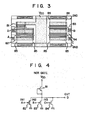
- Fig. 3 shows one pattern of a basic cell layout of a GaAs gate array of a typical DCFL (as disclosed in IEEE JOURNAL OF SOLID-STATE CIRCUITS, VOL. SC-19, No. 5 October, 1984 "A lK-Gate GaAs Gate Array" by Y. Ikawa et al. Fig. 7a).
- the basic cell 81 shows a D-FET serving as a load
- 82, 83 and 84 show E-FETs working as a driver.
- Connecting E-FETs 82, 83 and 84 in parallel configuration with the use of such a basic cell provides a 3-input NOR gate as shown in Fig. 4.
- the respective FETs 82, 83 and 84 are connected to the ground line "GND" as indicated by a broken line 85.
- a primary object of this invention is to provide a GaAs gate array integrated circuit which permits the use of a stably operated NAND gate employing an optimally integrable DCFL and the full use of a basic cell in view of the entire wafer area.
- Another object of this invention is to provide a GaAs gate array integrated circuit comprised of NAND gates having a lower signal delay.
- a gallium arsenide gate array integrated circuit comprising a plurality of direct-coupled field effect transistor logic gates connected between a power source and a ground potential, which logic gates including:
- This NAND gate 100 is preferably used in a GaAs gate array integrated circuit (not shown in detail).
- the NAND gate 100 includes a load FET 20 of a normally-on type (D-FET), a first driver FET 22 of a normally-off type (E-FET) and a second driver FET 24 consisting of parallel-connected FET's 24A and 24B.
- a source-to-drain current path of the load FET 20 is connected in series to those of the first and second FET's 22 and 24.
- An output terminal "C" is provided on a junction between the load FET 20 and the first driver FET 22.
- the first driver FET 22 has a gate electrode as a first input terminal "IN l ".
- the second driver FET's 24A and 24B are of the normally-off type (E-FET), gate electrodes of which are commonly connected so as to provide a second input terminal "IN 2 ".
- the sources of both FET's 24A and 24B are commonly grounded.
- FIG. 6 a layout is shown for such a NAND gate 100 of Fig. 5.
- a basic cell of Fig. 6 is exactly the same as that of Fig. 3 except for a wire connection. That is, the basic cell is constituted by a single D-FET 20 and three E-FET's 22, 24A and 24B.
- the D -FET 20 is provided as a load FET
- the first E-FET 22 is connected as a first driver FET in series with the load FET 20
- the second E-FET 24A and the third E - F ET 24B are connected in parallel to each other and in series with the first driver FET 22 so as to constitute a second driver FET 24.
- an electronic conductor 25 is used to bridge the first driver FET 22 and the second E-FET 24A of the second driver FET 24, and conductors 27 are employed to connect the second E-FET 24A and third E-FET 24B to the ground lines 28 and 29.
- a complete NAND gate 100 can be assembled by using only one basic cell as shown in Fig. 6.
- the turn-on resistance of the second driver FET 24 on the ground side becomes equivalently lower and the high level of the driver FET 22 at the first input IN 1 is set to maintain a noise margin of about 0.2 V, thus implementing a NAND gate 100 assuring its stable operation.
- the 2-input NAND gate 100 has been explained as having a cascade-connected array of two driver FETs as the logic gate
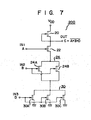
- this invention can effectively, equally applied to a 3-input NAND gate 200 (see Fig. 7) with, for example, a cascade-connected array of three driver FET's as the logic gate.
- the driver FET arrangement may comprise one FET at a load side, an intermediate parallel array of two FET's and a parallel circuit of three FET's at the ground side. This specific arrangement can be implemented with the use of such two basic cells as employed in the above-mentioned embodiment, if use is made of this type of basic cell.
- Fig. 7 is a circuit diagram showing the above-mentioned 3-input NAND gate 200 according to a second embodiment of this invention.
- the same reference numerals are employed to designate the same or similar elements shown in the first embodiment. Since the arrangement of the second embodiment is similar to that of the first embodiment with respect to a circuit portion including the load FET 20 to the second input IN 2 , only the remaining portion of the second embodiment will be explained below.
- a parallel circuit arrangement of three E-FET's 30A, 30B and 30C is connected, as a third driver FET 30, in series with the second driver FET 24. Commonly connected gates of the E-FETs 30A, 30B and 30C function as a third input IN 3 . In this way, it is possible to provide the 3-input NAND gate 200.
- This NAND gate 200 can implement the same noise margin and high-speed operation characteristics as those of the above-mentioned 2-input NAND gate 100.
- the second driver FET 24 includes the parallel circuit of E-FET's 24A and 24B
- the third driver FET 30 at the ground side includes the parallel circuit of three E-FET's 30A to 30C.
- the reason for this specific arrangement is that it is possible to improve the noise margin by making the parallel resistance (that is, the turn-on resistance) of the driver FET at the ground side as low as possible.
- FIG. 8 Referring to a layout and an actual circuit arrangement of the 3-input NAND gate 200 shown in Figs. 8 and 9, the above-described features of this second embodiment may be easily understood.
- through holes denoted by numeral 90 are formed between the first and second layers 92 and 94.
- the first layers 92 are indicated by dotted areas and the second layers 94 are denoted by hatched area in the drawing of Fig. 8.
- a plurality of E - FET's are connected in a parallel circuit arrangement so as to function as a single equivalent driver FET and thus the GaAs gate array can perform a stable logical operation with a smaller turn-on resistance and a smaller logical amplitude with DCFL as a basic cell. Furthermore, it is possible to constitute a NAND gate using the basic cell of a DCFL type including a plurality of E-FET's of the same size, and thus it is possible to implement a highly integrated gate array with a very effective cell area.
Landscapes
- Engineering & Computer Science (AREA)
- Physics & Mathematics (AREA)
- Computer Hardware Design (AREA)
- Computing Systems (AREA)
- General Engineering & Computer Science (AREA)
- Mathematical Physics (AREA)
- Power Engineering (AREA)
- Logic Circuits (AREA)
- Design And Manufacture Of Integrated Circuits (AREA)
- Bipolar Integrated Circuits (AREA)
- Junction Field-Effect Transistors (AREA)
Applications Claiming Priority (2)
| Application Number | Priority Date | Filing Date | Title |
|---|---|---|---|
| JP60064424A JPS61222250A (ja) | 1985-03-28 | 1985-03-28 | GaAsゲ−トアレイ集積回路 |
| JP64424/85 | 1985-03-28 |
Publications (3)
| Publication Number | Publication Date |
|---|---|
| EP0196391A2 true EP0196391A2 (de) | 1986-10-08 |
| EP0196391A3 EP0196391A3 (en) | 1987-04-08 |
| EP0196391B1 EP0196391B1 (de) | 1991-03-13 |
Family
ID=13257881
Family Applications (1)
| Application Number | Title | Priority Date | Filing Date |
|---|---|---|---|
| EP85309059A Expired EP0196391B1 (de) | 1985-03-28 | 1985-12-12 | Integrierte Schaltung mit einem Gallium-Arsenid-Gate-Array unter Verwendung von NAND-Gattern in direkt gekoppelter Feldeffekttransistorlogik |
Country Status (4)
| Country | Link |
|---|---|
| US (1) | US4639621A (de) |
| EP (1) | EP0196391B1 (de) |
| JP (1) | JPS61222250A (de) |
| DE (1) | DE3582160D1 (de) |
Cited By (1)
| Publication number | Priority date | Publication date | Assignee | Title |
|---|---|---|---|---|
| EP0356108A3 (de) * | 1988-08-23 | 1990-10-31 | AT&T Corp. | Sourcefolger-Feldeffektlogik (SFFL), geeignet für III-V Technologien |
Families Citing this family (8)
| Publication number | Priority date | Publication date | Assignee | Title |
|---|---|---|---|---|
| FR2589019B1 (fr) * | 1985-10-18 | 1991-04-12 | Thomson Csf | Porte logique a coincidence, triplet de portes logiques et circuit logique sequentiel mettant en oeuvre cette porte logique |
| US4965863A (en) * | 1987-10-02 | 1990-10-23 | Cray Computer Corporation | Gallium arsenide depletion made MESFIT logic cell |
| US4931670A (en) * | 1988-12-14 | 1990-06-05 | American Telephone And Telegraph Company | TTL and CMOS logic compatible GAAS logic family |
| JPH0548431A (ja) * | 1991-08-20 | 1993-02-26 | Fujitsu Ltd | 論理回路 |
| JP3196301B2 (ja) * | 1992-02-28 | 2001-08-06 | ソニー株式会社 | 化合物半導体集積回路装置 |
| JP3897826B2 (ja) * | 1994-08-19 | 2007-03-28 | 株式会社半導体エネルギー研究所 | アクティブマトリクス型の表示装置 |
| SG115733A1 (en) * | 2004-03-12 | 2005-10-28 | Semiconductor Energy Lab | Thin film transistor, semiconductor device, and method for manufacturing the same |
| JP7455604B2 (ja) * | 2020-02-14 | 2024-03-26 | 株式会社東芝 | ノーマリオン型トランジスタの駆動回路及び駆動方法 |
Family Cites Families (3)
| Publication number | Priority date | Publication date | Assignee | Title |
|---|---|---|---|---|
| FR2264434B1 (de) * | 1974-03-12 | 1976-07-16 | Thomson Csf | |
| US4300064A (en) * | 1979-02-12 | 1981-11-10 | Rockwell International Corporation | Schottky diode FET logic integrated circuit |
| US4430583A (en) * | 1981-10-30 | 1984-02-07 | Bell Telephone Laboratories, Incorporated | Apparatus for increasing the speed of a circuit having a string of IGFETs |
-
1985
- 1985-03-28 JP JP60064424A patent/JPS61222250A/ja active Pending
- 1985-12-05 US US06/804,744 patent/US4639621A/en not_active Expired - Lifetime
- 1985-12-12 DE DE8585309059T patent/DE3582160D1/de not_active Expired - Lifetime
- 1985-12-12 EP EP85309059A patent/EP0196391B1/de not_active Expired
Non-Patent Citations (3)
| Title |
|---|
| IEEE JOURNAL OF SOLID-STATE CIRCUITS, vol. SC-14, no. 2, April 1979, pages 221-239, New York, US; R.C. EDEN et al.: "The prospects for ultrahigh-speed VLSI GaAs digital logic" * |
| IEEE JOURNAL OF SOLID-STATE CIRCUITS, vol. SC-19, no. 5, October 1984, pages 721-728, New York, US; Y. IKAWA et al.: "A 1K-gate GaAs gate array" * |
| IEEE TRANSACTIONS ON ELECTRON DEVICES, vol. ED-25, no. 6, June 1978, pages 628-639; R. ZULEEG et al.: "Femtojoule high-speed planar GaAs E-JFET logic" * |
Cited By (1)
| Publication number | Priority date | Publication date | Assignee | Title |
|---|---|---|---|---|
| EP0356108A3 (de) * | 1988-08-23 | 1990-10-31 | AT&T Corp. | Sourcefolger-Feldeffektlogik (SFFL), geeignet für III-V Technologien |
Also Published As
| Publication number | Publication date |
|---|---|
| JPS61222250A (ja) | 1986-10-02 |
| EP0196391A3 (en) | 1987-04-08 |
| DE3582160D1 (de) | 1991-04-18 |
| EP0196391B1 (de) | 1991-03-13 |
| US4639621A (en) | 1987-01-27 |
Similar Documents
| Publication | Publication Date | Title |
|---|---|---|
| US4280065A (en) | Tri-state type driver circuit | |
| EP0145004B1 (de) | Kombinierte Bipolartransistor-Feldeffekttransistor-Schaltung | |
| EP0543426A1 (de) | Gateschaltung mit Feldeffekt- und Bipolartransistoren | |
| EP0239059B1 (de) | Logische Schaltung | |
| US4808851A (en) | ECL-compatible semiconductor device having a prediffused gate array | |
| EP0196391B1 (de) | Integrierte Schaltung mit einem Gallium-Arsenid-Gate-Array unter Verwendung von NAND-Gattern in direkt gekoppelter Feldeffekttransistorlogik | |
| EP0459422A2 (de) | Ausgangsdatenschaltung einer Halbleiteranordnung | |
| US4518871A (en) | Ga/As NOR/NAND gate circuit using enhancement mode FET's | |
| JPS61251228A (ja) | 複数入力論理集積回路 | |
| EP0562719B1 (de) | Integriertes Schaltkreisbauelement, gebildet aus einem Verbindungshalbleiter | |
| EP0110916B1 (de) | Logische schaltung mit stromgesteuerten anreicherungsfeldeffekttransistoren | |
| US4868422A (en) | TTL compatible CMOS logic circuit for driving heavy capacitive loads at high speed | |
| KR100241201B1 (ko) | 버스홀드회로 | |
| EP0242523A2 (de) | Integrierte Steuerungsstufe für logische FET-Schaltung | |
| EP0356108A2 (de) | Sourcefolger-Feldeffektlogik (SFFL), geeignet für III-V Technologien | |
| JPH01300714A (ja) | 負荷電流制御型論理回路 | |
| KR930009151B1 (ko) | 화합물 반도체 논리회로와 바이폴라 트랜지스터회로 사이에 설치된 인터페이스 회로 | |
| JPS5979641A (ja) | 半導体集積回路装置 | |
| US5309043A (en) | Compound logic circuit having NAND and NOR gate outputs and two transistors connected within both gate circuits | |
| JPH10257671A (ja) | 電子回路装置 | |
| JPH02280413A (ja) | 基本論理回路 | |
| EP0170134B1 (de) | Schottky-Dioden und Feldeffekt-Transistoren verwendende Logikschaltung | |
| US3965367A (en) | Multiple output logic circuits | |
| JPS626370B2 (de) | ||
| EP0466176A1 (de) | Integrierte Halbleiterschaltungsanordnung mit Verbindungsmaterial |
Legal Events
| Date | Code | Title | Description |
|---|---|---|---|
| PUAI | Public reference made under article 153(3) epc to a published international application that has entered the european phase |
Free format text: ORIGINAL CODE: 0009012 |
|
| AK | Designated contracting states |
Kind code of ref document: A2 Designated state(s): DE FR GB |
|
| 17P | Request for examination filed |
Effective date: 19861010 |
|
| PUAL | Search report despatched |
Free format text: ORIGINAL CODE: 0009013 |
|
| AK | Designated contracting states |
Kind code of ref document: A3 Designated state(s): DE FR GB |
|
| 17Q | First examination report despatched |
Effective date: 19890623 |
|
| GRAA | (expected) grant |
Free format text: ORIGINAL CODE: 0009210 |
|
| AK | Designated contracting states |
Kind code of ref document: B1 Designated state(s): DE FR GB |
|
| REF | Corresponds to: |
Ref document number: 3582160 Country of ref document: DE Date of ref document: 19910418 |
|
| ET | Fr: translation filed | ||
| PLBE | No opposition filed within time limit |
Free format text: ORIGINAL CODE: 0009261 |
|
| STAA | Information on the status of an ep patent application or granted ep patent |
Free format text: STATUS: NO OPPOSITION FILED WITHIN TIME LIMIT |
|
| 26N | No opposition filed | ||
| PGFP | Annual fee paid to national office [announced via postgrant information from national office to epo] |
Ref country code: GB Payment date: 19971203 Year of fee payment: 13 |
|
| PGFP | Annual fee paid to national office [announced via postgrant information from national office to epo] |
Ref country code: FR Payment date: 19971209 Year of fee payment: 13 |
|
| PG25 | Lapsed in a contracting state [announced via postgrant information from national office to epo] |
Ref country code: GB Free format text: LAPSE BECAUSE OF NON-PAYMENT OF DUE FEES Effective date: 19981212 |
|
| GBPC | Gb: european patent ceased through non-payment of renewal fee |
Effective date: 19981212 |
|
| PG25 | Lapsed in a contracting state [announced via postgrant information from national office to epo] |
Ref country code: FR Free format text: LAPSE BECAUSE OF NON-PAYMENT OF DUE FEES Effective date: 19990831 |
|
| REG | Reference to a national code |
Ref country code: FR Ref legal event code: ST |
|
| PGFP | Annual fee paid to national office [announced via postgrant information from national office to epo] |
Ref country code: DE Payment date: 20041209 Year of fee payment: 20 |