EP0451047A1 - Vor Umwelteinflüssen geschützte integrierte optische Komponente und Verfahren zu ihrer Herstellung - Google Patents
Vor Umwelteinflüssen geschützte integrierte optische Komponente und Verfahren zu ihrer Herstellung Download PDFInfo
- Publication number
- EP0451047A1 EP0451047A1 EP91400893A EP91400893A EP0451047A1 EP 0451047 A1 EP0451047 A1 EP 0451047A1 EP 91400893 A EP91400893 A EP 91400893A EP 91400893 A EP91400893 A EP 91400893A EP 0451047 A1 EP0451047 A1 EP 0451047A1
- Authority
- EP
- European Patent Office
- Prior art keywords
- layer
- optical component
- guide
- refractive index
- layers
- Prior art date
- Legal status (The legal status is an assumption and is not a legal conclusion. Google has not performed a legal analysis and makes no representation as to the accuracy of the status listed.)
- Granted
Links
- 230000003287 optical effect Effects 0.000 title claims description 55
- 238000004519 manufacturing process Methods 0.000 title claims description 26
- 239000012530 fluid Substances 0.000 claims abstract description 6
- VYPSYNLAJGMNEJ-UHFFFAOYSA-N Silicium dioxide Chemical compound O=[Si]=O VYPSYNLAJGMNEJ-UHFFFAOYSA-N 0.000 claims description 98
- 239000000377 silicon dioxide Substances 0.000 claims description 47
- 239000000463 material Substances 0.000 claims description 46
- 238000000151 deposition Methods 0.000 claims description 37
- 230000008878 coupling Effects 0.000 claims description 34
- 238000010168 coupling process Methods 0.000 claims description 34
- 238000005859 coupling reaction Methods 0.000 claims description 34
- 238000000034 method Methods 0.000 claims description 27
- 230000008021 deposition Effects 0.000 claims description 26
- 238000005530 etching Methods 0.000 claims description 15
- 229910052581 Si3N4 Inorganic materials 0.000 claims description 14
- 239000007789 gas Substances 0.000 claims description 14
- 238000004518 low pressure chemical vapour deposition Methods 0.000 claims description 13
- 239000007788 liquid Substances 0.000 claims description 12
- 239000000758 substrate Substances 0.000 claims description 11
- 230000008030 elimination Effects 0.000 claims description 10
- 238000003379 elimination reaction Methods 0.000 claims description 10
- 238000005229 chemical vapour deposition Methods 0.000 claims description 7
- HQVNEWCFYHHQES-UHFFFAOYSA-N silicon nitride Chemical compound N12[Si]34N5[Si]62N3[Si]51N64 HQVNEWCFYHHQES-UHFFFAOYSA-N 0.000 claims description 6
- 238000010438 heat treatment Methods 0.000 claims description 5
- 239000002019 doping agent Substances 0.000 claims description 4
- 239000000178 monomer Substances 0.000 claims description 3
- 229920000620 organic polymer Polymers 0.000 claims description 3
- 229920000642 polymer Polymers 0.000 abstract description 4
- 229910052751 metal Inorganic materials 0.000 description 25
- 239000002184 metal Substances 0.000 description 25
- 229910052681 coesite Inorganic materials 0.000 description 20
- 229910052906 cristobalite Inorganic materials 0.000 description 20
- 235000012239 silicon dioxide Nutrition 0.000 description 20
- 229910052682 stishovite Inorganic materials 0.000 description 20
- 229910052905 tridymite Inorganic materials 0.000 description 20
- IJGRMHOSHXDMSA-UHFFFAOYSA-N Atomic nitrogen Chemical compound N#N IJGRMHOSHXDMSA-UHFFFAOYSA-N 0.000 description 10
- 238000000623 plasma-assisted chemical vapour deposition Methods 0.000 description 10
- 239000011295 pitch Substances 0.000 description 9
- OAICVXFJPJFONN-UHFFFAOYSA-N Phosphorus Chemical compound [P] OAICVXFJPJFONN-UHFFFAOYSA-N 0.000 description 7
- 229910052782 aluminium Inorganic materials 0.000 description 7
- 229910052698 phosphorus Inorganic materials 0.000 description 7
- 239000011574 phosphorus Substances 0.000 description 7
- 230000010287 polarization Effects 0.000 description 7
- ZOXJGFHDIHLPTG-UHFFFAOYSA-N Boron Chemical compound [B] ZOXJGFHDIHLPTG-UHFFFAOYSA-N 0.000 description 6
- XAGFODPZIPBFFR-UHFFFAOYSA-N aluminium Chemical compound [Al] XAGFODPZIPBFFR-UHFFFAOYSA-N 0.000 description 6
- 230000008901 benefit Effects 0.000 description 6
- 229910052796 boron Inorganic materials 0.000 description 6
- 239000004973 liquid crystal related substance Substances 0.000 description 6
- 230000007423 decrease Effects 0.000 description 5
- 229910052732 germanium Inorganic materials 0.000 description 5
- 229910052757 nitrogen Inorganic materials 0.000 description 5
- 239000010936 titanium Substances 0.000 description 5
- 229910052719 titanium Inorganic materials 0.000 description 5
- YCKRFDGAMUMZLT-UHFFFAOYSA-N Fluorine atom Chemical compound [F] YCKRFDGAMUMZLT-UHFFFAOYSA-N 0.000 description 4
- NBIIXXVUZAFLBC-UHFFFAOYSA-N Phosphoric acid Chemical compound OP(O)(O)=O NBIIXXVUZAFLBC-UHFFFAOYSA-N 0.000 description 4
- XUIMIQQOPSSXEZ-UHFFFAOYSA-N Silicon Chemical compound [Si] XUIMIQQOPSSXEZ-UHFFFAOYSA-N 0.000 description 4
- RTAQQCXQSZGOHL-UHFFFAOYSA-N Titanium Chemical compound [Ti] RTAQQCXQSZGOHL-UHFFFAOYSA-N 0.000 description 4
- QVGXLLKOCUKJST-UHFFFAOYSA-N atomic oxygen Chemical compound [O] QVGXLLKOCUKJST-UHFFFAOYSA-N 0.000 description 4
- 230000015572 biosynthetic process Effects 0.000 description 4
- 229910052731 fluorine Inorganic materials 0.000 description 4
- 239000011737 fluorine Substances 0.000 description 4
- GNPVGFCGXDBREM-UHFFFAOYSA-N germanium atom Chemical compound [Ge] GNPVGFCGXDBREM-UHFFFAOYSA-N 0.000 description 4
- 239000001301 oxygen Substances 0.000 description 4
- 229910052760 oxygen Inorganic materials 0.000 description 4
- 229910052710 silicon Inorganic materials 0.000 description 4
- 239000010703 silicon Substances 0.000 description 4
- 229910052814 silicon oxide Inorganic materials 0.000 description 4
- BLRPTPMANUNPDV-UHFFFAOYSA-N Silane Chemical group [SiH4] BLRPTPMANUNPDV-UHFFFAOYSA-N 0.000 description 3
- 239000004990 Smectic liquid crystal Substances 0.000 description 3
- 238000010521 absorption reaction Methods 0.000 description 3
- 239000003795 chemical substances by application Substances 0.000 description 3
- 230000005284 excitation Effects 0.000 description 3
- 229910001635 magnesium fluoride Inorganic materials 0.000 description 3
- 230000004048 modification Effects 0.000 description 3
- 238000012986 modification Methods 0.000 description 3
- 239000013307 optical fiber Substances 0.000 description 3
- 229920003229 poly(methyl methacrylate) Polymers 0.000 description 3
- 239000004926 polymethyl methacrylate Substances 0.000 description 3
- 230000035945 sensitivity Effects 0.000 description 3
- 229910000077 silane Inorganic materials 0.000 description 3
- QGZKDVFQNNGYKY-UHFFFAOYSA-N Ammonia Chemical compound N QGZKDVFQNNGYKY-UHFFFAOYSA-N 0.000 description 2
- XKRFYHLGVUSROY-UHFFFAOYSA-N Argon Chemical compound [Ar] XKRFYHLGVUSROY-UHFFFAOYSA-N 0.000 description 2
- VYZAMTAEIAYCRO-UHFFFAOYSA-N Chromium Chemical compound [Cr] VYZAMTAEIAYCRO-UHFFFAOYSA-N 0.000 description 2
- 239000004642 Polyimide Substances 0.000 description 2
- PNEYBMLMFCGWSK-UHFFFAOYSA-N aluminium oxide Inorganic materials [O-2].[O-2].[O-2].[Al+3].[Al+3] PNEYBMLMFCGWSK-UHFFFAOYSA-N 0.000 description 2
- 239000012298 atmosphere Substances 0.000 description 2
- 229910052804 chromium Inorganic materials 0.000 description 2
- 239000011651 chromium Substances 0.000 description 2
- 239000001307 helium Substances 0.000 description 2
- 229910052734 helium Inorganic materials 0.000 description 2
- SWQJXJOGLNCZEY-UHFFFAOYSA-N helium atom Chemical compound [He] SWQJXJOGLNCZEY-UHFFFAOYSA-N 0.000 description 2
- 238000002347 injection Methods 0.000 description 2
- 239000007924 injection Substances 0.000 description 2
- 238000002955 isolation Methods 0.000 description 2
- 239000000203 mixture Substances 0.000 description 2
- 229910052754 neon Inorganic materials 0.000 description 2
- GKAOGPIIYCISHV-UHFFFAOYSA-N neon atom Chemical compound [Ne] GKAOGPIIYCISHV-UHFFFAOYSA-N 0.000 description 2
- 230000003647 oxidation Effects 0.000 description 2
- 238000007254 oxidation reaction Methods 0.000 description 2
- 230000035515 penetration Effects 0.000 description 2
- 235000011007 phosphoric acid Nutrition 0.000 description 2
- 238000000206 photolithography Methods 0.000 description 2
- 229920001721 polyimide Polymers 0.000 description 2
- 239000007787 solid Substances 0.000 description 2
- 239000000243 solution Substances 0.000 description 2
- 238000007740 vapor deposition Methods 0.000 description 2
- WSMQKESQZFQMFW-UHFFFAOYSA-N 5-methyl-pyrazole-3-carboxylic acid Chemical compound CC1=CC(C(O)=O)=NN1 WSMQKESQZFQMFW-UHFFFAOYSA-N 0.000 description 1
- 150000000703 Cerium Chemical class 0.000 description 1
- XPDWGBQVDMORPB-UHFFFAOYSA-N Fluoroform Chemical compound FC(F)F XPDWGBQVDMORPB-UHFFFAOYSA-N 0.000 description 1
- DGAQECJNVWCQMB-PUAWFVPOSA-M Ilexoside XXIX Chemical compound C[C@@H]1CC[C@@]2(CC[C@@]3(C(=CC[C@H]4[C@]3(CC[C@@H]5[C@@]4(CC[C@@H](C5(C)C)OS(=O)(=O)[O-])C)C)[C@@H]2[C@]1(C)O)C)C(=O)O[C@H]6[C@@H]([C@H]([C@@H]([C@H](O6)CO)O)O)O.[Na+] DGAQECJNVWCQMB-PUAWFVPOSA-M 0.000 description 1
- VVQNEPGJFQJSBK-UHFFFAOYSA-N Methyl methacrylate Chemical compound COC(=O)C(C)=C VVQNEPGJFQJSBK-UHFFFAOYSA-N 0.000 description 1
- 239000004988 Nematic liquid crystal Substances 0.000 description 1
- 239000006096 absorbing agent Substances 0.000 description 1
- 239000002253 acid Substances 0.000 description 1
- 230000009471 action Effects 0.000 description 1
- 230000006978 adaptation Effects 0.000 description 1
- 229910000147 aluminium phosphate Inorganic materials 0.000 description 1
- 229910021529 ammonia Inorganic materials 0.000 description 1
- 229910052786 argon Inorganic materials 0.000 description 1
- 230000005540 biological transmission Effects 0.000 description 1
- 238000006243 chemical reaction Methods 0.000 description 1
- 238000000354 decomposition reaction Methods 0.000 description 1
- 230000003247 decreasing effect Effects 0.000 description 1
- 239000000975 dye Substances 0.000 description 1
- 230000005684 electric field Effects 0.000 description 1
- 239000003792 electrolyte Substances 0.000 description 1
- 238000000295 emission spectrum Methods 0.000 description 1
- 239000000835 fiber Substances 0.000 description 1
- 238000003384 imaging method Methods 0.000 description 1
- 239000011261 inert gas Substances 0.000 description 1
- 230000003993 interaction Effects 0.000 description 1
- 239000011344 liquid material Substances 0.000 description 1
- GQYHUHYESMUTHG-UHFFFAOYSA-N lithium niobate Chemical compound [Li+].[O-][Nb](=O)=O GQYHUHYESMUTHG-UHFFFAOYSA-N 0.000 description 1
- 230000007774 longterm Effects 0.000 description 1
- 239000003607 modifier Substances 0.000 description 1
- 229910021421 monocrystalline silicon Inorganic materials 0.000 description 1
- 230000007935 neutral effect Effects 0.000 description 1
- 239000011368 organic material Substances 0.000 description 1
- 230000003071 parasitic effect Effects 0.000 description 1
- 230000000737 periodic effect Effects 0.000 description 1
- 230000000704 physical effect Effects 0.000 description 1
- 238000001020 plasma etching Methods 0.000 description 1
- 230000009467 reduction Effects 0.000 description 1
- 239000011347 resin Substances 0.000 description 1
- 229920005989 resin Polymers 0.000 description 1
- 230000004044 response Effects 0.000 description 1
- 239000012266 salt solution Substances 0.000 description 1
- 229920006395 saturated elastomer Polymers 0.000 description 1
- 238000000926 separation method Methods 0.000 description 1
- LIVNPJMFVYWSIS-UHFFFAOYSA-N silicon monoxide Chemical compound [Si-]#[O+] LIVNPJMFVYWSIS-UHFFFAOYSA-N 0.000 description 1
- 229910052708 sodium Inorganic materials 0.000 description 1
- 239000011734 sodium Substances 0.000 description 1
- 239000011343 solid material Substances 0.000 description 1
- 238000001228 spectrum Methods 0.000 description 1
- 238000004544 sputter deposition Methods 0.000 description 1
- 239000000126 substance Substances 0.000 description 1
- 238000004381 surface treatment Methods 0.000 description 1
- 238000005979 thermal decomposition reaction Methods 0.000 description 1
- 230000007704 transition Effects 0.000 description 1
- 238000011282 treatment Methods 0.000 description 1
- 239000013598 vector Substances 0.000 description 1
Images


Classifications
-
- G—PHYSICS
- G02—OPTICS
- G02B—OPTICAL ELEMENTS, SYSTEMS OR APPARATUS
- G02B6/00—Light guides; Structural details of arrangements comprising light guides and other optical elements, e.g. couplings
- G02B6/10—Light guides; Structural details of arrangements comprising light guides and other optical elements, e.g. couplings of the optical waveguide type
- G02B6/12—Light guides; Structural details of arrangements comprising light guides and other optical elements, e.g. couplings of the optical waveguide type of the integrated circuit kind
- G02B6/122—Basic optical elements, e.g. light-guiding paths
- G02B6/124—Geodesic lenses or integrated gratings
-
- Y—GENERAL TAGGING OF NEW TECHNOLOGICAL DEVELOPMENTS; GENERAL TAGGING OF CROSS-SECTIONAL TECHNOLOGIES SPANNING OVER SEVERAL SECTIONS OF THE IPC; TECHNICAL SUBJECTS COVERED BY FORMER USPC CROSS-REFERENCE ART COLLECTIONS [XRACs] AND DIGESTS
- Y10—TECHNICAL SUBJECTS COVERED BY FORMER USPC
- Y10S—TECHNICAL SUBJECTS COVERED BY FORMER USPC CROSS-REFERENCE ART COLLECTIONS [XRACs] AND DIGESTS
- Y10S385/00—Optical waveguides
- Y10S385/901—Illuminating or display apparatus
Definitions
- the subject of the invention is an active or passive optical component intended for integrated optics, as well as its manufacturing process. It finds an application in particular in the field of radar signal processing in real time, for example in correlators, spectrum analyzers or interferometers, in the field of telecommunications by optical means, for example for the multiplexing or demultiplexing of light signals and in the field of fiber optic sensors.
- the integrated optical component of the invention can be a mirror, a separating plate, a diffraction grating, a focusing lens, a microguide as well as all the types of integrated optical components implementing diffraction grids, such as for example optical couplers; these optical couplers can in particular be used in polarization splitters and polarization converters.
- a separator blade In a complete integrated optical system, a separator blade is very often used.
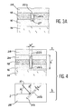
- An exemplary embodiment of a separating blade in integrated optics as described in document FR-A-2 613 826 filed in the name of the applicant is shown in Figure 1. Part a of Figure 1 is a sectional view of the separating blade and part b a top view.
- the light guide in which the separating plate is formed consists (part a) of a silicon substrate 2, surmounted by a buffer or lower layer 3 made of undoped silica and then by a guide layer 4 made of Si3N4 of index of refraction higher than that of the lower layer 3.
- the separating blade 6 consists of a trench formed in the upper layer 5, the depth of which is, in this representation, equal to the thickness of the upper layer 5.
- two different guide structures can be defined: a structure (1) Si / SiO2 / Si3N4 / SiO2 with effective index N1eff and a structure (2) Si / SiO2 / Si3N4 / air with effective index N2eff.
- the effective index of a structure depends on the refractive index of the layers constituting it and their thickness.
- I represents the incident light beam
- R represents the reflected light beam
- T represents the light beam transmitted by the blade 6
- N represents the normal to the blade 6.
- the laser diodes use guiding structures having very high refractive index variations between the core and the surrounding medium while the optical fibers have low refractive index variations (of the order of 4.10 ⁇ 3 at 10 ⁇ 2).
- the confinement of light is very different; 1 micrometer or less (in the direction of the junction) for the laser diode and 5 to 9 micrometers for the optical fibers.
- the two guide structures are stacked.
- the subject of the invention is precisely an integrated optical component as well as its manufacturing method making it possible to remedy the various drawbacks given above.
- this optical component is protected against the environment while ensuring high effective index variations.
- this component when this component is a network, it can be used for efficient co-directive coupling of two stacked optical guides having very different guided mode profiles.
- the component of the invention can be produced from a greater number of materials than those of the prior art and its manufacture is much less critical.
- the invention relates to an integrated optical component, protected against the environment, comprising at least one closed cavity isolated from the environment and formed in at least one layer of a light guide, this cavity being filled with a material having a different refractive index or which can be made different from the refractive index of said layer.
- the filling material enclosed in the cavity allows a local modification of the effective index of the light guide higher than that obtained in the components of the prior art.
- this local modification of the effective index is fixed only by the filling material of the cavity and therefore does not undergo polluting disturbances due to the environment.
- the filling material of the cavity is in particular an organic fluid or polymer.
- the fluid used can be a gas or a liquid and its refractive index can be lower or higher than that of the layer containing it.
- the difference in index created by the cavity is negative, light only exists in an evanescent form in components of the network or coupler type. This ensures good reproducibility of the desired performances as a result of a reduction in sensitivity to the thickness of the cavity, for example.
- the transition from a monomode structure to a multimode structure may pose problems of intermodal parasitic coupling, it is possible to use a material with a higher refractive index than that of the layer containing the filling material.
- a neutral or inert gas such as for example argon, neon, helium, nitrogen, or use air or vacuum.
- gases all have a refractive index lower than that of silica, equal to or close to 1.
- the gases also have the advantage of not causing long-term chemical reactions with the materials of the integrated structure and therefore of not not modify the physical properties sought for the structure.
- air is used as the filling material. Its refractive index equal to 1 makes it possible to associate it with a large number of materials and to ensure a large difference in effective index.
- gases or vapors having particular absorption lines which can for example be optically saturated, (the excitation of the energy levels corresponding to these absorption lines), such as helium, neon, sodium or rhubidium vapors.
- the integrated optical component of the invention allows the use of liquid, which was not possible in the components of the prior art. This increases the number of possibilities of components to be produced.
- a liquid allows in particular the production of new components of the optical valve, modulator or deflector type. And this is particularly the case when using electrically controllable liquids such as electrolytes or liquid crystals such as nematic or smectic C liquid crystals.
- this liquid material having a refractive index (1.65) higher than that of silica, or organic polymers (PMMA, polyimide for example) d refractive index (ranging from 1.45 to 1.7) also higher than that of silica.
- the CS2 has the advantage of having a refractive index which can be modified optically.
- Its index can be modified by the action of a light beam which can be a guided beam or an additional external beam sent onto the structure through the upper layers (which must then be transparent at wavelength excitation) or through the lower layers (which must then be transparent at the excitation wavelength).
- a light beam which can be a guided beam or an additional external beam sent onto the structure through the upper layers (which must then be transparent at wavelength excitation) or through the lower layers (which must then be transparent at the excitation wavelength).
- the material can have, when it is not controlled, the same refractive index as the layer or layers which contain it.
- the optical component of the invention can be a mirror.
- the cavity advantageously extends from the upper layer to the lower layer of the light guide.
- the optical component of the invention can also be a separating plate or a focusing lens.
- the dimensions and shape of the cavity define the optical properties of the component.
- the cavity is housed in at least one of the layers of the guide structure.
- the optical component can also be a microguide intended for the lateral confinement of light.
- the optical component is a diffraction grating
- the latter comprises several cavities preferably arranged parallel to each other and each filled with a material of different index; these cavities constitute the lines of the network and are formed in any one of the layers of the guide structure.
- the latter type of component can advantageously be used to couple two guides of superimposed light, with a completely satisfactory energy transfer efficiency.
- the coupling force of a network is proportional to the difference in refractive index between the fluid material in particular contained in the cavities and the material in which these cavities are formed.
- the greater this difference in index the lower the number of lines can be.
- a diffraction grating with a high coupling coefficient in accordance with the invention allows the coupling of two superimposed light guides with very different guided mode profiles, a first guide consisting of a first upper layer and a first lower layer, arranged on one side and on the other side of a first guide layer with a refractive index greater than that of the first upper and lower layers and a second guide consisting of a second upper layer and a second lower layer arranged on either side of a second layer refractive index guide greater than that of the second lower and upper layers, the first upper layer and the second lower layer constituting a single and so-called coupling layer and the network being housed in the coupling layer.
- a diffraction grating according to the invention also allows the coupling of two guides with very different guided mode profiles comprising a first, a second, a third and a fourth stacked layers, the second and the third layers constituting the guide layers respectively of the first and second guides and having refractive indices higher than those of the first and fourth layers, the refractive index of the second layer being also different from that of the third layer, this third layer comprising cavities filled with a material having a different refractive index or which can be made different from that of the third layer.
- the difference in typical refractive index between the guide layer and the adjacent layers is from 5.10 ⁇ 3 to 2.10 ⁇ 2 and for a structure with high index jump, this typical index deviation is from 10 ⁇ 1 to 5.10 ⁇ 1.
- a guide with a large variation in refractive index is for example made up of lower and upper layers of undoped silica of index 1.45 or doped with phosphorus and / or boron, of index 1.46 and a layer guide in silicon nitride of index 2.01 or in silicon oxynitride (SiO x N y with 0 ⁇ x ⁇ 2 and 0 ⁇ y ⁇ 4/3) of index 1.45 to 2, in alumina index 1.65 or in organic materials such as PMMA (polymethyl methacrylate) and polyimides whose index varies from 1.45 to 1.7.
- a light guide with low refractive index variation is in particular made up of lower and upper layers of undoped silica or doped with fluorine and / or boron and of a silica guide layer doped with germanium, titanium, nitrogen or phosphorus.
- Doping of silica with boron or fluorine decreases its refractive index while doping with germanium, phosphorus, nitrogen or titanium increases the refractive index of silica.
- the networks can work in reflective mode, which has the advantage of making them insensitive to technological errors (no networks, width of the cavities, effective indices of the guided modes).
- the mirrors and separating blades of the invention advantageously work in the vicinity of the limit angle of total reflection Al.
- the invention also relates to a method of manufacturing an optical component as defined above.
- the second layer can be deposited by the low pressure CVD technique (LPCVD) or by the plasma assisted CVD technique (PECVD).
- LPCVD low pressure CVD
- PECVD plasma assisted CVD
- the volume and shape of the air bubble depend on the aspect ratio and the properties of the first layer.
- this air bubble it is possible to modify the shape and the volume of this air bubble by carrying out surface treatments of the deposited layers.
- This creep is possible in particular with layers of silica advantageously doped with boron, phosphorus or both so as to lower the temperature of the treatment relative to the creep temperature of the undoped silica.
- This second mode of implementation is of much more general application than the first mode since it allows, unlike the previous mode, the creation of an air bubble whose aspect ratio is less than 0.5 and for example ranging from 0.1 to 0.3.
- this air bubble can be replaced by a liquid or another gas, provided that the latter has a different refractive index or which can be made different from that of the first and second layers, by injection after the deposition of the second layer.
- the injected liquid can be a liquid monomer which can be polymerized by heating or irradiation such as methyl methacrylate which is then polymerized.
- FIGs 2 and 3A there is shown schematically the manufacture of a separating blade according to the invention.
- a monocrystalline silicon substrate 14 on which a layer of silicon oxide 16 is unintentionally doped from 8 to 12 micrometers, for example by high pressure thermal oxidation of the substrate under oxygen atmosphere between 800 and 1200 ° C.
- the refractive index of this oxide layer 16 is approximately 1.45.
- the guide layer 18 is deposited in silicon oxide doped with phosphorus, germanium, nitrogen or titanium, having a thickness of 3.2 to 10 micrometers. Phosphorus doping is provided by 1021 to 1022 atoms / cm3. The refractive index of this layer 18 is close to 1.46.
- a mask 19 of photosensitive resin is formed (part a, FIG. 2) comprising an opening 21 fixing the location of the separating blade as well as its dimensions.
- an anisotropic etching of the layer 18 is then carried out, thus forming a trench 22 in the zone of the layer 18 located opposite the opening 21 of the mask.
- This etching is for example a reactive ion etching (GIR) using CHF3 or CF4 as an attack agent.
- the h / w ratio is at least equal to 0.5.
- a separating plate must have a reflection coefficient of between 30 and 70%. Roughly, it is enough that h is of the order of the magnitude of half of the spatial extension (or spatial width of the guided mode).
- h can be equal to 3.4 micrometers and w equal to 2.5 micrometers, and in FIG. 3A, h can be equal to 5 micrometers for the same value of w.
- a layer 24 of unintentionally doped silicon oxide 1 to 6 micrometers thick or possibly containing a dopant decreasing the refractive index of the oxide is deposited like boron or fluorine with concentrations of 1021 to 1022 atoms / cm3.
- This layer is deposited by the plasma vapor deposition technique assisted by a plasma (PECVD) at temperatures of 300 to 500 ° C by thermal decomposition of silane and oxygen or by the low pressure vapor deposition technique (130 Pa) with these same gases (LPCVD).
- PECVD plasma vapor deposition technique assisted by a plasma
- LPCVD low pressure vapor deposition technique
- the deposition by PECVD or LPCVD of a layer of silica necessarily leads, for h / w ⁇ 0.5, to the formation of a cavity 26 or 26a containing air 27 housed in the trench respectively 22, 22a.
- the presence of this air bubble causes a significant local modification of the effective index of the guided mode.
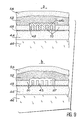
- the reflection coefficient R ( Figure 1b) of the separating plate thus formed goes from 0 to 95% when h varies from 0 to 5 micrometers, w being fixed at 2.5 micrometers.
- h 3.4 micrometers the coefficients of transmission and reflection of the plate are close to 50% and the limit angle of reflection Al is close to 45 °.
- the trench 22c over all or part of the upper layer 24 of the guide.
- the etching of layer 24 is followed by the deposition of a layer 28 of undoped SiO2, from 1 to 10 micrometers thick by PECVD or LPCVD under the same conditions as described in FIG. 2 for layer 24
- a cavity 26e filled with air the shape of which is fixed by the height / width ratio of the trench 22c.
- the guide layer, referenced 17, is made of silicon nitride deposited by LPCVD and has a thickness of 100 to 400nm.
- FIG. 4 there is shown schematically an integrated mirror conforming to the invention. As before, this mirror is formed in a wave guide made of Si / SiO2 / SiO2 doped + / SiO2. The deposition techniques and the thicknesses of these layers are identical to those described with reference to FIG. 2.
- anisotropic etching of the stack of layers 16, 18 and 24 is performed using an appropriate mask (see FIG. 2a). ′ The depth of the trench 22b formed and w ′ its width. This etching is carried out over the entire thickness of the layers 24 and 18 and on all or only part of the layer 16; the attacking agents are for example CHF4 or CF4.
- an undoped silicon oxide layer 28 of 1 to 10 micrometers is deposited with PECVD or LPCVD under the same conditions as described in FIG. 2 for layer 24.
- a bubble is thus formed 26b air whose shape is fixed by the ratio h ′ / w ′ of the trench 22b.
- the width w ′ of the trench 22b must be greater than a minimum value wo in order to avoid any recoupling of the guided mode in the guide structure.
- I and R represent the incident and reflected beams respectively and N represents the normal to the mirror defined by the trench 22b.
- the angle A between the normal and the incident beam must be greater than the total reflection angle Al defined in equation (2):
- Al ArcsinN2 / N1eff (2) where N1eff is the effective index of the guided mode and N2 represents the index of the air bubble, i.e. 1.
- N1eff is of the order of 1.47 and Al of the order of 43 °. So, A must be greater than 43 °.
- the above formula (2) is especially applicable to the mirror; it corresponds to the case where the guided mode no longer exists in the cavity containing the fluid. However, it can be used in place of formula (1) for the separating plates, depending on the value of the reflection coefficient sought.
- the evanescent wave associated with the total reflection on the mirror 22b has a depth of penetration given by the function:
- This function has a value equal to 1 / e when
- width w ′ is much greater than 450 nm and for example equal to 3 or 4 micrometers, practically no light energy can pass through the air bubble 26b.
- the mirror thus formed is very efficient.
- the expression: is much greater than 1, with wm the minimum value of w ′.
- the depth h ′ is not critical; it is enough that it is greater than a minimum value ho roughly equal to the spatial width of the guided mode.
- the spatial width of the guided mode represents the width at half-height of the profile of the light intensity of the wave which propagates in the guide.
- the waveguide is identical to that described with reference to FIGS. 2 and 3A.
- the pitch of the network p determines the operating angle A, shown in part b of FIG. 5, which is the angle formed by the incident beam with the lines 30 of the network.
- the deposition of the SiO2 layer 24 by LPCVD or PECVD on the guide layer 18 leads to the formation of bubbles and therefore to cavities 26c filled with air 27, housed in each of the trenches 30.
- the depth of the trenches h and the index of the material which fills these trenches, here the air, determine the coupling coefficient K between the network and the incident beam and therefore the coupling width Lc ⁇ / 2K of the guided mode with the network.
- the creation of air bubbles 26c of index 1 increases the value of K and therefore decreases the coupling length Lc. This makes the network less sensitive to wavelengths.
- the network Since it is difficult to control the value of the coupling coefficient K which strongly depends on h and on the shape of the bubbles 26c, the network is systematically made to work in reflection. This also makes it possible to make the network less sensitive to technological errors, in particular on the value of the pitch, the width of the trenches or on the effective indices of the guided modes.
- the air can be replaced by nematic or smectic liquid crystals C, the refractive index of which can be controlled electrically, by injection into the cavities of these liquid crystals.
- the air initially present in the cavity 31 formed in the trench 22a is replaced by a smectic liquid crystal C 32 and electrodes 34, 36 of conductive metal such as aluminum are deposited on the light guide.
- these electrodes 34 and 36 are arranged on the layer 24, the electrode 34 being placed opposite the liquid crystal 32 or, as shown in FIG. B, the electrode 34 is arranged on the layer 24 facing the liquid crystal 32 and the electrode 36 on the rear face of the guide, that is to say on the substrate 14.
- the electrode 34 facing the liquid crystal is brought to a potential + and the electrode 36 to ground.
- the dotted lines 33 represented in FIG. 6 (a) symbolize the lines of the electric field applied to the optical component.
- FIG 7 there is shown another method of manufacturing the components according to the invention and in particular the manufacture of a separating or semi-reflecting plate.
- a layer 38 of a material 38 which can be selectively etched relative to the layer 18 and to the layer is deposited over the entire structure (part a).
- upper layer 24 of the optical guide In the case of layers 18 and 24 of silica, a metal layer and in particular a layer of aluminum or chromium can be used.
- This layer 38 can be deposited by any known deposition technique and in particular by cathode sputtering or by electrolytic deposition for a metal layer.
- This layer has a thickness greater than that of the trench 22.
- the layer 38 has for example a thickness of 10 micrometers.
- This layer is then selectively etched so as to keep metal at least opposite the trench 22, that is to say in and above the trench (metal which can also be kept on either side of the trench) .
- This engraving is carried out using a photolithography mask, not shown.
- the metal stud obtained is referenced 38a (part b).
- the deposition of the silica layer 24 is then carried out.
- This deposition can be carried out by all known deposition techniques and in particular by CVD using silane and oxygen as deposition gas.
- a selective attack of the metal pad 38a leading to its complete elimination can be done by a chemical attack in solution from a hole made for example in layer 24 and connected to the metal.
- a phosphoric acid solution is used and for chromium, a cerium salt solution.
- This method allows you to use all deposition techniques for constituting layer 24. In addition, it applies to all values of h / w greater than 0.1 while the method described in FIG. 2 can only be used for ratios of h / w greater at 0.5.
- the guide structure with a large variation in refractive index denoted A, consists for example of a lower layer 44 of refractive index n1 deposited on a substrate 46, of a guide layer 48 of refractive index n2 and an upper layer 50 of refractive index n3, with the layer 48 interposed between the layers 44 and 50 and n2 greater than n1 and n3.
- the guide structure with low index variation denoted B, consists for example of layer 50, a guide layer 52 of refractive index n4 and an upper layer 54 of refractive index n5, with the layer 52 sandwiched between layers 50 and 54 and n4 greater than n3 and n5.
- n4 must be greater than n1 and n2 must be greater than n4 (the order of superposition of structures A and B can of course be reversed).
- the layers 44, 50 and 54 can be made of unintentionally doped silica or doped with fluorine or boron; layer 48 can be made of silicon nitride, silicon oxynitride or alumina and layer 52 of silica doped with phosphorus, germanium, nitrogen or titanium.
- the layers 48, 50, 52 and 54 can be deposited by LPCVD or PECVD and the layer 44 formed by thermal oxidation of the substrate, so as to have good optical qualities.
- the thickness of the layer 48 is less than the maximum value to be single mode, of the order of 0.05 to 0.4 micrometer depending on the wavelengths used for a silicon nitride layer, and that the thickness of the layer 52 is also less than a maximum value for being single-mode, of the order of 1 to 8 micrometers depending on the wavelengths used and the index differences chosen between the different layers.
- the thickness e1 of the layer 44 must ensure the isolation of the two propagation nodes of the guides A and B of the substrate 46. Also, this thickness must be greater than the penetration depth of the evanescent wave of the guided mode the least confined which propagates in layer 52. Typically, e1 is greater than 12-15 micrometers.
- the thickness of the layer 50 conditions the coupling force of the network. It can be zero (figure 11).
- the coupling between the two guided modes decreases with the thickness of the layer 50. Beyond 3 micrometers for layers of silica and for a layer 48 of silicon nitride with a thickness of the order of 50 nm, the coupling no longer exists.
- the thickness of layer 54 is not critical.
- the layers 44, 48, 50, 52 and 54 respectively have a thickness of 8 to 15 micrometers, from 50 to 200 nm, from 0.3 to 2 micrometers, from 1 to 8 micrometers and from 2 to 10 micrometers.
- the pitch of the network and the angle of incidence on this network are chosen to allow the network 40 to work in reflection from so as to prevent the coupled light energy from the structure with high index variation towards the structure with small index variation from being able to return to the structure with high index variation.
- the coupling network 40 can be obtained by etching the layer 50 just before depositing the guide layer 52, so as to form trenches 42 parallel to one another whose height / width ratio is at least equal to 0.5 then by depositing the layer 52 by LPCVD or PECVD, as described previously with reference to FIG. 2.
- cavities 41 filled with air bubbles 27 formed during the deposition of the layer 52 and housed in the trenches 42 ensure the coupling of the two guide structures.
- these cavities 41 are 10 to 30 in number and the pitch of the network is 0.3 to 3 micrometers.
- FIG. 9 shows another embodiment of the diffraction grating ensuring the coupling of the two guide structures.
- the etched layer 50 is carried out (part a) the deposition of a metallic layer which can be etched selectively with respect to the substrate 46 and to the layers 44, 48, 50, 52 and possibly 54 when the metal is removed after the deposition of the layer 54, then this layer is etched so as to keep metal 38b only next to the trenches 43 made in layer 50.
- the etching of this metal layer is followed by the deposition of layers 52 and 54, as described above with reference to FIGS. 2 and 7. (Of course, this layer 54 can also be deposited after the total elimination of the metal).
- metal 38b is removed using orthophosphoric acid for an aluminum layer and guide structures in Si / SiO2 / Si3N4 / SiO2 / SiO2 doped + / SiO2, via at least one through hole. for example the layers overhanging the metal 38b.
- the space initially occupied by the metal 38b and in particular the trenches 43 is then filled with air 27 (part b of FIG. 9).
- the coupling network can also be produced as shown in FIG. 10.
- the metal layer 38 is deposited directly on the entire guide layer 48 (part a of FIG. 10).
- a substantially anisotropic etching of the layer 38 is then carried out so as to form metal studs 38c parallel to each other and equidistant.
- this anisotropic etching is carried out dry with a chlorinated gas or wet with othophosphoric acid as attacking agent.
- the layers 50, 52, 54 (part b) are deposited as described above.
- the etched metal studs 38c are eliminated by the wet method, giving rise to cavities 45 filled with air.
- the layers 52 and 54 can in this case be arranged before or after elimination of the metal studs. To be eliminated, these metal studs are connected together in layer 50, outside the useful zone of the component, at least one hole made in layer 50 allowing access to the metal 38.
- This method can pose some difficulties for very small network pitches, less than 1 micrometer with regard to the elimination of the metal studs 38c, unlike the method described in FIG. 9.
- the layer 50 may have a zero thickness, as shown in Figure 11.
- the layer 52 is directly deposited on the metal pads 38c.
- the studs are eliminated as above.
- FIGS. 5 and 8 to 11 networks with constant steps have been shown which therefore work with collimated incident beams.
- networks similar to those shown associated with collimation optics of the integrated mirror or lens type according to the invention or alternatively to use a network whose features are elliptical or parabolic, or else use a variable-pitch network providing both the coupling and imaging function. This allows, in some cases, to decrease the number of components of a complete optical circuit.
- guide structures with small index variation are insensitive to the polarization of the incident beam unlike guide structures with high index variation. Also, it is very difficult to separate spatially or even, more simply, to select one of the transverse electric polarizations TE or transverse magnetic TM of the guide mode in a structure with low index variation.
- the air contained in the cavities of the networks can be replaced by another gas or a liquid in particular, which one can electrically and / or optically modify the refractive index.
- the components of the invention can be formed in other materials than those mentioned above and in particular in lithium niobate or tantalate.
- a microguide according to the invention produced in a Si / SiO2 / Si3N4 / SiO2 guide structure.
- This microguide comprises in its upper layer 50 made of SiO2 two cavities 26f, 26g filled with air.
- the difference in index between the air and the silica of the layer 50 ensures good lateral confinement of the light.
- These cavities are obtained by making two trenches 22d and 22e parallel in the layer 50 then by depositing by LPCVD or PECVD a layer 28 of non-doped SiO2.
- the trenches can be formed in all or part of the layer 50 or 44 but not in the guide layer 48.
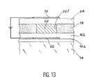
- FIG. 13 another embodiment of an active component according to the invention is shown, of the separating blade type, the reflection coefficient of which can be controlled electrically.
- This component is produced in a guide structure Si / SiO2 / SiO2 doped + / SiO2.
- This component comprises in its guide layer 18 a trench 22f filled with an organic polymer 56 whose refractive index can be modified by applying a voltage to it via electrodes 58 and 60 made of aluminum parallel to the layers of the guiding structure and in particular to polymer 56.
- the upper electrode 58 is arranged on the upper layer 24 of the guide opposite the polymer 56.
- the lower electrode 60 is arranged in the layer 16, constituted in this case for practical reasons, of two layers 16a and 16b superimposed on same composition.
Landscapes
- Physics & Mathematics (AREA)
- Engineering & Computer Science (AREA)
- Microelectronics & Electronic Packaging (AREA)
- General Physics & Mathematics (AREA)
- Optics & Photonics (AREA)
- Optical Integrated Circuits (AREA)
Applications Claiming Priority (2)
| Application Number | Priority Date | Filing Date | Title |
|---|---|---|---|
| FR9004255 | 1990-04-03 | ||
| FR9004255A FR2660440B1 (fr) | 1990-04-03 | 1990-04-03 | Composant optique integre protege contre l'environnement et son procede de fabrication. |
Publications (2)
| Publication Number | Publication Date |
|---|---|
| EP0451047A1 true EP0451047A1 (de) | 1991-10-09 |
| EP0451047B1 EP0451047B1 (de) | 1997-10-29 |
Family
ID=9395403
Family Applications (1)
| Application Number | Title | Priority Date | Filing Date |
|---|---|---|---|
| EP91400893A Expired - Lifetime EP0451047B1 (de) | 1990-04-03 | 1991-04-02 | Vor Umwelteinflüssen geschützte integrierte optische Komponente und Verfahren zu ihrer Herstellung |
Country Status (6)
| Country | Link |
|---|---|
| US (1) | US5210801A (de) |
| EP (1) | EP0451047B1 (de) |
| JP (1) | JPH04230708A (de) |
| CA (1) | CA2039526A1 (de) |
| DE (1) | DE69128045T2 (de) |
| FR (1) | FR2660440B1 (de) |
Cited By (7)
| Publication number | Priority date | Publication date | Assignee | Title |
|---|---|---|---|---|
| EP0557713A1 (de) * | 1992-02-24 | 1993-09-01 | Corning Incorporated | Planarer optischer Wellenleiter mit planaren optischen Elementen |
| EP0589268A1 (de) * | 1992-09-17 | 1994-03-30 | Robert Bosch Gmbh | Integriert optische Schaltung mit einer Bragg-Struktur |
| EP0701150A1 (de) * | 1994-09-09 | 1996-03-13 | AT&T Corp. | Verfahren zum Herstellen von Braggreflektoren für Wellenleiter und damit erhaltene Produkte |
| FR2748328A1 (fr) * | 1996-05-02 | 1997-11-07 | Loisel Bertrand | Guide optique a reseau de bragg et a coeur en silice |
| EP0887668A1 (de) * | 1997-06-26 | 1998-12-30 | Alcatel Alsthom Compagnie Generale D'electricite | Bragg-Reflektor in einem Halbleiter und Herstellungsverfahren |
| WO1999064905A1 (fr) * | 1998-06-11 | 1999-12-16 | Centre National De La Recherche Scientifique - Cnrs | Dispositif de diffraction de lumiere enfoui dans un materiau |
| WO2006007875A1 (en) * | 2004-07-22 | 2006-01-26 | Pirelli & C. S.P.A. | Optical device including a buried grating with air filled voids and method for realising it |
Families Citing this family (66)
| Publication number | Priority date | Publication date | Assignee | Title |
|---|---|---|---|---|
| US5289308A (en) * | 1991-12-20 | 1994-02-22 | Akzo N.V. | Method of making a frequency doubling structure in an optically non-linear medium |
| US5282078A (en) * | 1991-12-20 | 1994-01-25 | Akzo Nv | Method of making a frequency doubling structure in an optically non-linear medium, and a frequency doubling device |
| DE4200396C1 (de) * | 1992-01-10 | 1993-02-04 | Imm Institut Fuer Mikrotechnik Gmbh, 6500 Mainz, De | |
| DE4200397C1 (de) * | 1992-01-10 | 1993-03-04 | Imm Institut Fuer Mikrotechnik Gmbh, 6500 Mainz, De | |
| US5356722A (en) * | 1992-06-10 | 1994-10-18 | Applied Materials, Inc. | Method for depositing ozone/TEOS silicon oxide films of reduced surface sensitivity |
| SG125045A1 (en) * | 1992-06-24 | 2006-09-29 | British Telecomm | Optical device including refractive index modulation |
| US6229945B1 (en) * | 1992-06-24 | 2001-05-08 | British Telecommunications Public Limited Company | Photo induced grating in B2O3 containing glass |
| US5917625A (en) * | 1993-09-09 | 1999-06-29 | Kabushiki Kaisha Toshiba | High resolution optical multiplexing and demultiplexing device in optical communication system |
| FR2716012B1 (fr) * | 1994-02-09 | 1996-04-12 | Corning Inc | Procédé et dispositif d'assemblage d'extrémités de fibres optiques disposées en nappe. |
| US5503902A (en) * | 1994-03-02 | 1996-04-02 | Applied Physics Research, L.P. | Light control material |
| SE503740C2 (sv) * | 1994-04-22 | 1996-08-19 | Ericsson Telefon Ab L M | Optisk fiber innefattande en reflektor samt sätt att framställa en reflektor i en optisk fiber |
| US5440421A (en) * | 1994-05-10 | 1995-08-08 | Massachusetts Institute Of Technology | Three-dimensional periodic dielectric structures having photonic bandgaps |
| US5600483A (en) * | 1994-05-10 | 1997-02-04 | Massachusetts Institute Of Technology | Three-dimensional periodic dielectric structures having photonic bandgaps |
| JPH10506756A (ja) * | 1994-10-05 | 1998-06-30 | マサチューセッツ インスティトゥート オブ テクノロジー | 一次元周期誘導体導波路を使用する共振微小空洞 |
| US5784400A (en) * | 1995-02-28 | 1998-07-21 | Massachusetts Institute Of Technology | Resonant cavities employing two dimensionally periodic dielectric materials |
| US5732168A (en) * | 1995-10-31 | 1998-03-24 | Hewlett Packard Company | Thermal optical switches for light |
| JP3929495B2 (ja) * | 1996-01-18 | 2007-06-13 | ブリティッシュ・テレコミュニケーションズ・パブリック・リミテッド・カンパニー | 光感応性屈折率クラッドを備えた光導波路 |
| US5699462A (en) * | 1996-06-14 | 1997-12-16 | Hewlett-Packard Company | Total internal reflection optical switches employing thermal activation |
| US6149974A (en) * | 1997-05-05 | 2000-11-21 | Applied Materials, Inc. | Method for elimination of TEOS/ozone silicon oxide surface sensitivity |
| JPH11194237A (ja) * | 1997-12-26 | 1999-07-21 | Nec Corp | 光導波路とその製造方法及び光導波路と受光素子の結合構造 |
| JPH11237514A (ja) * | 1998-02-20 | 1999-08-31 | Shin Etsu Chem Co Ltd | グレーティング用光ファイバ、グレーティング用光ファイバ母材およびその光ファイバ母材の製造方法 |
| US6396988B1 (en) * | 1999-08-13 | 2002-05-28 | Nec Corporation | Optical waveguide device and method of forming the same |
| US6408125B1 (en) | 1999-11-10 | 2002-06-18 | Corning Incorporated | Germanium silicon oxynitride high index films for planar waveguides |
| EP1116967A1 (de) * | 2000-01-13 | 2001-07-18 | Contraves Space AG | Lichtwellenleiterkoppler |
| CA2423283A1 (en) * | 2000-09-29 | 2003-03-24 | Schott Glas | Optical substrate and method and device for producing optical substrates |
| WO2002048765A1 (en) * | 2000-12-14 | 2002-06-20 | Bookham Technology Plc | Integrated optical devices |
| US6532319B2 (en) * | 2000-12-18 | 2003-03-11 | Agilent Technologies, Inc. | Ceramic substrate for photonic switching system |
| US6787868B1 (en) | 2001-09-25 | 2004-09-07 | Lightwave Microsystems Corporation | Microlenses for integrated optical devices |
| US6798939B2 (en) * | 2002-03-14 | 2004-09-28 | Agilent Technologies, Inc. | Bubble stability in an optical switch |
| EP1506440A4 (de) * | 2002-05-17 | 2005-08-10 | Nanoventions Inc | Planarer optischer wellenleiter |
| US6709969B1 (en) * | 2002-12-19 | 2004-03-23 | Mark E. Murray | Method for fabricating a gas insulated gate field effect transistor |
| US7349612B2 (en) * | 2003-01-28 | 2008-03-25 | Nippon Sheet Glass Company, Limited | Optical element, optical circuit provided with the optical element, and method for producing the optical element |
| US7206480B2 (en) * | 2003-08-01 | 2007-04-17 | Bae Systems Information And Electronic Systems Integration Inc. | Method of forming interlayer connections in integrated optical circuits, and devices formed using same |
| ITRM20040445A1 (it) * | 2004-09-17 | 2004-12-17 | St Microelectronics Srl | Processo per scavare trincee in un dispositivo ottico integrato. |
| JP2006337748A (ja) * | 2005-06-02 | 2006-12-14 | Fuji Xerox Co Ltd | 光導波路及びその製造方法 |
| US20070154156A1 (en) * | 2005-12-30 | 2007-07-05 | Gary Brist | Imprinted waveguide printed circuit board structure |
| US7561773B2 (en) * | 2006-06-19 | 2009-07-14 | Fuji Xerox Co., Ltd. | Optical waveguide, method of manufacturing the same and optical communication module |
| JP2008020722A (ja) * | 2006-07-13 | 2008-01-31 | Fuji Xerox Co Ltd | 光導波路及びその製造方法 |
| JP2009145867A (ja) * | 2007-11-22 | 2009-07-02 | Sumitomo Bakelite Co Ltd | 光導波路、光導波路モジュールおよび光素子実装基板 |
| WO2010023976A1 (ja) * | 2008-08-26 | 2010-03-04 | 住友ベークライト株式会社 | 光導波路、光導波路モジュールおよび光素子実装基板 |
| US11726332B2 (en) | 2009-04-27 | 2023-08-15 | Digilens Inc. | Diffractive projection apparatus |
| JP2010049280A (ja) * | 2009-11-25 | 2010-03-04 | Seiko Epson Corp | 偏光素子の製造方法 |
| WO2016020630A2 (en) | 2014-08-08 | 2016-02-11 | Milan Momcilo Popovich | Waveguide laser illuminator incorporating a despeckler |
| EP2842003B1 (de) | 2012-04-25 | 2019-02-27 | Rockwell Collins, Inc. | Holographisches weitwinkeldisplay |
| US9933684B2 (en) | 2012-11-16 | 2018-04-03 | Rockwell Collins, Inc. | Transparent waveguide display providing upper and lower fields of view having a specific light output aperture configuration |
| WO2016042283A1 (en) | 2014-09-19 | 2016-03-24 | Milan Momcilo Popovich | Method and apparatus for generating input images for holographic waveguide displays |
| US10437064B2 (en) | 2015-01-12 | 2019-10-08 | Digilens Inc. | Environmentally isolated waveguide display |
| US9632226B2 (en) | 2015-02-12 | 2017-04-25 | Digilens Inc. | Waveguide grating device |
| WO2017060665A1 (en) | 2015-10-05 | 2017-04-13 | Milan Momcilo Popovich | Waveguide display |
| US10416380B1 (en) * | 2016-06-23 | 2019-09-17 | Acacia Communications, Inc. | Suspended photonic waveguides with top side sealing |
| EP3548939A4 (de) | 2016-12-02 | 2020-11-25 | DigiLens Inc. | Wellenleitervorrichtung mit gleichmässiger ausgabebeleuchtung |
| US10545346B2 (en) | 2017-01-05 | 2020-01-28 | Digilens Inc. | Wearable heads up displays |
| JP7404243B2 (ja) | 2018-01-08 | 2023-12-25 | ディジレンズ インコーポレイテッド | 導波管セル内のホログラフィック格子の高スループット記録のためのシステムおよび方法 |
| CN114721242B (zh) | 2018-01-08 | 2025-08-15 | 迪吉伦斯公司 | 用于制造光学波导的方法 |
| JP7456929B2 (ja) | 2018-01-08 | 2024-03-27 | ディジレンズ インコーポレイテッド | 導波管セルを製造するためのシステムおよび方法 |
| WO2020149956A1 (en) | 2019-01-14 | 2020-07-23 | Digilens Inc. | Holographic waveguide display with light control layer |
| US20200247017A1 (en) | 2019-02-05 | 2020-08-06 | Digilens Inc. | Methods for Compensating for Optical Surface Nonuniformity |
| US20220283377A1 (en) | 2019-02-15 | 2022-09-08 | Digilens Inc. | Wide Angle Waveguide Display |
| EP3924759B1 (de) | 2019-02-15 | 2025-07-30 | Digilens Inc. | Verfahren und vorrichtungen zur herstellung einer holografischen wellenleiteranzeige mit integrierten gittern |
| EP3980825A4 (de) | 2019-06-07 | 2023-05-03 | Digilens Inc. | Wellenleiter mit durchlässigen und reflektierenden gittern sowie zugehörige herstellungsverfahren |
| JP2022546413A (ja) | 2019-08-29 | 2022-11-04 | ディジレンズ インコーポレイテッド | 真空回折格子および製造方法 |
| WO2022056264A1 (en) | 2020-09-11 | 2022-03-17 | Shanghai Yanfeng Jinqiao Automotive Trim Systems Co. Ltd. | Vehicle interior component |
| WO2022150841A1 (en) | 2021-01-07 | 2022-07-14 | Digilens Inc. | Grating structures for color waveguides |
| KR20230153459A (ko) | 2021-03-05 | 2023-11-06 | 디지렌즈 인코포레이티드. | 진공 주기적 구조체 및 제조 방법 |
| CN119173882A (zh) * | 2022-05-10 | 2024-12-20 | 三菱电机株式会社 | 可重构波长选择性分束器 |
| US12306442B2 (en) * | 2022-08-02 | 2025-05-20 | Globalfoundries U.S. Inc. | Structure including grating coupler with optofluidic grating channels |
Citations (2)
| Publication number | Priority date | Publication date | Assignee | Title |
|---|---|---|---|---|
| EP0196948A1 (de) * | 1985-03-13 | 1986-10-08 | Commissariat A L'energie Atomique | Umkehrbare Demultiplexeinrichtung von einer Mehrzahl von Lichtsignalen in integrierter Optik |
| EP0286528A1 (de) * | 1987-04-07 | 1988-10-12 | Commissariat A L'energie Atomique | Optisch integrierter Verschiebungssensor |
Family Cites Families (8)
| Publication number | Priority date | Publication date | Assignee | Title |
|---|---|---|---|---|
| DE7706786U1 (de) * | 1977-03-05 | 1977-06-08 | Jenaer Glaswerk Schott & Gen., 6500 Mainz | Lichtleitfaser mit querlicht |
| GB8516108D0 (en) * | 1985-06-26 | 1985-07-31 | Gen Electric Co Plc | Optical switch |
| JPS6294823A (ja) * | 1985-10-22 | 1987-05-01 | Nippon Telegr & Teleph Corp <Ntt> | 導波形光変調器 |
| US4888785A (en) * | 1988-01-19 | 1989-12-19 | Bell Communications Research, Inc. | Miniature integrated optical beam splitter |
| US4932743A (en) * | 1988-04-18 | 1990-06-12 | Ricoh Company, Ltd. | Optical waveguide device |
| US5074629A (en) * | 1988-10-26 | 1991-12-24 | Stanford University | Integrated variable focal length lens and its applications |
| US4961617A (en) * | 1989-07-19 | 1990-10-09 | Ferrydon Shahidi | Fibre optic waveguide illuminating elements |
| US4988157A (en) * | 1990-03-08 | 1991-01-29 | Bell Communications Research, Inc. | Optical switch using bubbles |
-
1990
- 1990-04-03 FR FR9004255A patent/FR2660440B1/fr not_active Expired - Lifetime
-
1991
- 1991-03-22 US US07/673,386 patent/US5210801A/en not_active Expired - Fee Related
- 1991-04-02 EP EP91400893A patent/EP0451047B1/de not_active Expired - Lifetime
- 1991-04-02 DE DE69128045T patent/DE69128045T2/de not_active Expired - Fee Related
- 1991-04-02 CA CA002039526A patent/CA2039526A1/en not_active Abandoned
- 1991-04-03 JP JP3150830A patent/JPH04230708A/ja active Pending
Patent Citations (2)
| Publication number | Priority date | Publication date | Assignee | Title |
|---|---|---|---|---|
| EP0196948A1 (de) * | 1985-03-13 | 1986-10-08 | Commissariat A L'energie Atomique | Umkehrbare Demultiplexeinrichtung von einer Mehrzahl von Lichtsignalen in integrierter Optik |
| EP0286528A1 (de) * | 1987-04-07 | 1988-10-12 | Commissariat A L'energie Atomique | Optisch integrierter Verschiebungssensor |
Non-Patent Citations (1)
| Title |
|---|
| PATENT ABSTRACTS OF JAPAN, vol. 11, no. 303 (P-622)[2750], 03 octobre 1987; & JP-A-62 094 823 (NTT CORP.) 01-05-1987 * |
Cited By (12)
| Publication number | Priority date | Publication date | Assignee | Title |
|---|---|---|---|---|
| EP0557713A1 (de) * | 1992-02-24 | 1993-09-01 | Corning Incorporated | Planarer optischer Wellenleiter mit planaren optischen Elementen |
| AU661890B2 (en) * | 1992-02-24 | 1995-08-10 | Corning Incorporated | Planar optical waveguides with planar optical elements |
| US5612171A (en) * | 1992-02-24 | 1997-03-18 | Corning Incorporated | Planar optical waveguides with planar optical elements |
| EP0589268A1 (de) * | 1992-09-17 | 1994-03-30 | Robert Bosch Gmbh | Integriert optische Schaltung mit einer Bragg-Struktur |
| EP0701150A1 (de) * | 1994-09-09 | 1996-03-13 | AT&T Corp. | Verfahren zum Herstellen von Braggreflektoren für Wellenleiter und damit erhaltene Produkte |
| FR2748328A1 (fr) * | 1996-05-02 | 1997-11-07 | Loisel Bertrand | Guide optique a reseau de bragg et a coeur en silice |
| EP0887668A1 (de) * | 1997-06-26 | 1998-12-30 | Alcatel Alsthom Compagnie Generale D'electricite | Bragg-Reflektor in einem Halbleiter und Herstellungsverfahren |
| FR2765347A1 (fr) * | 1997-06-26 | 1998-12-31 | Alsthom Cge Alcatel | Reflecteur de bragg en semi-conducteur et procede de fabrication |
| US6023354A (en) * | 1997-06-26 | 2000-02-08 | Alcatel | Semiconductor Bragg reflector and a method of fabricating said reflector |
| WO1999064905A1 (fr) * | 1998-06-11 | 1999-12-16 | Centre National De La Recherche Scientifique - Cnrs | Dispositif de diffraction de lumiere enfoui dans un materiau |
| FR2779835A1 (fr) * | 1998-06-11 | 1999-12-17 | Centre Nat Rech Scient | Dispositif de diffraction de lumiere enfoui dans un materiau |
| WO2006007875A1 (en) * | 2004-07-22 | 2006-01-26 | Pirelli & C. S.P.A. | Optical device including a buried grating with air filled voids and method for realising it |
Also Published As
| Publication number | Publication date |
|---|---|
| FR2660440B1 (fr) | 1992-10-16 |
| DE69128045D1 (de) | 1997-12-04 |
| CA2039526A1 (en) | 1991-10-04 |
| FR2660440A1 (fr) | 1991-10-04 |
| DE69128045T2 (de) | 1998-04-23 |
| US5210801A (en) | 1993-05-11 |
| EP0451047B1 (de) | 1997-10-29 |
| JPH04230708A (ja) | 1992-08-19 |
Similar Documents
| Publication | Publication Date | Title |
|---|---|---|
| EP0451047B1 (de) | Vor Umwelteinflüssen geschützte integrierte optische Komponente und Verfahren zu ihrer Herstellung | |
| EP0196948B1 (de) | Umkehrbare Demultiplexeinrichtung von einer Mehrzahl von Lichtsignalen in integrierter Optik | |
| EP3610309B1 (de) | Photonischer chip mit integrierter kollimationsstruktur | |
| EP0349038B1 (de) | Einen integrierten Lichtleiter umfassendes Halbleitergerät mit wenigstens einem geraden Teil und einem gebogenen Teil | |
| EP0179507B1 (de) | Koppler zwischen Wellenleitern, monolithbar auf einem Halbleitersubstrat integriert | |
| EP0461991B1 (de) | Integriertes optisches Monomode-Raumfilter und Verfahren zu seiner Herstellung | |
| EP0323317B1 (de) | Verfahren zur Herstellung von Mikro-Lichtleitern mit niedrigen optischen Ausbreitungsverlusten durch Aufbringen von Mehrfachschichten | |
| EP3009879B1 (de) | Elektrooptischer phasenmodulator, und modulationsverfahren | |
| EP3009878B1 (de) | Elektrooptischer phasenmodulator | |
| EP3432043A1 (de) | Optische fokalisierungsvorrichtung mit index-pseudogradienten | |
| EP0539298B1 (de) | Integrierter elektro-optischer Modulator und dessen Herstellungsverfahren | |
| EP0050545B1 (de) | Integrierte Fresnelsche Linse und deren Herstellungsverfahren | |
| EP0561672B1 (de) | Integrierter optischer Verstärker und Laser mit einem solchen Verstärker | |
| EP0360759B1 (de) | Druckwandler mit in einem Substrat integriertem optischem Wellenleiter | |
| EP0210690B1 (de) | Teilerstruktur, diese Strukturen verwendendes optisches Schaltelement und diese Schaltelemente verwendende optische Schaltmatrix | |
| EP0783118A1 (de) | Wellenlängendemultiplexer | |
| WO2002077687A2 (fr) | Spectrometre optique integre a haute resolution spectrale et procede de fabrication | |
| EP0916977A1 (de) | Demultiplexer mit quadratischer spektraler antwort | |
| FR3052872A1 (fr) | Reflecteur optique resonant a multiples couches minces de materiaux dielectriques, capteur optique et dispositif d'amplification laser comportant un tel reflecteur | |
| WO1996011417A1 (fr) | Coupleur optique selectif en longueur d'onde | |
| EP3389097A1 (de) | Fotodiode | |
| EP4441559B1 (de) | Optoelektronischer emitter mit phasengesteuerter gruppenantenne mit optischen antennen zur emission von lichtstrahlung nach einem vorgegebenen emissionsprofil und in vorgegebener richtung | |
| EP4034923B1 (de) | Optisches system und verfahren zu dessen herstellung | |
| EP4557537A1 (de) | Integrierte hochleistungslaseremissionsvorrichtung | |
| EP4390483A1 (de) | Optische kopplungsvorrichtung mit holographischer beugungsstruktur |
Legal Events
| Date | Code | Title | Description |
|---|---|---|---|
| PUAI | Public reference made under article 153(3) epc to a published international application that has entered the european phase |
Free format text: ORIGINAL CODE: 0009012 |
|
| AK | Designated contracting states |
Kind code of ref document: A1 Designated state(s): BE DE GB IT NL SE |
|
| 17P | Request for examination filed |
Effective date: 19920311 |
|
| 17Q | First examination report despatched |
Effective date: 19940624 |
|
| GRAG | Despatch of communication of intention to grant |
Free format text: ORIGINAL CODE: EPIDOS AGRA |
|
| GRAH | Despatch of communication of intention to grant a patent |
Free format text: ORIGINAL CODE: EPIDOS IGRA |
|
| GRAH | Despatch of communication of intention to grant a patent |
Free format text: ORIGINAL CODE: EPIDOS IGRA |
|
| GRAA | (expected) grant |
Free format text: ORIGINAL CODE: 0009210 |
|
| AK | Designated contracting states |
Kind code of ref document: B1 Designated state(s): BE DE GB IT NL SE |
|
| REF | Corresponds to: |
Ref document number: 69128045 Country of ref document: DE Date of ref document: 19971204 |
|
| ITF | It: translation for a ep patent filed | ||
| GBT | Gb: translation of ep patent filed (gb section 77(6)(a)/1977) |
Effective date: 19980105 |
|
| PG25 | Lapsed in a contracting state [announced via postgrant information from national office to epo] |
Ref country code: BE Free format text: LAPSE BECAUSE OF NON-PAYMENT OF DUE FEES Effective date: 19980430 |
|
| PLBE | No opposition filed within time limit |
Free format text: ORIGINAL CODE: 0009261 |
|
| STAA | Information on the status of an ep patent application or granted ep patent |
Free format text: STATUS: NO OPPOSITION FILED WITHIN TIME LIMIT |
|
| 26N | No opposition filed | ||
| BERE | Be: lapsed |
Owner name: COMMISSARIAT A L'ENERGIE ATOMIQUE Effective date: 19980430 |
|
| PGFP | Annual fee paid to national office [announced via postgrant information from national office to epo] |
Ref country code: SE Payment date: 19990329 Year of fee payment: 9 Ref country code: GB Payment date: 19990329 Year of fee payment: 9 |
|
| PGFP | Annual fee paid to national office [announced via postgrant information from national office to epo] |
Ref country code: NL Payment date: 19990429 Year of fee payment: 9 |
|
| PGFP | Annual fee paid to national office [announced via postgrant information from national office to epo] |
Ref country code: DE Payment date: 19990503 Year of fee payment: 9 |
|
| PG25 | Lapsed in a contracting state [announced via postgrant information from national office to epo] |
Ref country code: GB Free format text: LAPSE BECAUSE OF NON-PAYMENT OF DUE FEES Effective date: 20000402 |
|
| PG25 | Lapsed in a contracting state [announced via postgrant information from national office to epo] |
Ref country code: SE Free format text: LAPSE BECAUSE OF NON-PAYMENT OF DUE FEES Effective date: 20000403 |
|
| PG25 | Lapsed in a contracting state [announced via postgrant information from national office to epo] |
Ref country code: NL Free format text: LAPSE BECAUSE OF NON-PAYMENT OF DUE FEES Effective date: 20001101 |
|
| GBPC | Gb: european patent ceased through non-payment of renewal fee |
Effective date: 20000402 |
|
| EUG | Se: european patent has lapsed |
Ref document number: 91400893.3 |
|
| NLV4 | Nl: lapsed or anulled due to non-payment of the annual fee |
Effective date: 20001101 |
|
| PG25 | Lapsed in a contracting state [announced via postgrant information from national office to epo] |
Ref country code: DE Free format text: LAPSE BECAUSE OF NON-PAYMENT OF DUE FEES Effective date: 20010201 |
|
| PG25 | Lapsed in a contracting state [announced via postgrant information from national office to epo] |
Ref country code: IT Free format text: LAPSE BECAUSE OF NON-PAYMENT OF DUE FEES Effective date: 20050402 |