EP0197276A2 - Procédé de fabrication de circuits imprimés et produits ainsi obtenus - Google Patents
Procédé de fabrication de circuits imprimés et produits ainsi obtenus Download PDFInfo
- Publication number
- EP0197276A2 EP0197276A2 EP86102413A EP86102413A EP0197276A2 EP 0197276 A2 EP0197276 A2 EP 0197276A2 EP 86102413 A EP86102413 A EP 86102413A EP 86102413 A EP86102413 A EP 86102413A EP 0197276 A2 EP0197276 A2 EP 0197276A2
- Authority
- EP
- European Patent Office
- Prior art keywords
- printed
- tracks
- sheets
- design
- process according
- Prior art date
- Legal status (The legal status is an assumption and is not a legal conclusion. Google has not performed a legal analysis and makes no representation as to the accuracy of the status listed.)
- Withdrawn
Links
Images



Classifications
-
- H—ELECTRICITY
- H05—ELECTRIC TECHNIQUES NOT OTHERWISE PROVIDED FOR
- H05K—PRINTED CIRCUITS; CASINGS OR CONSTRUCTIONAL DETAILS OF ELECTRIC APPARATUS; MANUFACTURE OF ASSEMBLAGES OF ELECTRICAL COMPONENTS
- H05K3/00—Apparatus or processes for manufacturing printed circuits
- H05K3/10—Apparatus or processes for manufacturing printed circuits in which conductive material is applied to the insulating support in such a manner as to form the desired conductive pattern
- H05K3/20—Apparatus or processes for manufacturing printed circuits in which conductive material is applied to the insulating support in such a manner as to form the desired conductive pattern by affixing prefabricated conductor pattern
- H05K3/207—Apparatus or processes for manufacturing printed circuits in which conductive material is applied to the insulating support in such a manner as to form the desired conductive pattern by affixing prefabricated conductor pattern using a prefabricated paste pattern, ink pattern or powder pattern
-
- H—ELECTRICITY
- H05—ELECTRIC TECHNIQUES NOT OTHERWISE PROVIDED FOR
- H05K—PRINTED CIRCUITS; CASINGS OR CONSTRUCTIONAL DETAILS OF ELECTRIC APPARATUS; MANUFACTURE OF ASSEMBLAGES OF ELECTRICAL COMPONENTS
- H05K3/00—Apparatus or processes for manufacturing printed circuits
- H05K3/10—Apparatus or processes for manufacturing printed circuits in which conductive material is applied to the insulating support in such a manner as to form the desired conductive pattern
- H05K3/12—Apparatus or processes for manufacturing printed circuits in which conductive material is applied to the insulating support in such a manner as to form the desired conductive pattern using thick film techniques, e.g. printing techniques to apply the conductive material or similar techniques for applying conductive paste or ink patterns
- H05K3/1266—Apparatus or processes for manufacturing printed circuits in which conductive material is applied to the insulating support in such a manner as to form the desired conductive pattern using thick film techniques, e.g. printing techniques to apply the conductive material or similar techniques for applying conductive paste or ink patterns by electrographic or magnetographic printing
-
- H—ELECTRICITY
- H05—ELECTRIC TECHNIQUES NOT OTHERWISE PROVIDED FOR
- H05K—PRINTED CIRCUITS; CASINGS OR CONSTRUCTIONAL DETAILS OF ELECTRIC APPARATUS; MANUFACTURE OF ASSEMBLAGES OF ELECTRICAL COMPONENTS
- H05K2201/00—Indexing scheme relating to printed circuits covered by H05K1/00
- H05K2201/03—Conductive materials
- H05K2201/0332—Structure of the conductor
- H05K2201/0335—Layered conductors or foils
- H05K2201/0347—Overplating, e.g. for reinforcing conductors or bumps; Plating over filled vias
-
- H—ELECTRICITY
- H05—ELECTRIC TECHNIQUES NOT OTHERWISE PROVIDED FOR
- H05K—PRINTED CIRCUITS; CASINGS OR CONSTRUCTIONAL DETAILS OF ELECTRIC APPARATUS; MANUFACTURE OF ASSEMBLAGES OF ELECTRICAL COMPONENTS
- H05K2203/00—Indexing scheme relating to apparatus or processes for manufacturing printed circuits covered by H05K3/00
- H05K2203/05—Patterning and lithography; Masks; Details of resist
- H05K2203/0502—Patterning and lithography
- H05K2203/0517—Electrographic patterning
Definitions
- the present invention refers to a manufaturing process of printed circuit boards (pcb's) generally consisting of a support which on its first face or side mounts the circuit components arranged as per the requested drawing and on its second face or side the soldered wires corresponding to said circuit components.
- pcb's printed circuit boards
- This invention also concerns the printed circuit boards obtained with the present process as well as the new printed circuit boards characterized by a rigid support with a thickness exceeding e.g. 5mm and (fixed to the two faces of the latter) by a first sheet carrying the printed tracks with conductive material according to the geometry of the circuit components and by a second sheet carrying the geometry of the soldering side.
- Figure 1 gives a simplified example of the conventional process philosophy by showing the shapes that the pcb assumes during preparation; figure 1A shows how a layer of copper Cu is applied to each major face I and II of a dielectric thick and rigid support SD; figure 1B illustrates che covering with which a layer of plating resist (PL.R) is applied to uncovered sections I and II, whereas area III is not covered by PL.R; in figure 1C a layer of tin-lead (Sn-Pb) is applied to III; in figure 1D all the masking plating-resist (PL.R) is taken away whereby the Cu layer covered by Sn-Pn is uncovered only in zone III; and in figure 1E the chemical etching is carried out which removes the whole initial layer of copper as well as the one in zone III protected by the Sn-Pb layer that does not resist to the chemical attack.
- PL.R plating resist
- Sn-Pb tin-lead
- the conventional process does not only involve a lot of operations like said preparation of negatives ( 2 ), silk screen racks (3), layout of photographic emulsion, printing (5) and development (6), but it is also redundant in that these operations are going to be repeated at least as many time as are the quantities of layers (besides prepararing the solder resist).
- From figures 1A and 1B it results that in order to cover only section III it is necessary to cover in the initial phase all major faces of rigid support SD first with copper and then with plating resist. Almost 90% of said material is removed and essentially wasted thus giving rise to considerable trouble of ecological elimination.
- the main object of this invention is now a process which does not show the disadvantages of the conventional procedures, involves less and simpler operations and moreover avoids the waste of precious material.
- Another object is to provide printed circuit boards with a different structure than the conventional one, i.e. simpler, more economical and more efficient.
- the invention also comprises new printed circuit boards consisting of a thick and rigid support which carries on its major faces, sheets printed with tracks, said tracks being enlarged according to the component side geometry and the soldering side geometry.
- the CAD output is applied to a non photographic plotter (e.g. a graphical plotter (PG).
- PG graphical plotter
- said sheets F1, F2 and F3 are constituted of moisture and heat proof films which are preferably flexible and have a thickness of from 5 to 200 microns; they receive e.g. ink.
- Said sheets Fl, F2 ... Fn are preferably of polyethelene-terephthalate, e.g. Mylar (trade mark of Du Pont).
- Each one is drawn with ink, e.g. F1 with the component side design, F2 with the soldering side design and F3 with the solder resist design.
- Said designs may have a graduated scale greater than 1:1 in order to reduce errors during printing.
- Printing (performed in 2') consists in applying and fixing the conducting material (e.g. copper powder) according to the sections drawn on sheets Fl, F2 and F3.
- printed sheets FSl, FS2 and FS3 go out from 2" with the printed circuit layout and solder resist mask impressed on it.
- the printed track sheets are firmly applied (e.g. with glue) to the two faces of a rigid dielectric material, thereby pointing the plates to be drilled.
- Said treatment may be done with chemical means (e.g. by applying chemical copper) and/or mechanical means (e.g. overmel- ting or with other knowingly suitable means).
- chemical means e.g. by applying chemical copper
- mechanical means e.g. overmel- ting or with other knowingly suitable means.
- an actual board of synthetic material having a thickness from 0.5 to 20 mm,and two flexible sheets, one of them (FS1) carrying the circuit tracks, the other one (FS2) the geometry of the soldering side, said sheets being obtained from non photographic plottered sheets, Fl, F2 and F3, reproduced and printed according to the designed sections with conducting material on flexible supports, then fixed to the support (S.R.) major faces to be successively submitted to enlargement (4') of the conductors and to conventional treatments (5, 5' etc.)
- Figure 3 (similar to figure 1) shows the outstanding phases of the process in a view of the boards being manufactured.
- Figure 3A illustrates one of the flexible sheets FS1 e.g. of 50 micron Mylar.
- Figure 3B illustrates track III first designed with a graphic plotter and then printed with conducting material on FS1.
- Figure 4C shows FS1 applied to the board PIAS.
- Figure 4D shows track III applied to FS1 enlarged with a second layer of copper or other conducting material III.A.
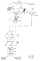
- FIG. 4 shows an embodiment of the invention, wherein 1' still represents one of the films, e.g. Fl on which the circuit tracks are designed f.i. graphically plotted.
- Fl preferably is a china ink master in a graduated scale from 1:1 to 4:1.
- a simple system for applying conducting material e.g. ink to copper
- the plotted upper surface of Fl is illuminated by a light source 21 (e.g. a flash) the rays of which 22 are reflected (as rays 23) to a system of lens 24, the output rays of which 25 are directed towards a drum (e.g. selenium) 26.
- a light source 21 e.g. a flash
- the rays of which 22 are reflected (as rays 23)
- a system of lens 24 the output rays of which 25 are directed towards a drum (e.g. selenium) 26.
- a drum e.g. selenium
- a metallic powder 27 is applied to the lines of said image.
- Said metallic powder must be colloidal state containing Cu, Ag, Zn and Au and able to attack only in the opposite electrostatic charge regions, i.g. exactly on the outlines of the image.
- the photostatic application is similar to the application of toner in a photostatic copying machine.
- the selenium drum 26 prints and fixes the metallic tracks on sheet FS1. Printing and fixing are repeated for sheet FS2 that carries the geometry of the soldering side.
- FS1 and FS2 are glued to the two major faces of a rigid support SR being much more thicker than sheets FS1 and FS2, e.g. by 0.5 to 20 mm.
- SR is a support obtained by compressing or injecting synthetic material, e.g. one or more (co) polymers of olefines, vinyl compounds, esters, amids, dichloroethylenes etc. Said materials have the advantage of being dielectric, stable etc. and may be treated on the surface to increase their adhesion to the printed sheets and to the section of tracks.
- synthetic material e.g. one or more (co) polymers of olefines, vinyl compounds, esters, amids, dichloroethylenes etc.
- Said materials have the advantage of being dielectric, stable etc. and may be treated on the surface to increase their adhesion to the printed sheets and to the section of tracks.
- the rigid support SR can also be metallic or partially metallic.
- SR is made of synthetic material, it shall be coupled to a board (e.g. in Al) with a high leakage of heat.
- FS2 has the further advantage of adopting rigid supports SR with such dimensions, compositions and structures that high heat leakages can be achiewed.
- Board PIAS goes out from 4' and is drilled with squared reference holes from CAM.
- the boards outgoing from 4" are treated in 4' to enlarge the section of conductors and upon having been tested in 40 they can be sent to the other working operations which will be exclusively mechanical in the event of boards for suface mounting without holes (41) or other mechanical, drilling or electrochemical processes if traditional pcb's with metallic holes are involved (42).
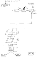
- F ig. 5 shows the preferred and most advantageous embodiment of the invention.
- the first three steps of the process of Fig. 2 i.e. the use of the CAD signal, its application to a graphic plotter, and the preparation of the ink plotted sheets Fl, F2 and F3 are eliminated by utilizing directly a digitalized graphic output UGD from a computer (not shown) and by applying this digital signal to a electrophotographic transfert unit UTEF (1") which transfers said graphic output directly to the photoconductor drum 26 11 (corresponding to drum 26 of fig. 4) whereby this last is able to receive the toner 27 and to give in step 2" the sheets FS1 and FS2.
- a digitalized graphic output UGD from a computer (not shown)
- a electrophotographic transfert unit UTEF (1" which transfers said graphic output directly to the photoconductor drum 26 11 (corresponding to drum 26 of fig. 4) whereby this last is able to receive the toner 27 and to give in step 2" the sheets FS1 and FS
- step 4' giving thus a board PIAS formed of the support SR bearing the said printed sheets FS1 and FS2 which undergo the treatment 4' (growing of the tracks), the final quality text 40, the convention workings 41 and the selection toward 41' pcb for surface mountings) and 42 (conventional pcb).
- Fig. 6 shows the scheme of a preferred embodiment of the transfer unit UTEF (1") of fig. 5: it comprises a control unit UCT of a cathode tube TCR (CRT) and of a scanning synchronization, 1" which delivers the signals to command the positioning on axis y (through line 20 and synchronizer SINC) of drum 26', and of the axis x (line 30) and z (line 40) of same drum by acting however on the rays outgoing from tube TRC (CRT) which throughan optical projection system SOP creates the labile image on drum 26'.
- a control unit UCT of a cathode tube TCR (CRT) and of a scanning synchronization, 1" which delivers the signals to command the positioning on axis y (through line 20 and synchronizer SINC) of drum 26', and of the axis x (line 30) and z (line 40) of same drum by acting however on the rays outgoing from tube TRC (CRT) which
- UCT comprises also a deflection unit 10" acting on TRC (CRT) throughline 50.
- CRT TRC
- the drum 26' undergoes operation 27 (toner application) and 2" (transfer of the toner tracks from 26 to print the sheets FSl - FS2).
Landscapes
- Engineering & Computer Science (AREA)
- Manufacturing & Machinery (AREA)
- Microelectronics & Electronic Packaging (AREA)
- Manufacturing Of Printed Wiring (AREA)
- Insulated Metal Substrates For Printed Circuits (AREA)
- Structure Of Printed Boards (AREA)
- Production Of Multi-Layered Print Wiring Board (AREA)
Applications Claiming Priority (2)
| Application Number | Priority Date | Filing Date | Title |
|---|---|---|---|
| IT8520284A IT1184408B (it) | 1985-04-09 | 1985-04-09 | Processo per la fabbricazione di piastre e circuiti stampati,e prodotti relativi |
| IT2028485 | 1985-04-09 |
Publications (2)
| Publication Number | Publication Date |
|---|---|
| EP0197276A2 true EP0197276A2 (fr) | 1986-10-15 |
| EP0197276A3 EP0197276A3 (fr) | 1987-05-20 |
Family
ID=11165423
Family Applications (1)
| Application Number | Title | Priority Date | Filing Date |
|---|---|---|---|
| EP86102413A Withdrawn EP0197276A3 (fr) | 1985-04-09 | 1986-02-25 | Procédé de fabrication de circuits imprimés et produits ainsi obtenus |
Country Status (5)
| Country | Link |
|---|---|
| US (1) | US4897326A (fr) |
| EP (1) | EP0197276A3 (fr) |
| JP (1) | JPH06105826B2 (fr) |
| ES (1) | ES8707069A1 (fr) |
| IT (1) | IT1184408B (fr) |
Cited By (1)
| Publication number | Priority date | Publication date | Assignee | Title |
|---|---|---|---|---|
| EP0373776A3 (fr) * | 1988-12-13 | 1991-03-20 | Minnesota Mining And Manufacturing Company | Dispersions liquides de toneur, images métalliques, et leur transfert thermique |
Families Citing this family (18)
| Publication number | Priority date | Publication date | Assignee | Title |
|---|---|---|---|---|
| JP2848830B2 (ja) * | 1988-09-02 | 1999-01-20 | 旭電化工業株式会社 | 水に難溶性の脂肪酸エステルの可溶化方法 |
| US5196286A (en) * | 1989-07-31 | 1993-03-23 | Watkins Roger D | Method for patterning a substrate |
| US5416569A (en) * | 1991-01-04 | 1995-05-16 | Goldberg; Michael | Electrographically making devices having electrically conductive paths corresponding to those graphically represented on a mask |
| DE4122326C1 (en) * | 1991-07-05 | 1993-02-04 | Rolf 7245 Starzach De Jethon | Three=dimensional shaped bodies prodn. - by putting powder on photosemiconductor by electrostatic force and transferring to workpiece support |
| JPH0888456A (ja) * | 1994-09-14 | 1996-04-02 | Nikon Corp | 基板配線製造方法および製造装置 |
| US6445969B1 (en) * | 1997-01-27 | 2002-09-03 | Circuit Image Systems | Statistical process control integration systems and methods for monitoring manufacturing processes |
| JPH11354371A (ja) * | 1998-06-04 | 1999-12-24 | Murata Mfg Co Ltd | セラミック電子部品の製造方法 |
| SE0000680D0 (sv) * | 2000-03-02 | 2000-03-02 | Array Printers Ab | Method and device for manufacturing printed circuit boards |
| WO2003059027A1 (fr) * | 2002-01-14 | 2003-07-17 | Fraunhofer-Gesellschaft zur Förderung der angewandten Forschung e.V. | Systeme de fabrication de circuits electriques et integres |
| JP2004048030A (ja) * | 2002-07-15 | 2004-02-12 | Toshiba Corp | 電子回路の製造方法および電子回路の製造装置 |
| JP2005050992A (ja) * | 2003-07-28 | 2005-02-24 | Toshiba Corp | 配線基板および多層配線基板 |
| JP4130407B2 (ja) * | 2003-12-26 | 2008-08-06 | 株式会社東芝 | 電子回路の製造方法 |
| JP2005195690A (ja) * | 2003-12-26 | 2005-07-21 | Toshiba Corp | 金属含有樹脂粒子、樹脂粒子、及び電子回路の製造方法 |
| TW200521171A (en) * | 2003-12-26 | 2005-07-01 | Toshiba Kk | Resin particles and resin layer containing metal micro particles, its forming method and circuit base board |
| JP2005203396A (ja) * | 2004-01-13 | 2005-07-28 | Toshiba Corp | 電子部品の製造装置、電子部品の製造方法および電子部品 |
| KR100645407B1 (ko) * | 2004-04-08 | 2006-11-14 | 가부시끼가이샤 도시바 | 화상 형성 장치와 그것을 이용한 전자 회로의 제조 방법 |
| JP4488784B2 (ja) * | 2004-04-13 | 2010-06-23 | 株式会社東芝 | 電子回路の製造方法および電子回路 |
| JP2005303090A (ja) * | 2004-04-13 | 2005-10-27 | Toshiba Corp | 配線基板および配線基板の製造方法 |
Family Cites Families (15)
| Publication number | Priority date | Publication date | Assignee | Title |
|---|---|---|---|---|
| US3275436A (en) * | 1962-07-24 | 1966-09-27 | Xerox Corp | Method of image reproduction utilizing a uniform releasable surface film |
| US3862352A (en) * | 1968-04-16 | 1975-01-21 | Itek Corp | Photographically prepared electrical circuits wherein the photosensitive material is a photoconductor |
| DE2006134A1 (de) * | 1969-02-17 | 1970-09-03 | Electro Connective Systems Inc., Brockton, Mass. (V.St.A. | Flexible gedruckte Schaltung sowie Verfahren und Vorrichtung zu ihrer Herstellung |
| US4066453A (en) * | 1973-05-02 | 1978-01-03 | Hoechst Aktiengesellschaft | Process for the preparation of printing forms |
| DE2556386C2 (de) * | 1975-12-15 | 1985-02-28 | Hoechst Ag, 6230 Frankfurt | Verfahren zur Herstellung von Druckformen und/oder metallisierten Bildern |
| JPS5437265A (en) * | 1977-08-30 | 1979-03-19 | Inoue Japax Res | Print wiring substrate |
| DK153337C (da) * | 1979-04-11 | 1988-11-14 | Platonec Aps | Fremgangsmaade til toer sensibilisering af en isolerende overflade |
| JPS56129394A (en) * | 1980-03-14 | 1981-10-09 | Dainippon Screen Mfg | Method of producing through hole of printed board |
| DE3024772A1 (de) * | 1980-06-30 | 1982-01-28 | Hoechst Ag, 6000 Frankfurt | Elastische, laminierbare lichtempfindliche schicht |
| DE3024718A1 (de) * | 1980-06-30 | 1982-01-28 | Hoechst Ag, 6000 Frankfurt | Verfahren zur herstellung von druckformen oder gedruckten schaltungen |
| DE3047498A1 (de) * | 1980-12-17 | 1982-07-22 | Herbert 4600 Dortmund Karnikowski | Uebertragungsfolie fuer die uebertragung von abbildungen auf oberflaechen, sowie uebertragungsverfahren und vorrichtung |
| US4439815A (en) * | 1982-02-01 | 1984-03-27 | International Telephone And Telegraph Corporation | Printed circuit assembly for a card file packaging system |
| US4467335A (en) * | 1982-05-07 | 1984-08-21 | Data Card Corporation | System for forming an image on the surface of a plastic card |
| JPS59112688A (ja) * | 1983-12-08 | 1984-06-29 | キヤノン株式会社 | 電子機器 |
| US4661431A (en) * | 1984-09-27 | 1987-04-28 | Olin Hunt Specialty Products, Inc. | Method of imaging resist patterns of high resolution on the surface of a conductor |
-
1985
- 1985-04-09 IT IT8520284A patent/IT1184408B/it active
-
1986
- 1986-02-25 EP EP86102413A patent/EP0197276A3/fr not_active Withdrawn
- 1986-03-03 US US06/835,479 patent/US4897326A/en not_active Expired - Fee Related
- 1986-03-06 ES ES552730A patent/ES8707069A1/es not_active Expired
- 1986-03-07 JP JP61048710A patent/JPH06105826B2/ja not_active Expired - Lifetime
Cited By (1)
| Publication number | Priority date | Publication date | Assignee | Title |
|---|---|---|---|---|
| EP0373776A3 (fr) * | 1988-12-13 | 1991-03-20 | Minnesota Mining And Manufacturing Company | Dispersions liquides de toneur, images métalliques, et leur transfert thermique |
Also Published As
| Publication number | Publication date |
|---|---|
| ES8707069A1 (es) | 1987-07-01 |
| IT8520284A0 (it) | 1985-04-09 |
| US4897326A (en) | 1990-01-30 |
| IT8520284A1 (it) | 1986-10-09 |
| JPH06105826B2 (ja) | 1994-12-21 |
| ES552730A0 (es) | 1987-07-01 |
| EP0197276A3 (fr) | 1987-05-20 |
| IT1184408B (it) | 1987-10-28 |
| JPS61269393A (ja) | 1986-11-28 |
Similar Documents
| Publication | Publication Date | Title |
|---|---|---|
| EP0197276A2 (fr) | Procédé de fabrication de circuits imprimés et produits ainsi obtenus | |
| US4706167A (en) | Circuit wiring disposed on solder mask coating | |
| US4528259A (en) | Printed wiring boards with solder mask over bare copper wires having large area thickened circuit pad connections | |
| KR940007800B1 (ko) | 인쇄 배선 기판용 레지스트 패터닝방법 | |
| US6507993B2 (en) | Polymer thick-film resistor printed on planar circuit board surface | |
| US20100044095A1 (en) | Via Stub Elimination | |
| US4720915A (en) | Printed circuit board and process for its manufacture | |
| US5015553A (en) | Method of patterning resist | |
| US6004734A (en) | Circuit board substrate for use in fabricating a circuit board on which is formed a light sensitive emulsion layer covering and in direct contact with photoresist | |
| JPH0785510B2 (ja) | プリント回路基板とその製造方法 | |
| JP3019503B2 (ja) | プリント配線板の製造方法 | |
| US3385702A (en) | Photomechanical method of making metallic patterns | |
| US5254435A (en) | Method of patterning resist | |
| US3574933A (en) | Method of making printed circuit boards with plated-through holes | |
| CN1021874C (zh) | 印刷线路板的图形抗蚀法 | |
| US4627005A (en) | Equal density distribution process | |
| US5234745A (en) | Method of forming an insulating layer on a printed circuit board | |
| EP0101994B1 (fr) | Procédé pour modifier des plaquettes à circuit imprimé | |
| GB2176942A (en) | Making printed circuit boards | |
| AU615430B2 (en) | Method of patterning resist | |
| JP2723744B2 (ja) | 印刷配線板の製造方法 | |
| JPH1079561A (ja) | 配線基板および配線基板の形成方法 | |
| CA1149967A (fr) | Chaine de production de circuits imprimes | |
| JPH02139993A (ja) | 印刷配線基板の製造方法 | |
| CN85107672A (zh) | 均匀分布密度的加工方法 |
Legal Events
| Date | Code | Title | Description |
|---|---|---|---|
| PUAI | Public reference made under article 153(3) epc to a published international application that has entered the european phase |
Free format text: ORIGINAL CODE: 0009012 |
|
| AK | Designated contracting states |
Kind code of ref document: A2 Designated state(s): AT BE CH DE FR GB LI NL SE |
|
| PUAL | Search report despatched |
Free format text: ORIGINAL CODE: 0009013 |
|
| AK | Designated contracting states |
Kind code of ref document: A3 Designated state(s): AT BE CH DE FR GB LI NL SE |
|
| 17P | Request for examination filed |
Effective date: 19871002 |
|
| 17Q | First examination report despatched |
Effective date: 19891212 |
|
| STAA | Information on the status of an ep patent application or granted ep patent |
Free format text: STATUS: THE APPLICATION IS DEEMED TO BE WITHDRAWN |
|
| 18D | Application deemed to be withdrawn |
Effective date: 19900424 |
|
| RIN1 | Information on inventor provided before grant (corrected) |
Inventor name: MARENGO, GIUSEPPE |