EP0197453B1 - Procédé pour améliorer la qualité d'image pour des signaux d'images codés par modulation d'impulsions codées - Google Patents
Procédé pour améliorer la qualité d'image pour des signaux d'images codés par modulation d'impulsions codées Download PDFInfo
- Publication number
- EP0197453B1 EP0197453B1 EP86104259A EP86104259A EP0197453B1 EP 0197453 B1 EP0197453 B1 EP 0197453B1 EP 86104259 A EP86104259 A EP 86104259A EP 86104259 A EP86104259 A EP 86104259A EP 0197453 B1 EP0197453 B1 EP 0197453B1
- Authority
- EP
- European Patent Office
- Prior art keywords
- value
- picture signal
- signal value
- dpcm
- values
- Prior art date
- Legal status (The legal status is an assumption and is not a legal conclusion. Google has not performed a legal analysis and makes no representation as to the accuracy of the status listed.)
- Expired
Links
- 238000000034 method Methods 0.000 title claims abstract description 22
- 238000012937 correction Methods 0.000 claims abstract description 39
- 238000013139 quantization Methods 0.000 claims abstract description 33
- 238000010586 diagram Methods 0.000 description 4
- 230000005540 biological transmission Effects 0.000 description 3
- 238000004364 calculation method Methods 0.000 description 3
- 230000003111 delayed effect Effects 0.000 description 3
- 230000000873 masking effect Effects 0.000 description 3
- 239000008186 active pharmaceutical agent Substances 0.000 description 1
- 238000013459 approach Methods 0.000 description 1
- 230000007423 decrease Effects 0.000 description 1
- 230000007547 defect Effects 0.000 description 1
- 230000002950 deficient Effects 0.000 description 1
- 238000011161 development Methods 0.000 description 1
- 230000018109 developmental process Effects 0.000 description 1
- 238000012546 transfer Methods 0.000 description 1
Images
Classifications
-
- H—ELECTRICITY
- H04—ELECTRIC COMMUNICATION TECHNIQUE
- H04N—PICTORIAL COMMUNICATION, e.g. TELEVISION
- H04N19/00—Methods or arrangements for coding, decoding, compressing or decompressing digital video signals
- H04N19/10—Methods or arrangements for coding, decoding, compressing or decompressing digital video signals using adaptive coding
- H04N19/102—Methods or arrangements for coding, decoding, compressing or decompressing digital video signals using adaptive coding characterised by the element, parameter or selection affected or controlled by the adaptive coding
- H04N19/124—Quantisation
-
- H—ELECTRICITY
- H04—ELECTRIC COMMUNICATION TECHNIQUE
- H04N—PICTORIAL COMMUNICATION, e.g. TELEVISION
- H04N19/00—Methods or arrangements for coding, decoding, compressing or decompressing digital video signals
- H04N19/50—Methods or arrangements for coding, decoding, compressing or decompressing digital video signals using predictive coding
Definitions
- the invention relates to a method for improving the image quality, in which digitized image signal values are converted into quantized DPCM values using a multidimensional, in particular a two-dimensional, prediction and switchable quantization characteristics.
- Differential pulse code modulation is often used to reduce the transmission rate when transmitting image signals.
- the most common is the two-dimensional DPCM, in which an estimate or prediction value is calculated from image signal values that adjoin the current image signal value to be processed.
- DPCM coding with two-dimensional prediction is already surprisingly powerful.
- a switch is made between several quantization characteristics, so that the quantization takes place in small quantization steps when there are small differences between the estimated value and the current image signal value; in the case of large differences, such as occur at edges, a coarser quantization is used, but the quantization error is largely invisible to the human eye due to the masking effect.
- the object of the invention is to provide a method for improving the image quality in DPCM-coded image signals, in which no change in the prediction algorithm on the transmitting and receiving side is necessary.
- the object is achieved in that at least one reconstructed image signal value is temporarily stored and outputted with a delay at the receiving end, and that when a DPCM value is received which corresponds to the maximum value of a quantization range of the quantization characteristic used, instead of with this DPCM -Value of the reconstructed image signal value, a correction value is output which has been determined from subsequent image signal values and, if appropriate, additionally from the image signal value to be corrected.
- the invention requires the knowledge that the DPCM values (differences) transmitted in DPCM coding with an insufficient amplitude can be easily recognized. Since the output of the reconstructed image signal values takes place with a delay, a correction value can be output instead of an image signal value falsified due to the DPCM coding, which is determined from the following reconstructed image signal values or at least predominantly from these. This is possible because the error decreases relatively quickly and is no longer noticeable after approximately the third reconstructed image signal value. In contrast to the previously known methods, the correction value is determined solely from the subsequent image signal values, possibly also additionally from the image signal value to be corrected, and not, as previously, from the previous or from previous and subsequent image signal values.
- the subsequent image signal value is output as a correction value.
- an interpolation value which was determined taking into account the subsequent image signal values adjacent to the buffered image signal value, is output as a correction value.
- the errors caused by the DPCM method for critical image structures can be further reduced. If the application of the method to font templates is restricted by including further decision criteria, the correction can be improved by taking greater account of the image signal values which are further from the critical image signal value. As a result, high contrasts between adjacent pixels are achieved. However, a moderate correction can also be carried out, which reproduces the original with sufficient precision and is less disruptive when errors are interpreted.
- the signs of the differences between the temporarily stored image signal value and the subsequent image signal value as well as the previously stored image signal value and the temporarily stored image signal value and the temporarily stored image signal value are determined and that a correction is only carried out with the same sign and that the sign is only corrected.
- the image signal value which belongs to the image signal value lying before the temporarily stored image signal value is compared with a minimum value and that a correction is only carried out if this DPCM value is smaller than this minimum value.
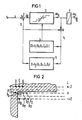
- the encoder input 1 is connected via a subtractor 2 to the input of a controllable quantizer 3, the output of which is connected to an encoder 7, the output of which is designated by 10.
- the output of the quantizer 3 is connected to the first input of an adder 6, to the output of which a quantizer control logic 4 and a predictor 5 are connected, the output of which is connected to the second input of the adder 6 and to the subtraction input of the subtractor 2.
- the digitized image signal values s are supplied to the code input 1. By comparing it with the estimated values at the subtraction input of the subtractor 2, DPCM values A s are calculated, which are converted into quantized DPCM values AS q (differences) in accordance with the quantization characteristic curve set by the quantizer control logic 4.
- the quantization stages are assigned certain binary combinations by the encoder 7, which correspond to the quantized DPCM values and are transmitted at the encoder output 10 as coded DPCM values A s c .
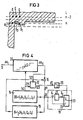
- Fig. 2 For the calculation of an estimate or prediction value applies, for example (Fig. 2):
- the quantization characteristic is determined by the reconstructed image signal values sr, which are present at the output of the adder 6.
- the quantizer is controlled by the greatest difference between adjacent reconstructed image signal values A r to D r (FIG. 2).
- FIG. 2 shows a picture structure which is critical for DPCM coding, as occurs particularly frequently in the transmission of typeface publishers.
- the reconstructed image signal values A r , B r , C r and D r used for the prediction and control of the quantization characteristic are still in the black area, corresponding to the original image signal values, while the current image signal value Xo to be transmitted is in the upper left corner of a white field .
- the black image signal values correspond to the value 0, the white image signal values should correspond to the value 255 here.
- Equation 2 there is a difference of zero or a very small difference, so that the first quantization characteristic QK1 is used in the coding of the DPCM value and thus a maximum DPCM value of 55 is transmitted instead of a maximum possible DPCM value of 120 according to the quantization characteristic 4.
- a DPCM A value of 255 is necessary, but a masking effect also occurs in the human eye at high contrasts, which makes a DPCM value of 120 appear sufficient.
- a conventional DPCM decoder is used at the receiving end, in which control logic and a correction device are added.
- the DPCM decoder shown in FIG. 4 contains a decoding device 37, the input of which is supplied via the decoder input 11 with the coded PCM values A s c .
- the output of the decoder 37 is connected to the first input of an adder 16, the output of which is connected to the input of a quantization control logic 14 at the receiving end and a predictor 15, the output of which is fed back to the second input of the adder 16.
- the reconstructed image signal values sr are output at the output of the adder 16.
- a correction device 19 is connected to the DPCM decoder output 20. It contains a memory 21 serving as a delay element, the output and input of which are each connected to an input of a changeover switch 22. The output of the switch forms the output 23 of the correction device.
- a control logic 12 is provided, the first input 121 of which is connected to the output of the quantization control logic 14 and the second input 122 of which is connected to the output of the decoding device 37 (or also to its input).
- the output 123 is led via a delay element 39 to the control input of the changeover switch 22.
- This check can be carried out by comparing the signs of the quantized DPCM values A sq or the coded DPCM values A s c (a change of sign can also be permitted under certain circumstances if the amount of the difference Xo-Xi is below a predetermined threshold value). If a correction is to be carried out, the correction signal KS output at the output 123 of the control logic is delayed via the delay element 39 until the image signal value Xo, which is recognized as being defective, is present at the output of the memory 21. If the delay time of the correction stage corresponds only to the distance between two received DPCM values, the runtime element 39 is not required. If the conditions for a correction for the next reconstructed image signal value Xi are also fulfilled, then this is also replaced by the next image signal value X 2 .
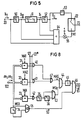
- a circuit arrangement for determining the correction value XK1 is shown in FIG. 5. It essentially contains a series connection of 3 delay elements 50, 51 and 52 whose inputs and outputs are connected to the inputs of an adder 54, the output of which is led via a multiplier 55 to the first input of the changeover switch 22.
- the output of the delay element 52 is connected to the second input of the switch 22 via a further delay element 53.
- the delay elements 50 and 52 each delay by a clock pulse which corresponds to the distance when two DPCM values are received.
- the middle delay element 51 has the delay ⁇ Z- ⁇ 1 of a picture line (television line) except for one clock pulse.
- the sum of the image signal values X o , X i , X i o and X ii present at the outputs of the delay elements 52, 51, 50 and at the input of the delay element is formed in the adder 54.
- the multiplier 55 is implemented by suitable wiring between the output of the adder 55 and the first input of the changeover switch 22.
- the delay element 53 provided to compensate for the addition time is generally not required.
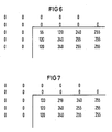
- Each image signal value shown in Fig. 2 is a numerical value assigned.
- the image signal values of the black image part correspond to the numerical value zero, the image signal values of the white image part with a maximum possible contrast are assigned the numerical value 255.
- 6 and 7 the numerical values for the reconstructed image signal values are given.
- the maximum possible image signal value of 55 is transmitted with the quantization characteristic QK1.
- the quantization characteristic QK2 transmits the maximum possible numerical value of 65, etc.
- the third reconstructed image signal value X3 has practically reached the correct image signal value of 255.
- the reconstructed image signal values approach the original image signal value more quickly. Due to the masking effect of the human eye, an image signal value of 120 instead of correctly 255 is already accepted as almost correct.
- the table according to FIG. 7 shows the image signal values which result from interpolation according to equation (3). The particularly sensitively disturbed image signal value Xo has already been corrected sufficiently.
- the image signal values of the first column of the white part of the image can be further improved by using a different interpolation algorithm.
- FIG. 8 An exemplary embodiment for the control logic 12 is shown in FIG. 8. It is assumed that the critical image signal values should be corrected whenever the maximum value MA1 of the first quantization characteristic QK1 or the maximum value MA2 of the second quantization characteristic QK2 is received.
- the inputs of three comparators 31, 32 and 33 are connected to the input 122 of the control logic, the comparison inputs of which are supplied with the maximum values MA1, MA2 and a minimum value MIN.
- the outputs of the comparators are each guided via an AND gate 40, 41 and 42.
- the second inputs of the AND gates 40 and 42 are connected to the input 121 of the control logic, the input of the AND gate 41 is connected to an input 21 * .
- the AND gates 40 and 41 are guided via an OR gate 47 to a further AND gate 44, while the output of the third AND gate 42 via two delay elements 36 and 38 and via an OR gate 43 - the inputs of which are in each case connected to an output of these delay elements - are connected to the third input of the AND gate 44.
- the output of the AND gate 44 is connected via a further delay element 45 to a further AND gate 46, the output 230 of which corresponds to the output 23 of the control logic shown in FIG. 4.
- the sign bit MSB of the DPCM value present at input 122 is connected directly and via a delay element 34 to the inputs of an EXCLUSIVE NOR gate 35, the output of which is connected to the second input of AND gate 46.
- the comparators 31 and 32 and their downstream AND gates 40 and 41 are used to check whether a maximum value MA1 or MA2 is present with the correspondingly set quantization characteristic (inputs 121, 21 *).
- the third comparator 33 has already checked whether the amounts of the DPCM values already received were below the minimum MIN (or at zero), as is the case for example with text templates. The result of this check is delayed via the delay elements 36 and 38, so that it is present in the case of a correction decision for the critical image signal values Xo and X 1 .
- This minimum signal MS is logically combined with a maximum signal MAS via the AND gate 44 and delayed by one clock pulse via the delay element 45.
- the EXCLUSIVE NOR gate 35 is used to check whether the sign of the DPCM values associated with the image signal values X o and Xi changes. If this is not the case, the sign signal SG is logically linked via the AND gate 46. When all the conditions already described occur, a correction signal KS is emitted at the output of the AND gate 46, which actuates the changeover switch 23.
- control logic can be adapted to the interpolation algorithm used in each case and to the respective correction conditions without difficulty. It is of course also possible to evaluate the coded DPCM values A s c instead of the quantized DPCM values A sq. Under certain circumstances, the AND gates 40, 41 and 42 can also be dispensed with here.
Landscapes
- Engineering & Computer Science (AREA)
- Multimedia (AREA)
- Signal Processing (AREA)
- Compression Or Coding Systems Of Tv Signals (AREA)
- Compression, Expansion, Code Conversion, And Decoders (AREA)
Claims (10)

Priority Applications (1)
| Application Number | Priority Date | Filing Date | Title |
|---|---|---|---|
| AT86104259T ATE45656T1 (de) | 1985-03-29 | 1986-03-27 | Verfahren zur verbesserung der bildqualitaet bei dpcm-codierten bildsignalen. |
Applications Claiming Priority (2)
| Application Number | Priority Date | Filing Date | Title |
|---|---|---|---|
| DE19853511714 DE3511714A1 (de) | 1985-03-29 | 1985-03-29 | Verfahren zur verbesserung der bildqualitaet |
| DE3511714 | 1985-03-29 |
Publications (2)
| Publication Number | Publication Date |
|---|---|
| EP0197453A1 EP0197453A1 (fr) | 1986-10-15 |
| EP0197453B1 true EP0197453B1 (fr) | 1989-08-16 |
Family
ID=6266877
Family Applications (1)
| Application Number | Title | Priority Date | Filing Date |
|---|---|---|---|
| EP86104259A Expired EP0197453B1 (fr) | 1985-03-29 | 1986-03-27 | Procédé pour améliorer la qualité d'image pour des signaux d'images codés par modulation d'impulsions codées |
Country Status (3)
| Country | Link |
|---|---|
| EP (1) | EP0197453B1 (fr) |
| AT (1) | ATE45656T1 (fr) |
| DE (2) | DE3511714A1 (fr) |
Family Cites Families (5)
| Publication number | Priority date | Publication date | Assignee | Title |
|---|---|---|---|---|
| DE2559263C3 (de) * | 1975-12-31 | 1980-07-31 | Deutsche Forschungs- Und Versuchsanstalt Fuer Luft- Und Raumfahrt E.V., 5000 Koeln | Ausgleich von Quantisierungsverzerrungen bei Bildcodierung mit Blockquantisierung |
| US4430670A (en) * | 1982-03-12 | 1984-02-07 | Bell Telephone Laboratories, Incorporated | Reconstruction of quantized DPCM or PCM signals |
| GB2121642B (en) * | 1982-05-26 | 1985-11-27 | Sony Corp | Error concealment in digital television signals |
| FR2532138B1 (fr) * | 1982-08-20 | 1986-10-10 | Thomson Csf | Procede de compression de debit de donnees successivement transmises entre un emetteur et un recepteur de television et systeme mettant en oeuvre le procede |
| DE3311911A1 (de) * | 1983-03-31 | 1984-10-04 | Siemens AG, 1000 Berlin und 8000 München | Verfahren und schaltungsanordnung zur bildfehlerkorrektur |
-
1985
- 1985-03-29 DE DE19853511714 patent/DE3511714A1/de not_active Withdrawn
-
1986
- 1986-03-27 EP EP86104259A patent/EP0197453B1/fr not_active Expired
- 1986-03-27 DE DE8686104259T patent/DE3665121D1/de not_active Expired
- 1986-03-27 AT AT86104259T patent/ATE45656T1/de not_active IP Right Cessation
Also Published As
| Publication number | Publication date |
|---|---|
| DE3665121D1 (en) | 1989-09-21 |
| DE3511714A1 (de) | 1986-10-09 |
| EP0197453A1 (fr) | 1986-10-15 |
| ATE45656T1 (de) | 1989-09-15 |
Similar Documents
| Publication | Publication Date | Title |
|---|---|---|
| DE2225652C3 (de) | Verfahren und Einrichtung zur Codierung und Decodierung von Videosignalen | |
| DE3636675C2 (fr) | ||
| DE3784617T2 (de) | Digital-analog-wandler. | |
| DE3134703C2 (fr) | ||
| EP0123893B1 (fr) | Procédé et circuit pour la correction des erreurs d'image | |
| DE3331426A1 (de) | Anordnung zur zweidimensionalen dpcm-codierung | |
| DE2156673C3 (de) | Anordnung zur Behandlung eines Fernsehsignals | |
| DE1925978C2 (de) | System zur Reduzierung der Bandbreite bei der Übertragung eines analogen Impulssignals | |
| DE3426939A1 (de) | Einbettungsquantisierungsvorrichtung fuer ein vektorsignal | |
| DE3885303T2 (de) | Verfahren zur annäherung eines wertes, der eine nichtlineare funktion der linearen bildelementsdatenmittelwerte ist. | |
| DE3688579T2 (de) | Vorrichtung und verfahren zum verarbeiten von frueher verarbeiteten videosignalen. | |
| DE2826450C3 (de) | Verfahren zum Steuern der Übertragung digitaler Signale und Anordnung zur Durchführung des Verfahrens bei einer digitalen Faksimileübertragungseinrichtung | |
| EP0414016A2 (fr) | Procédé pour former les images de prédiction | |
| DE3140825C2 (fr) | ||
| DE3311898C2 (de) | Verfahren zur Störsignalreduktion von digitalen datenreduzierten Fernsehsignalen | |
| EP0189860B1 (fr) | Méthode de correction d'erreurs d'image | |
| DE69021274T2 (de) | Anordnung zum Detektieren von Nulldurchgängen. | |
| EP0197446A1 (fr) | Procédé pour améliorer la qualité d'image pour des signaux d'images codés par modulation d'impulsions codées | |
| DE2419279A1 (de) | Fernsehsystem | |
| EP0197453A1 (fr) | Procédé pour améliorer la qualité d'image pour des signaux d'images codés par modulation d'impulsions codées | |
| DE2850857A1 (de) | Gammakorrekturschaltung fuer fernsehen | |
| DE2539428A1 (de) | Informationsanzeigeeinrichtung | |
| DE4225508C2 (de) | Verfahren und Schaltungsanordnung zur Kontraststeigerung | |
| DE2364629C2 (de) | System zur Codierung von Video-Signalen nach dem sogenannten Differenzsignalverfahren | |
| DE4319376C1 (de) | Anordnung zur Analog/Digital-Wandlung von Signalen mit unterschiedlichem Signalpegel |
Legal Events
| Date | Code | Title | Description |
|---|---|---|---|
| PUAI | Public reference made under article 153(3) epc to a published international application that has entered the european phase |
Free format text: ORIGINAL CODE: 0009012 |
|
| AK | Designated contracting states |
Kind code of ref document: A1 Designated state(s): AT BE CH DE FR GB IT LI NL SE |
|
| 17P | Request for examination filed |
Effective date: 19861106 |
|
| 17Q | First examination report despatched |
Effective date: 19880622 |
|
| GRAA | (expected) grant |
Free format text: ORIGINAL CODE: 0009210 |
|
| AK | Designated contracting states |
Kind code of ref document: B1 Designated state(s): AT BE CH DE FR GB IT LI NL SE |
|
| REF | Corresponds to: |
Ref document number: 45656 Country of ref document: AT Date of ref document: 19890915 Kind code of ref document: T |
|
| REF | Corresponds to: |
Ref document number: 3665121 Country of ref document: DE Date of ref document: 19890921 |
|
| ET | Fr: translation filed | ||
| ITF | It: translation for a ep patent filed | ||
| GBT | Gb: translation of ep patent filed (gb section 77(6)(a)/1977) | ||
| PGFP | Annual fee paid to national office [announced via postgrant information from national office to epo] |
Ref country code: GB Payment date: 19900228 Year of fee payment: 5 |
|
| PGFP | Annual fee paid to national office [announced via postgrant information from national office to epo] |
Ref country code: AT Payment date: 19900302 Year of fee payment: 5 |
|
| PGFP | Annual fee paid to national office [announced via postgrant information from national office to epo] |
Ref country code: BE Payment date: 19900316 Year of fee payment: 5 |
|
| PGFP | Annual fee paid to national office [announced via postgrant information from national office to epo] |
Ref country code: FR Payment date: 19900321 Year of fee payment: 5 |
|
| PGFP | Annual fee paid to national office [announced via postgrant information from national office to epo] |
Ref country code: SE Payment date: 19900323 Year of fee payment: 5 |
|
| ITTA | It: last paid annual fee | ||
| PGFP | Annual fee paid to national office [announced via postgrant information from national office to epo] |
Ref country code: NL Payment date: 19900331 Year of fee payment: 5 |
|
| PLBE | No opposition filed within time limit |
Free format text: ORIGINAL CODE: 0009261 |
|
| STAA | Information on the status of an ep patent application or granted ep patent |
Free format text: STATUS: NO OPPOSITION FILED WITHIN TIME LIMIT |
|
| PGFP | Annual fee paid to national office [announced via postgrant information from national office to epo] |
Ref country code: CH Payment date: 19900622 Year of fee payment: 5 |
|
| 26N | No opposition filed | ||
| PG25 | Lapsed in a contracting state [announced via postgrant information from national office to epo] |
Ref country code: GB Effective date: 19910327 Ref country code: AT Effective date: 19910327 |
|
| PG25 | Lapsed in a contracting state [announced via postgrant information from national office to epo] |
Ref country code: SE Effective date: 19910328 |
|
| PG25 | Lapsed in a contracting state [announced via postgrant information from national office to epo] |
Ref country code: LI Effective date: 19910331 Ref country code: CH Effective date: 19910331 Ref country code: BE Effective date: 19910331 |
|
| BERE | Be: lapsed |
Owner name: SIEMENS A.G. Effective date: 19910331 |
|
| PG25 | Lapsed in a contracting state [announced via postgrant information from national office to epo] |
Ref country code: NL Effective date: 19911001 |
|
| NLV4 | Nl: lapsed or anulled due to non-payment of the annual fee | ||
| GBPC | Gb: european patent ceased through non-payment of renewal fee | ||
| PG25 | Lapsed in a contracting state [announced via postgrant information from national office to epo] |
Ref country code: FR Effective date: 19911129 |
|
| REG | Reference to a national code |
Ref country code: CH Ref legal event code: PL |
|
| REG | Reference to a national code |
Ref country code: FR Ref legal event code: ST |
|
| EUG | Se: european patent has lapsed |
Ref document number: 86104259.6 Effective date: 19911009 |
|
| PGFP | Annual fee paid to national office [announced via postgrant information from national office to epo] |
Ref country code: DE Payment date: 19960520 Year of fee payment: 11 |
|
| PG25 | Lapsed in a contracting state [announced via postgrant information from national office to epo] |
Ref country code: DE Effective date: 19971202 |
|
| PG25 | Lapsed in a contracting state [announced via postgrant information from national office to epo] |
Ref country code: IT Free format text: LAPSE BECAUSE OF NON-PAYMENT OF DUE FEES;WARNING: LAPSES OF ITALIAN PATENTS WITH EFFECTIVE DATE BEFORE 2007 MAY HAVE OCCURRED AT ANY TIME BEFORE 2007. THE CORRECT EFFECTIVE DATE MAY BE DIFFERENT FROM THE ONE RECORDED. Effective date: 20050327 |