EP0197658A2 - Commutateur à MOSFET pour courant alternatif - Google Patents
Commutateur à MOSFET pour courant alternatif Download PDFInfo
- Publication number
- EP0197658A2 EP0197658A2 EP86301654A EP86301654A EP0197658A2 EP 0197658 A2 EP0197658 A2 EP 0197658A2 EP 86301654 A EP86301654 A EP 86301654A EP 86301654 A EP86301654 A EP 86301654A EP 0197658 A2 EP0197658 A2 EP 0197658A2
- Authority
- EP
- European Patent Office
- Prior art keywords
- source
- switch means
- gate
- operatively connected
- load
- Prior art date
- Legal status (The legal status is an assumption and is not a legal conclusion. Google has not performed a legal analysis and makes no representation as to the accuracy of the status listed.)
- Granted
Links
Images

Classifications
-
- H—ELECTRICITY
- H03—ELECTRONIC CIRCUITRY
- H03K—PULSE TECHNIQUE
- H03K17/00—Electronic switching or gating, i.e. not by contact-making and –breaking
- H03K17/13—Modifications for switching at zero crossing
- H03K17/133—Modifications for switching at zero crossing in field-effect transistor switches
-
- H—ELECTRICITY
- H03—ELECTRONIC CIRCUITRY
- H03K—PULSE TECHNIQUE
- H03K17/00—Electronic switching or gating, i.e. not by contact-making and –breaking
- H03K17/51—Electronic switching or gating, i.e. not by contact-making and –breaking characterised by the components used
- H03K17/56—Electronic switching or gating, i.e. not by contact-making and –breaking characterised by the components used by the use, as active elements, of semiconductor devices
- H03K17/687—Electronic switching or gating, i.e. not by contact-making and –breaking characterised by the components used by the use, as active elements, of semiconductor devices the devices being field-effect transistors
- H03K17/6871—Electronic switching or gating, i.e. not by contact-making and –breaking characterised by the components used by the use, as active elements, of semiconductor devices the devices being field-effect transistors the output circuit comprising more than one controlled field-effect transistor
- H03K17/6874—Electronic switching or gating, i.e. not by contact-making and –breaking characterised by the components used by the use, as active elements, of semiconductor devices the devices being field-effect transistors the output circuit comprising more than one controlled field-effect transistor in a symmetrical configuration
Definitions
- the present invention relates in general to solid state relays and, in particular, to solid state relays and AC switches using MOSFET devices.
- solid state relays Compared to electromechanical relays, solid state relays have several advantages. These advantages include a longer lifetime, the elimination of contact bounce, and low voltage turn on that reduces both the electromagnetic interference and stress on the attached load.
- Typical prior art solid state relays utilize triac and SCR components for the switching device. These components when used in a solid state relay have a number of disadvantages. These solid state relays usually are very costly to manufacture, have high leakage current, and are prone to false triggering. Also prior art solid state relays are not readily compatible for use with high impedance logic circuits and CMOS logic.
- the present invention overcomes the drawbacks in the prior art solid state relays by the novel use of MOSFET devices.
- the present invention involves a solid state relay responding to a control signal and for use with an impedance load and a source of alternating electrical power.
- The-control signal is used to indicate when the solid state relay is to connect the impedance load to the source.
- the solid state relay uses two MOSFET devices wired in series in a source to source configuration. The load is connected in series with the MOSFET devices and the total series circuit is connected across the AC source. A portion of the circuitry in the solid state relay operates to turn on the solid state relay in response to the control signal and to a zero voltage crossing of the alternating electrical power of the source. Another portion of the circuitry of the solid state relay provides for turning off the solid state relay responsive to the control signal and to a zero current crossing of the alternating electrical current flowing through the load.
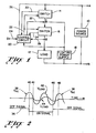
- the novel solid state relay of the present invention is shown in general block diagram form in Figure 1.
- An alternating power source 10 is connected between a hot node A and a neutral node N.
- An impedance load 12 is connected between node B and node N.
- a first switch 14 is connected in series with a second switch 16 at common node C and the combination is connected between nodes A and B and in series with the load 12.
- a floating power supply 18 is referenced to node C and provides a voltage to power the control circuit 20.
- the control circuit 20 controls the first and second switches 14 and 16 on output line 22.
- the control circuit 20 receives a control signal on input line 24 from terminal D.
- This control signal typically may be of the type from MIOS logic circuitry.
- the control circuit 20 monitors the voltage across switches 14 and 16 through lines 26 and 28 which are connected to nodes A and B respectively. Also the control circuit 20 monitors the current through switch 14 by lines 30 and 32 and monitors the current through switch 16 by lines 34 and 32.
- the control means 20 turns on switches 14 and 16 thereby connecting the load to the alternating source 10 in response to the control signal received at terminal D and to a substantially zero voltage crossing of the alternating electrical power of the source 10.
- the control means 20 turns off switches 14 and 16 in response to the control signal received on terminal D and to a substantially zero current crossing of the alternating electrical power source 10.
- Data signal 36 may be a typical logic signal operating between two low voltage levels. For one voltage level the signal indicates an off state for the solid state relay and for a second voltage level the signal indicates an on state for the solid state relay.
- Curve 38 illustrates the varying voltage of the power source 10.
- the solid state relay receives a data signal 36 indicating that the solid state relay is to turn on. However, the solid state relay does not turn on until time point 41 where the voltage 38 of the power source 10 crosses the zero axis.
- the solid state relay turns on connecting the load 12 to the source 10.
- Curves 42 and 44 show the voltage across the load 12 and the current through the load 12, respectively.
- the load 12 has been chosen to have a current which is out of phase with the voltage.
- the data signal 36 instructs the solid state relay to turn off.
- the solid state relay does not turn off until time point 48 when the current through the load 44 crosses the zero point.
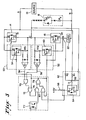
- Figure 3 is a more detailed block diagram of the present invention including circuit elements within each of the blocks.
- the first switch 14 and the second switch 16 are field effect transistors (FET) connected in a source to source configuration.
- the sources of FETs 14 and 16 are connected to node C, the drain of FET 14 is connected to node A and the drain of FET 16 is connected to node B.
- the gate of FET 14 is connected to the gate of FET 16.
- First and second current sensing circuits 50 and 52 are provided.
- FET 54 has its drain connected to the drain of FET 14 and its gate connected to the gate of FET 14.
- the source of FET 54 is connected to the source of FET 14 through series resistor RS1.
- RS1 series resistor
- An output signal from amplifier Q1 appears at the output 56 of the current sensing circuit 50 during the positive half cycle of the AC signal from the source 10 when the solid state relay is on.
- Operation of the second current sensing circuit 52 is similar to the operation described for the first current sensing circuit 50 and the output signal from Q2 which measures the voltage across RS2 and, therefore the current through FET 16, provides an output signal on the output 58 of the second current sensing circuit 52 during the negative half cycle of the AC signal from the source 10.
- FETs 54 and 60 provide high voltage protection for amplifiers Q1 and Q2.
- Voltage sensing circuit 62 is provided and has first and second resistors Rl and R2 connected between node A and node X, and between node B and node X, respectively.
- the floating power supply 18 provides a reference voltage to node X through R3.
- Node X is also connected to the gate of FET 64 which has its source connected to the floating power supply 18 and has its drain connected to an output terminal 66.
- Logic circuit 68 is provided and in the preferred embodiment has an OR gate 70 which has its inputs connected to terminals 56 and 58 of the first and second current sensing circuits 50 and 52, respectively.
- the output of the OR gate 70 is connected to one input of an AND gate 72 and the output of AND gate 72 is connected one input of an OR gate 76.
- the other input of OR gate 76 is connected to an optical isolator 77 which receives the control signal from terminal D.
- the output of OR gate 76 is connected to one input of AND gate 78.
- the other input of AND gate 78 is connected to the output of OR gate 80.
- OR gate 80 One input of OR gate 80 is connected to terminal 66 of the voltage sensing circuit 62 for receiving a voltage sensing signal and the other input of OR gate 80- is connected to the output AND gate 78. Similarly, the other input of AND gate 72 is connected to the output of AND gate 78. The output of AND gate 78 is also connected to the gates of FET 54 and 60 and in the first and second current sensing circuits 50 and 52, as well as, to the gates of the first and second FET switches 14 and 16. The overall operation of the circuit will now be described.
- FETs 14, 16, 54 and 60 are all also in the off state.
- the AC signal from the source 10 across FETs 14 and 16 is blocked because of internal diodes Dl and D2.
- the relay is on all four FET devices 14, 16, 54 and 60 are on and FETs 14 and 16 therefore create a short circuit connecting the load 22 to the source 10 across nodes A and N.
- the relay turns on only at substantially zero voltage crossing of the source 10 and the relay turns off only at substantially zero current crossings of the source 10.
- amplifier Ql When the relay is in the on state amplifier Ql outputs a signal during the positive half cycle of the AC signal of the source 10 and amplifier Q2 outputs a signal during the negative half cycle of the source 10.
- Amplifier Ql turns off only when the voltage drop across RS1 approaches zero, that is when the current flow through FET 14 approaches zero.
- amplifier Q2 turns off only at the same time as amplifier Q1, that is when the voltage across RS2 approaches zero which is when the current through FET 16 approaches zero.
- FET 54 and 60 can be turned on only when the output of AND gate 78 is high.
- the outputs of amplifiers Ql and Q2 drop to a low the input to AND gate 72 through OR gate 70 becomes low thereby providing an output from AND gate 72 which is low if the input to OR gate 76 from the optical coupler 77 is low, in addition to the signal from the output from AND gate 72 being low. In this case the output of OR gate 76 will be low.
- OR gate 76 If the input to AND gate 78 is low from OR gate 76 then the output of AND gate 78 will be low, thereby causing FET 54, 60, 14 and 16 to turn off.
- the input to OR gate 76 from the optical coupler 77 is low only when the data input on terminal D to the control circuit 20 is low, thereby indicating that the relay should turn off.
- the voltage appearing at node X in the voltage sensing circuit 62 is a full wave rectification of the AC signal from the source 10. This is formed by the voltage divider network R1 and R2 connected across nodes A and B. Thus, the voltage at node X is a sign wave of whose amplitude is about one-fifth the value of the AC signal in phase with the AC signal.
- the voltage across the gate and source of FET 64 is a whole wave rectified sign wave which is positive going. See Figures 4a and 4b.
- the voltage across the gate and source of FET 64 (V xc in Figure 4b) is viewed by comparing the voltage at node C to Node X (v c in Figure 4a) and the voltage at node X to node N (v x in Figure 4a).
- FET 64 is turned on except for the brief period (in the preferred embodiment approximately 200 microseconds) when the voltage from the gate to source of FET 64 drops to substantially the zero crossing point (V zc in Figure 4b). At this time the input to OR gate 80 connected to the terminal 66 goes high. At all other times the input to OR gate 80 from terminal 66 remains low.
Landscapes
- Electronic Switches (AREA)
Applications Claiming Priority (2)
| Application Number | Priority Date | Filing Date | Title |
|---|---|---|---|
| US719110 | 1985-04-02 | ||
| US06/719,110 US4680490A (en) | 1985-04-02 | 1985-04-02 | MOSFET AC switch |
Publications (3)
| Publication Number | Publication Date |
|---|---|
| EP0197658A2 true EP0197658A2 (fr) | 1986-10-15 |
| EP0197658A3 EP0197658A3 (en) | 1989-10-18 |
| EP0197658B1 EP0197658B1 (fr) | 1993-05-19 |
Family
ID=24888790
Family Applications (1)
| Application Number | Title | Priority Date | Filing Date |
|---|---|---|---|
| EP86301654A Expired - Lifetime EP0197658B1 (fr) | 1985-04-02 | 1986-03-07 | Commutateur à MOSFET pour courant alternatif |
Country Status (4)
| Country | Link |
|---|---|
| US (1) | US4680490A (fr) |
| EP (1) | EP0197658B1 (fr) |
| JP (1) | JP2690074B2 (fr) |
| DE (1) | DE3688438T2 (fr) |
Cited By (13)
| Publication number | Priority date | Publication date | Assignee | Title |
|---|---|---|---|---|
| EP0416522A3 (en) * | 1989-09-08 | 1992-04-01 | Telefunken Electronic Gmbh | Circuit for processing symmetrical signals |
| FR2871627A1 (fr) * | 2004-06-10 | 2005-12-16 | Goodrich Corp | Relais a l'etat solide pour la commutation d'une alimentation en alternatif vers une charge reactive et procede pour faire fonctionner un tel relais |
| US7196435B2 (en) | 2003-04-03 | 2007-03-27 | Goodrich Corporation | Solid state relay and method of operating the same |
| GB2493883A (en) * | 2010-07-06 | 2013-02-20 | Square R Llc V | System and method for regulating RMS voltage delivered to a load |
| DE102015211625A1 (de) | 2015-06-23 | 2016-12-29 | Phoenix Contact Gmbh & Co. Kg | Reversible elektronische Schutzschalterklemme |
| EP3343613A1 (fr) * | 2016-12-27 | 2018-07-04 | Renesas Electronics Corporation | Dispositif semi-conducteur et dispositif de protection contre les surintensités de courant |
| EP2339749B1 (fr) * | 2009-12-17 | 2018-10-24 | Hamilton Sundstrand Corporation | Interrupteur de courant alternatif à l'état solide |
| US10411694B2 (en) | 2016-07-22 | 2019-09-10 | Abb Schweiz Ag | Solid state switch system |
| US10554201B2 (en) | 2016-07-22 | 2020-02-04 | Abb Schweiz Ag | Solid state switch system |
| US11469757B2 (en) | 2020-10-16 | 2022-10-11 | Abb Schweiz Ag | Solid-state power switch |
| US11955900B2 (en) | 2021-06-30 | 2024-04-09 | Abb Schweiz Ag | Soft turn-off for motor controllers |
| US12074209B2 (en) | 2021-09-08 | 2024-08-27 | Abb Schweiz Ag | Sensor-less overcurrent fault detection using high electron mobility transistors |
| US12119817B2 (en) | 2021-12-13 | 2024-10-15 | Abb Schweiz Ag | Gate driver circuits with independently tunable performance characteristics |
Families Citing this family (29)
| Publication number | Priority date | Publication date | Assignee | Title |
|---|---|---|---|---|
| JPH0648447B2 (ja) * | 1987-10-21 | 1994-06-22 | 株式会社東芝 | 温度制御装置 |
| US4931844A (en) * | 1988-03-09 | 1990-06-05 | Ixys Corporation | High power transistor with voltage, current, power, resistance, and temperature sensing capability |
| JP2661167B2 (ja) * | 1988-04-18 | 1997-10-08 | 富士電機株式会社 | 半導体スイッチの電流零点遮断制御方法 |
| US5159425A (en) * | 1988-06-08 | 1992-10-27 | Ixys Corporation | Insulated gate device with current mirror having bi-directional capability |
| US5032745A (en) * | 1989-02-22 | 1991-07-16 | National Semiconductor Corporation | Current sensing of DC or a stepper motor |
| JP2536919B2 (ja) * | 1989-03-03 | 1996-09-25 | 富士電機株式会社 | 交流スイッチの電流零点遮断制御回路 |
| US5004969A (en) * | 1989-10-16 | 1991-04-02 | Bayview Technology Group, Inc. | Phase control switching circuit without zero crossing detection |
| US5063307A (en) * | 1990-09-20 | 1991-11-05 | Ixys Corporation | Insulated gate transistor devices with temperature and current sensor |
| US5216352A (en) * | 1990-11-29 | 1993-06-01 | Square D Company | Solid state current controlled interruption system |
| US5268631A (en) * | 1991-11-06 | 1993-12-07 | Chicago Stage Equipment Co. | Power control system with improved phase control |
| US5500619A (en) * | 1992-03-18 | 1996-03-19 | Fuji Electric Co., Ltd. | Semiconductor device |
| US5913181A (en) * | 1995-06-30 | 1999-06-15 | Dallas Semiconductor Corp. | Circuit for providing a switch signal to trigger changer in a digital potentiometer |
| JP3013894B2 (ja) * | 1997-10-17 | 2000-02-28 | 日本電気株式会社 | Fet装置 |
| JP3681374B2 (ja) * | 2002-12-19 | 2005-08-10 | 株式会社日立製作所 | 電流検出装置及びそれを用いたpwmインバータ |
| GB0526626D0 (en) * | 2005-12-30 | 2006-02-08 | Microgen Energy Ltd | A method of regulating an AC signal |
| GB0526635D0 (en) * | 2005-12-30 | 2006-02-08 | Microgen Energy Ltd | Switching controller |
| GB0526625D0 (en) * | 2005-12-30 | 2006-02-08 | Microgen Energy Ltd | Power supply |
| US7508096B1 (en) * | 2007-09-20 | 2009-03-24 | General Electric Company | Switching circuit apparatus having a series conduction path for servicing a load and switching method |
| US7598511B2 (en) * | 2007-11-23 | 2009-10-06 | Avago Technologies Ecbu Ip (Singapore) Pte. Ltd. | Energy saving driving circuit and associated method for a solid state relay |
| JP5627842B2 (ja) | 2008-04-23 | 2014-11-19 | 株式会社ジェイテクト | 操舵制御装置 |
| US8278867B2 (en) | 2011-03-03 | 2012-10-02 | General Electric Company | Circuit and method for applying a three phase power source to a three phase load |
| US9374076B2 (en) | 2012-03-06 | 2016-06-21 | Mcq Inc. | Solid state relay circuit |
| US8933533B2 (en) | 2012-07-05 | 2015-01-13 | Infineon Technologies Austria Ag | Solid-state bidirectional switch having a first and a second power-FET |
| US9437381B2 (en) * | 2013-03-14 | 2016-09-06 | Tyco Electronics Corporation | Electric vehicle support equipment having a smart plug with a relay control circuit |
| US9702910B2 (en) | 2013-08-26 | 2017-07-11 | Micropac Industries, Inc. | Power controller |
| KR101673822B1 (ko) * | 2015-11-18 | 2016-11-07 | 현대자동차주식회사 | 친환경 차량의 릴레이 융착 검출 장치 및 그 방법 |
| WO2020228943A1 (fr) * | 2019-05-14 | 2020-11-19 | Siemens Aktiengesellschaft | Circuit intégré à commutateur à semi-conducteurs de puissance |
| US11641103B2 (en) | 2020-11-06 | 2023-05-02 | Abb Schweiz Ag | Power semiconductor switch clamping circuit |
| CN117375594A (zh) * | 2022-06-30 | 2024-01-09 | 施耐德电器工业公司 | 固态开关设备和用于该固态开关设备的操作方法 |
Family Cites Families (10)
| Publication number | Priority date | Publication date | Assignee | Title |
|---|---|---|---|---|
| US3486042A (en) * | 1965-05-18 | 1969-12-23 | Gen Electric | Zero crossing synchronous switching circuits for power semiconductors supplying non-unity power factor loads |
| US3506852A (en) * | 1967-03-10 | 1970-04-14 | Barber Colman Co | Method and apparatus to provide zero angle firing of a static latching switch in a noise-free electric controller |
| GB1388437A (en) * | 1972-08-25 | 1975-03-26 | Nat Res Dev | Electronic switching circuits |
| JPS53141949U (fr) * | 1977-04-14 | 1978-11-09 | ||
| DE2922219C3 (de) * | 1979-05-31 | 1982-03-11 | Siemens AG, 1000 Berlin und 8000 München | Elektronischer Sensor-Ein/Aus-Schalter |
| DE2922309C3 (de) * | 1979-05-31 | 1987-07-09 | Siemens AG, 1000 Berlin und 8000 München | Elektronischer Sensor-Ein/Aus-Schalter |
| GB2062372B (en) * | 1979-10-20 | 1984-05-10 | Plessey Co Ltd | Thyristor control circuits |
| JPS5917899A (ja) * | 1982-07-19 | 1984-01-30 | Toshiba Corp | 水車発電機の励磁制御装置 |
| US4528494A (en) * | 1983-09-06 | 1985-07-09 | General Electric Company | Reverse-phase-control power switching circuit and method |
| US4567425A (en) * | 1983-12-14 | 1986-01-28 | General Electric Company | Method of and apparatus for half-cycle-average or R.M.S. load voltage control |
-
1985
- 1985-04-02 US US06/719,110 patent/US4680490A/en not_active Expired - Lifetime
-
1986
- 1986-03-07 DE DE86301654T patent/DE3688438T2/de not_active Expired - Fee Related
- 1986-03-07 EP EP86301654A patent/EP0197658B1/fr not_active Expired - Lifetime
- 1986-04-02 JP JP61074387A patent/JP2690074B2/ja not_active Expired - Fee Related
Cited By (15)
| Publication number | Priority date | Publication date | Assignee | Title |
|---|---|---|---|---|
| EP0416522A3 (en) * | 1989-09-08 | 1992-04-01 | Telefunken Electronic Gmbh | Circuit for processing symmetrical signals |
| US7196436B2 (en) | 2003-04-03 | 2007-03-27 | Goodrich Corporation | Solid state relay for switching AC power to a reactive load and method of operating the same |
| US7196435B2 (en) | 2003-04-03 | 2007-03-27 | Goodrich Corporation | Solid state relay and method of operating the same |
| FR2871627A1 (fr) * | 2004-06-10 | 2005-12-16 | Goodrich Corp | Relais a l'etat solide pour la commutation d'une alimentation en alternatif vers une charge reactive et procede pour faire fonctionner un tel relais |
| EP2339749B1 (fr) * | 2009-12-17 | 2018-10-24 | Hamilton Sundstrand Corporation | Interrupteur de courant alternatif à l'état solide |
| GB2493883A (en) * | 2010-07-06 | 2013-02-20 | Square R Llc V | System and method for regulating RMS voltage delivered to a load |
| DE202016008824U1 (de) | 2015-06-23 | 2019-12-16 | Phoenix Contact Gmbh & Co. Kg | Reversible elektronische Schutzschalterklemme |
| DE102015211625A1 (de) | 2015-06-23 | 2016-12-29 | Phoenix Contact Gmbh & Co. Kg | Reversible elektronische Schutzschalterklemme |
| US10411694B2 (en) | 2016-07-22 | 2019-09-10 | Abb Schweiz Ag | Solid state switch system |
| US10554201B2 (en) | 2016-07-22 | 2020-02-04 | Abb Schweiz Ag | Solid state switch system |
| EP3343613A1 (fr) * | 2016-12-27 | 2018-07-04 | Renesas Electronics Corporation | Dispositif semi-conducteur et dispositif de protection contre les surintensités de courant |
| US11469757B2 (en) | 2020-10-16 | 2022-10-11 | Abb Schweiz Ag | Solid-state power switch |
| US11955900B2 (en) | 2021-06-30 | 2024-04-09 | Abb Schweiz Ag | Soft turn-off for motor controllers |
| US12074209B2 (en) | 2021-09-08 | 2024-08-27 | Abb Schweiz Ag | Sensor-less overcurrent fault detection using high electron mobility transistors |
| US12119817B2 (en) | 2021-12-13 | 2024-10-15 | Abb Schweiz Ag | Gate driver circuits with independently tunable performance characteristics |
Also Published As
| Publication number | Publication date |
|---|---|
| DE3688438D1 (de) | 1993-06-24 |
| EP0197658B1 (fr) | 1993-05-19 |
| US4680490A (en) | 1987-07-14 |
| DE3688438T2 (de) | 1993-10-28 |
| JP2690074B2 (ja) | 1997-12-10 |
| JPS61230518A (ja) | 1986-10-14 |
| EP0197658A3 (en) | 1989-10-18 |
Similar Documents
| Publication | Publication Date | Title |
|---|---|---|
| US4680490A (en) | MOSFET AC switch | |
| US4616305A (en) | AC/DC power MOSFET reversing H-drive system | |
| US4885477A (en) | Differential amplifier and current sensing circuit including such an amplifier | |
| US4051394A (en) | Zero crossing ac relay control circuit | |
| US4733107A (en) | Low current high precision CMOS schmitt trigger circuit | |
| US4359650A (en) | High voltage driver amplifier apparatus | |
| EP1250606B1 (fr) | Moniteur coupleur à signal numérique magnetique | |
| US4365164A (en) | Vital contact isolation circuit | |
| JPH01185031A (ja) | 直流終端回路 | |
| US6111736A (en) | Static relay with condition detecting | |
| US4626632A (en) | Maintenance termination unit | |
| US3287571A (en) | Solid state a.-c. contact utilizing silicon controlled rectifiers | |
| US4283638A (en) | Field effect transistor switched temperature control circuit | |
| JP3056499B2 (ja) | 通信用アダプタ装置 | |
| JPH0124822Y2 (fr) | ||
| KR850700092A (ko) | 전자접점 및 그 관련장치 | |
| KR900000644B1 (ko) | Fet게이트 구동회로 | |
| JP2504455B2 (ja) | 極性反転検出回路 | |
| JPH088709A (ja) | ブリッジ制御回路 | |
| SU1522386A1 (ru) | Генератор магнитной развертки | |
| SU423242A1 (ru) | Ключ | |
| JP2886206B2 (ja) | 伝送回路 | |
| JPS61251324A (ja) | 近接スイツチ装置 | |
| JPH01160377A (ja) | インバータの制御回路 | |
| JPS58142264A (ja) | コイル断線検出装置 |
Legal Events
| Date | Code | Title | Description |
|---|---|---|---|
| PUAI | Public reference made under article 153(3) epc to a published international application that has entered the european phase |
Free format text: ORIGINAL CODE: 0009012 |
|
| AK | Designated contracting states |
Kind code of ref document: A2 Designated state(s): DE GB |
|
| PUAL | Search report despatched |
Free format text: ORIGINAL CODE: 0009013 |
|
| AK | Designated contracting states |
Kind code of ref document: A3 Designated state(s): DE GB |
|
| RAP1 | Party data changed (applicant data changed or rights of an application transferred) |
Owner name: MODICON, INC. |
|
| 17P | Request for examination filed |
Effective date: 19900123 |
|
| 17Q | First examination report despatched |
Effective date: 19900807 |
|
| GRAA | (expected) grant |
Free format text: ORIGINAL CODE: 0009210 |
|
| AK | Designated contracting states |
Kind code of ref document: B1 Designated state(s): DE GB |
|
| REF | Corresponds to: |
Ref document number: 3688438 Country of ref document: DE Date of ref document: 19930624 |
|
| REG | Reference to a national code |
Ref country code: GB Ref legal event code: 732E |
|
| PLBE | No opposition filed within time limit |
Free format text: ORIGINAL CODE: 0009261 |
|
| STAA | Information on the status of an ep patent application or granted ep patent |
Free format text: STATUS: NO OPPOSITION FILED WITHIN TIME LIMIT |
|
| 26N | No opposition filed | ||
| REG | Reference to a national code |
Ref country code: GB Ref legal event code: IF02 |
|
| PGFP | Annual fee paid to national office [announced via postgrant information from national office to epo] |
Ref country code: GB Payment date: 20030204 Year of fee payment: 18 |
|
| PGFP | Annual fee paid to national office [announced via postgrant information from national office to epo] |
Ref country code: DE Payment date: 20030331 Year of fee payment: 18 |
|
| PG25 | Lapsed in a contracting state [announced via postgrant information from national office to epo] |
Ref country code: GB Free format text: LAPSE BECAUSE OF NON-PAYMENT OF DUE FEES Effective date: 20040307 |
|
| PG25 | Lapsed in a contracting state [announced via postgrant information from national office to epo] |
Ref country code: DE Free format text: LAPSE BECAUSE OF NON-PAYMENT OF DUE FEES Effective date: 20041001 |
|
| GBPC | Gb: european patent ceased through non-payment of renewal fee |