EP0198010B1 - Mxm-multiport-speicherknotenstelle und verarbeitungsverfahren zur paketvermittlung - Google Patents
Mxm-multiport-speicherknotenstelle und verarbeitungsverfahren zur paketvermittlung Download PDFInfo
- Publication number
- EP0198010B1 EP0198010B1 EP85905143A EP85905143A EP0198010B1 EP 0198010 B1 EP0198010 B1 EP 0198010B1 EP 85905143 A EP85905143 A EP 85905143A EP 85905143 A EP85905143 A EP 85905143A EP 0198010 B1 EP0198010 B1 EP 0198010B1
- Authority
- EP
- European Patent Office
- Prior art keywords
- data packets
- logic
- output
- memory
- ports
- Prior art date
- Legal status (The legal status is an assumption and is not a legal conclusion. Google has not performed a legal analysis and makes no representation as to the accuracy of the status listed.)
- Expired - Lifetime
Links
Images






Classifications
-
- H—ELECTRICITY
- H04—ELECTRIC COMMUNICATION TECHNIQUE
- H04L—TRANSMISSION OF DIGITAL INFORMATION, e.g. TELEGRAPHIC COMMUNICATION
- H04L12/00—Data switching networks
- H04L12/54—Store-and-forward switching systems
-
- G—PHYSICS
- G06—COMPUTING OR CALCULATING; COUNTING
- G06F—ELECTRIC DIGITAL DATA PROCESSING
- G06F15/00—Digital computers in general; Data processing equipment in general
- G06F15/16—Combinations of two or more digital computers each having at least an arithmetic unit, a program unit and a register, e.g. for a simultaneous processing of several programs
- G06F15/163—Interprocessor communication
- G06F15/173—Interprocessor communication using an interconnection network, e.g. matrix, shuffle, pyramid, star, snowflake
-
- H—ELECTRICITY
- H04—ELECTRIC COMMUNICATION TECHNIQUE
- H04L—TRANSMISSION OF DIGITAL INFORMATION, e.g. TELEGRAPHIC COMMUNICATION
- H04L49/00—Packet switching elements
- H04L49/10—Packet switching elements characterised by the switching fabric construction
- H04L49/103—Packet switching elements characterised by the switching fabric construction using a shared central buffer; using a shared memory
-
- H—ELECTRICITY
- H04—ELECTRIC COMMUNICATION TECHNIQUE
- H04L—TRANSMISSION OF DIGITAL INFORMATION, e.g. TELEGRAPHIC COMMUNICATION
- H04L49/00—Packet switching elements
- H04L49/30—Peripheral units, e.g. input or output ports
- H04L49/3009—Header conversion, routing tables or routing tags
-
- H—ELECTRICITY
- H04—ELECTRIC COMMUNICATION TECHNIQUE
- H04L—TRANSMISSION OF DIGITAL INFORMATION, e.g. TELEGRAPHIC COMMUNICATION
- H04L49/00—Packet switching elements
- H04L49/40—Constructional details, e.g. power supply, mechanical construction or backplane
Definitions
- the present invention relates generally to packet switching networks employed in multi-processor and parallel computer systems, and digital communications systems, and the like, and more particularly to packet switching nodes which employ a multiport memory and control logic coupled thereto which is employed to store and forward data packets to a plurality of output ports and which reduces output port contention among data packets arriving at the same input port.
- SIMD single instruction stream
- MIMD multiple instruction stream
- SIMD single instruction stream
- MIMD multiple data stream
- a SIMD computer typically comprises a control unit, N processors, N memory modules and an interconnection network.
- the control unit broadcasts instructions to all of the processors, and all active processors execute the same instruction at the same time.
- Each active processor executes the instruction on data in its own associated memory module.
- the interconnection network provides a communications facility for the processors and memory modules.
- a MIMD computer typically comprises N processors and N memories, and each processor can execute an independent instruction stream. Each of the processors may communicate to any other processor. Similar interconnection networks may be employed in the MIMD computer.
- interconnection networks may be employed to interconnect processors and memories employed in either type of computer system. These interconnection networks include delta networks, omega networks, indirect binary n-cube networks, flip networks, cube networks and banyan networks, for example.
- Packet switching involves sending one or more words of data at a time through the system.
- a packet switching node which processes applied data packets containing routing tag signals indicative of the output port destination to which said data packets are to be applied, said packet switching node comprising a plurality of input ports; a plurality of output ports; a multiport memory coupled between said input and output ports, said memory having a predetermined number of memory locations available for storage of said data packets applied to each of said input ports; and control logic coupled to said input and output ports and said multiport memory for controlling the storage of data packets in said memory and the routing thereof to said output ports in accordance with said routing tag signals, wherein the improvement is in said control logic characterized by:
- priority encoder logic coupled to said input ports, said memory and said status register for monitoring the full/empty status of said memory locations, writing said routing tag signals into registers of said status register and writing data packets corresponding to said routing tag signals into selected memory locations;
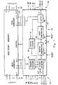
- the node 20 comprises a plurality of input ports 21 and a plurality of output ports 22.
- a multiport memory 23 is coupled between the input and output ports 21, 22.
- the memory 23 has a predetermined number of memory locations available for storage of data packets applied to each of the input ports 21.
- Control logic 24 is coupled to the input and output ports 21, 22 and the multiport memory 23 which controls the storage of data packets in the memory 23.
- the control logic 24 also controls the routing of the data packets to the output ports 22 in accordance with routing tag signals contained in the data packets.
- the transmission protocol for receiving data packets by way of the input ports 21 is executed by a plurality of receiving handshake signal lines 25 coupled to the control logic 24.
- the transmission protocol for sending data packets from the output ports 22 is executed by a plurality of sending handshake signal lines 26 also coupled to the control logic 24.
- the control logic 24 comprises tag status logic register 30 coupled to the input ports 21, the receive handshake signal lines 25, and the memory 23, which stores both the routing tag signals and status signals indicative of the full/ empty status of each of the memory locations in the memory 23.
- the control logic 24 also includes priority encoder logic 31 coupled to the input ports 21, the memory 23 and the tag status register logic 30.
- the priority encoder logic 31 is adapted to monitor the full/empty status of the memory locations, write the routing tag signals into registers of the status register 30 and write data packets corresponding to the routing tag signals into selected memory locations.
- the control logic 24 further comprises arbitration logic 32 coupled to the tag status register logic 30 and latch logic 36.
- the arbitration logic 32 is designed to examine routing tags stored in the status register logic 30 and resolve conflicting requests based upon a predetermined priority arbitration scheme. In the arbitration process, read addresses are generated and stored in the latch logic 36 that determine the output of data packets through the appropriate output port 22 such that they correspond to the routing tag signals selected by the arbitration logic 32.
- the arbitration logic 32 includes buffer arbitration logic 33 which is designed to arbitrate among routing tags entering the same input port 21 that contend for output from the same output port 22.
- the arbitration logic 32 randomly selects a particular routing tag therefrom.
- port arbitration logic 34 is coupled to the buffer arbitration logic 33 and to the latch logic 36 which is adapted to arbitrate among all routing tags transmitted by the buffer arbitration logic 33 which contend for the same output port 22 and selects one routing tag and its associated packet therefrom for output from that particular output port 22.
- Status update logic 35 is coupled to the latch logic 36 and the sending handshake signal lines 26.
- the status update logic 35 is designed to generate signals which reset the full/empty status of the registers corresponding to the data packets applied to and transmitted from any of the output ports 22.
- the present invention may be employed as an N x M switch node that accepts data packets at any of N input ports 21 and routes each to any of M output ports 22.
- the output port 22 selected is determined by the routing tag signal in the data packet.
- the control logic 24 is designed so that the data packets are effectively sorted according to their desired output port destination.
- the arbitration logic 32 randomly, in a statistical sense, chooses among data packets that are directed to the same output port 22.
- the algorithm implemented by the arbitration logic 32 is designed so that data packets will not wait indefinitely to be routed from the switch node 20.
- the control logic 24 performs handshaking with other switch nodes or processors, or the like, to which the node 20 is connected.
- the control logic 24 generates addresses into the memory 23 and arbitrates among data packets. All incoming requests to the switch node 20 are accompanied by the routing tag signals. These routing tag signals are a predetermined number of bits in the data packet. These bits, along with a full/empty status bit, are stored in the tag status register logic 30.
- the status register logic 30 contains N x P cells, where N is the number of input ports 21 and P is the number of storage locations allowed per input port 21. Each cell corresponds to a memory location and stores both the status and tag bits.
- the priority encoder logic 31 selects the first available cell allotted for a given input port 21 when a request is received. As long as the status bits are not all full, a "not full,” or grant signal is sent to the sending node or processor which is interpreted to mean proceed. The requesting packet is then written into its assigned location in the memory 23, the tag bits are written into the tag status register logic 30 and the corresponding full/empty bit is set to "full".
- Arbitration among packets takes place in two steps. First, all the tag bits in full cells are decoded and grouped according to the desired output port 22. Then the buffer arbitration logic 33 randomly chooses among packets that entered the same input port 21 that also are destined for the same output port 22. In the second step, the port arbitration logic 34 randomly chooses between any packets presented by the buffer arbitration logic 33 that are destined for the same output port 22. As long as data packets that entered the same input port 21 are destined for different output ports 22, all are allowed to participate in the second step of arbitration. Thus, none are blocked due to their position in the memory 23. A packet can only be blocked due to competition with another packet for the same output port 22.
- the results of the arbitration process are latched in the latch logic 36 and requests are generated for those output ports 22 desired by the data packets. Appropriate read addresses are generated for each output port 22 that is to be used. For those requests that are granted, the appropriate full/empty status bits are reset to "empty.” If any request is not granted, the packet remains in the memory 23 and repeats the arbitration process during the next cycle.
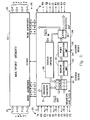
- Fig. 3 a top- level detailed block diagram of the control logic 24 which may be employed in the packet switching node of Fig. 2 is shown.
- Fig. 3 shows the interconnection of a plurality of logic blocks which incorporate the status update logic 35, tag status register logic 30, priority encoder logic 31, buffer arbitration logic 33, port arbitration logic 34 and latch logic 36 which comprise the various logic portions of the control logic 24 utilized in the present invention.
- the logic circuit shown in Fig. 3 is partitioned so that those portions of the tag status register logic 30, priority encoder logic 31 and buffer arbitration logic 33 associated with one input port 25 are grouped together to form four identical logic modules which comprise four input port logic sections 70a-d. Similarly, those portions of the port arbitration logic 34 and latch logic 36 associated with each output port 26 are grouped together to form four identical logic modules comprising four output port logic sections 71a-d.
- FIG. 3 Detailed schematics of the various logic portions shown in Fig. 3 are illustrated in Figs. 4 through 11 hereinbelow. There is a one to one correspondance between the signal line identifiers in Fig. 3 and the signal line identifiers used in the Figs. 4 through 11. The balance of the Figures will not be discussed in explicit detail except to the extent necessary to explain their operation and function in the overall switch node 20.
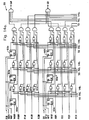
- Fig. 4 shows the detailed logic design of one input port section 70.
- the status register logic 30 comprises nine flip-flops 72a-i which are coupled to tag decoders or demultiplexers 73a-c and the priority encoder logic 31 which employs a plurality of nand gates 78a-c.
- Decoded tag signals are coupled from the demultiplexers 73 to the buffer arbitration logic 33 which comprises buffer arbitration logic circuits 74a-d.
- Intermediate status register logic comprising registers 75a-h is used to ensure correct timing of the signals.
- a modulo 3 counter 76 is employed to determine the current priority used by the buffer arbitration logic circuits 74a-d and is enabled by counter enable logic 77.
- the priority encoder logic 31 is coupled through the intermediate status register 75f-h to tag status register logic clock enable logic 79. Full/ empty flip-flops 72g-i utilized in the tag status register logic 30 are cleared by status reset logic 80.
- the logic circuit of Fig. 4 operates as follows.
- the input port logic section 70a shown in Fig. 4 stores a 2 bit tag and its associated request signal into one of the three locations in the tag status register logic 30 comprising flip-flops 72a-i.
- the particular storage location is determined by the priority encoder logic 31 comprising nand gates 78 and the clock enable logic 79.
- the priority encoder logic 31 produces a 2 bit address indicating the first available location and a signal to indicate if there are none. These three signals are also provided to the multiport memory 23 and form the write address for the corresponding input port 21.
- the tags that have been stored in the tag status register logic 30 are each decoded by the demultiplexers 73. At most, one signal output from each demultiplexer 73 will be active and will correspond to the desired output port 22.
- the signal wires from the demultiplexers 73 are physically grouped by corrresponding output port 22 and are input to four buffer arbitration logic circuits 74, comprising the buffer arbitration logic 33, with each circuit being associated with a different output port 22.
- the priority used by each buffer arbitration logic circuit 74 is provided by a modulo 3 counter 76.
- Each buffer arbitration logic circuit 74 outputs a two bit address of the selected tag and corresponding packet, along with a signal that indicates if any tag desires that output port 22.
- the modulo 3 counter 76 is incremented, and hence the priority changes, according to a signal derived from counter enable logic 77.
- the modulo 3 counter 76 is enabled only if the location with highest priority is empty, as indicated by the tag status register logic full/empty flip-flops 72g-i, or if a clear signal is produced by the status update logic 35 indicating that the packet in the location with highest priority has been transmitted.
- the clear signals from the status update logic 35 are combined with a master reset signal and a clock signal in status reset logic 80.
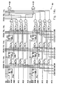
- FIG. 5 there is shown the detailed logic design of an output port logic section 71.
- the four to one address multiplexers 93a-b and gates 90 which comprise the port arbitration logic 34 are coupled to the latch logic 36 comprising flip-flops 94a-h.
- the output of the port arbitration logic 34 is also directly coupled to the address multiplexers 93a-b.
- a modulo 4 counter 91 is coupled to the port arbitration logic 34 and determines the current priority.
- Counter enable logic 92 controls whether or not the modulo 4 counter 91 is incremented.
- each output port logic section 71 receives one address and request signal from each input port logic section 70, as shown in Fig. 3.
- the request signals are processed by the port arbitration logic 34 according to the priority indicated by the modulo 4 counter 91.
- the 2 bit address of the selected input port 21 is output to the latch logic 36 along with a request signal indicating if there is any request.
- This 2 bit input port address also allows the 4 to 1 address multiplexers 93 to select the corresponding 2 bit status register address from the selected input port 21 which is also output to the latch logic 36.
- the 4 bits of address form a read address which is coupled to the corresponding output port 22 in the multiport memory 23 to access the packet associated with the selected tag bits.
- the modulo four counter 91 is incremented, changing the priority used by the port arbitration logic 34, according to signals from the counter enable logic 92.
- the counter enable logic 92 produces an increment signal whenever the input port 21 with highest priority has no request for the associated output port 22 or it has a request which is honored and the packet is transmitted. As long as the FULLI signal is TRUE, indicating that an output device or switch node attached to the associated output port 22 is "not full,” the selected request will be sent. Otherwise the request must wait until the output device is no longer full.
- each read address decoder 97 enables a single signal, which corresponds to one of 12 status flip-flops in the tag status register logic 30 if there is a request associated with the read address at the input and the "not full" signal is true.
- the clear signals from all the read address decoders 97 are merged into a single set of signals which are connected to the status reset logic 80 and the counter enable logic 77 in Fig. 4. There are at most four clear signals active at one time.
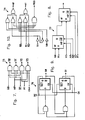
- a design of the demultiplexer 73 used in the input port logic 70 of Fig. 4 is shown.
- Fig. 8 shows a design of the three to one multiplexer 77 used in the input port logic 70 of Fig. 4.
- Fig. 9 shows a design of the modulo 3 counter 76 used in the input port logic 70 of Fig. 4.
- Fig. 10 shows a design of the 3 input arbitration logic 74 used in the input port logic 70 of Fig. 4.
- Fig. 11 shows a design of a four-to-twelve demultiplexer circuit 97 for use in the status update logic 35 of Fig. 6.
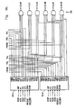
- the memory 23 is comprised of write address select decode logic 40 and read address row and column select decode logic 41 which are coupled to a 12 x 4 x 3 bit array 42.
- the multiport memory 23 is designed to accept up to four write addresses and 12 bits which comprise a data packet associated with each write address at an input port 21 and up to four read addresses and produce the four corresponding 12 bit data packets at an output port 22 during each clock cycle.
- Each write address is decoded in the write address logic 40 so that one of three memory cell select lines is enabled.
- Each read address is decoded in the read address logic 41 so that one of four row select and one of three column select lines is enabled.
- the memory cell at the intersection of the row and column select lines presents its contents at the corresponding output port 22.
- Detailed schematics of the various logic blocks shown in Fig. 12 are shown in Figs. 13 through 18 hereinbelow.
- Fig. 13 shows the organization of the 12 x 4 x 3 bit array 42. It is comprised of twelve identical copies of a 4 x 3 bit memory array 50. The write, row, and column select lines are all connected to each 4 x 3 bit memory array 50.
- Fig. 14 shows the detailed logic design of the 4 x 3 memory array 50.
- Flip-flops 60a-I are used to store one bit of information each.
- Each input port 21 has an exclusive set of three memory locations into which it can write, which corresponds to three flip-flops that are in the same row, represented by 60a-c, 60d-f, etc.
- Fig. 15 shows the detailed design of the write address select decode logic 40 which is comprised of four identical 2 to 3 demultiplexers 51.
- the detailed logic design of the 2 to 3 demultiplexer 51 is shown in Fig. 16.
- Fig. 17 shows the detailed design of the read address row and column select decode logic 41 which is comprised of four identical row and column decoders 52.
- the detailed logic design of a row and column decoder 52 is shown in Fig. 18.
- Fig. 19 shows a timing diagram for the multiport memory packet switching node 20 of Fig. 2.
- the system clock which is externally generated, is comprised of two non-overlapping phases, ⁇ 1 and ⁇ 2.
- the rising edge of ⁇ 1 initiates the generation of all read and write addresses. Any data packet and its corresponding tag and request signal must be stable prior to the rising edge of q)2. Upon the rising edge of q)2, new data packets are written into the multiport memory 23 and the tag status register logic 30 is updated. Conflicts among tags are resolved at this time. The buffer and port priorities are also changed if enabled at this time.
- the packet switching node employs a multiport memory to store and sort data packets based upon the output port destinations thereof.
- the packet switching node eliminates the problem of contention between data packets arriving at an input port of the node whose destinations are different output ports.
- the present invention also provides for a packet switching node which has improved performance and higher throughput.
Landscapes
- Engineering & Computer Science (AREA)
- Theoretical Computer Science (AREA)
- Physics & Mathematics (AREA)
- Computer Hardware Design (AREA)
- Signal Processing (AREA)
- Computer Networks & Wireless Communication (AREA)
- General Engineering & Computer Science (AREA)
- General Physics & Mathematics (AREA)
- Software Systems (AREA)
- Mathematical Physics (AREA)
- Data Exchanges In Wide-Area Networks (AREA)
- Use Of Switch Circuits For Exchanges And Methods Of Control Of Multiplex Exchanges (AREA)
- Multi Processors (AREA)
Claims (2)
Applications Claiming Priority (2)
| Application Number | Priority Date | Filing Date | Title |
|---|---|---|---|
| US06/661,996 US4630258A (en) | 1984-10-18 | 1984-10-18 | Packet switched multiport memory NXM switch node and processing method |
| US661996 | 1984-10-18 |
Publications (2)
| Publication Number | Publication Date |
|---|---|
| EP0198010A1 EP0198010A1 (de) | 1986-10-22 |
| EP0198010B1 true EP0198010B1 (de) | 1990-03-21 |
Family
ID=24655970
Family Applications (1)
| Application Number | Title | Priority Date | Filing Date |
|---|---|---|---|
| EP85905143A Expired - Lifetime EP0198010B1 (de) | 1984-10-18 | 1985-09-26 | Mxm-multiport-speicherknotenstelle und verarbeitungsverfahren zur paketvermittlung |
Country Status (8)
| Country | Link |
|---|---|
| US (1) | US4630258A (de) |
| EP (1) | EP0198010B1 (de) |
| JP (1) | JPH0638607B2 (de) |
| KR (1) | KR900006791B1 (de) |
| DE (1) | DE3576775D1 (de) |
| IL (1) | IL76532A0 (de) |
| SG (1) | SG38090G (de) |
| WO (1) | WO1986002512A1 (de) |
Families Citing this family (53)
| Publication number | Priority date | Publication date | Assignee | Title |
|---|---|---|---|---|
| US4837676A (en) * | 1984-11-05 | 1989-06-06 | Hughes Aircraft Company | MIMD instruction flow computer architecture |
| US4696000A (en) * | 1985-12-12 | 1987-09-22 | American Telephone And Telegraph Company, At&T Bell Laboratories | Nonblocking self-routing packet and circuit switching network |
| BE904100A (fr) * | 1986-01-24 | 1986-07-24 | Itt Ind Belgium | Systeme de commutation. |
| US4748618A (en) * | 1986-05-21 | 1988-05-31 | Bell Communications Research, Inc. | Telecommunications interface |
| US4754451A (en) * | 1986-08-06 | 1988-06-28 | American Telephone And Telegraph Company, At&T Bell Laboratories | N-by-N "knockout" switch for a high-performance packet switching system with variable length packets |
| JPH08214008A (ja) * | 1987-02-06 | 1996-08-20 | Fujitsu Ltd | 自己ルーチングスイッチ |
| US4763122A (en) * | 1987-03-18 | 1988-08-09 | International Business Machines Corporation | Parallel switching with round robin priority |
| US4831616A (en) * | 1987-03-31 | 1989-05-16 | Huber David R | Multiplexed fiber optics wideband data distribution system |
| US4910731A (en) * | 1987-07-15 | 1990-03-20 | Hitachi, Ltd. | Switching system and method of construction thereof |
| US6330240B1 (en) | 1987-04-24 | 2001-12-11 | Hitachi, Ltd. | ATM cell switching system |
| US5365519A (en) | 1991-03-05 | 1994-11-15 | Hitachi, Ltd. | ATM switch1ng system connectable to I/O links having different transmission rates |
| US5117420A (en) * | 1987-04-27 | 1992-05-26 | Thinking Machines Corporation | Method and apparatus for routing message packets |
| US4984235A (en) * | 1987-04-27 | 1991-01-08 | Thinking Machines Corporation | Method and apparatus for routing message packets and recording the roofing sequence |
| USRE36751E (en) * | 1987-07-15 | 2000-06-27 | Hitachi, Ltd. | ATM switching system connectable to I/O links having different transmission rates |
| US5136718A (en) * | 1987-09-04 | 1992-08-04 | Digital Equipment Corporation | Communications arrangement for digital data processing system employing heterogeneous multiple processing nodes |
| US5367688A (en) * | 1987-09-04 | 1994-11-22 | Digital Equipment Corporation | Boot system for distributed digital data processing system |
| US4845722A (en) * | 1987-10-16 | 1989-07-04 | Digital Equipment Corporation | Computer interconnect coupler employing crossbar switching |
| US4887076A (en) * | 1987-10-16 | 1989-12-12 | Digital Equipment Corporation | Computer interconnect coupler for clusters of data processing devices |
| US4885739A (en) * | 1987-11-13 | 1989-12-05 | Dsc Communications Corporation | Interprocessor switching network |
| JP2667868B2 (ja) * | 1988-04-06 | 1997-10-27 | 株式会社日立製作所 | セル・スイッチング・システム |
| US5233603A (en) * | 1988-04-21 | 1993-08-03 | Nec Corporation | Packet switch suitable for integrated circuit implementation |
| US4891803A (en) * | 1988-11-07 | 1990-01-02 | American Telephone And Telegraph Company | Packet switching network |
| US5046000A (en) * | 1989-01-27 | 1991-09-03 | International Business Machines Corporation | Single-FIFO high speed combining switch |
| US5249292A (en) * | 1989-03-31 | 1993-09-28 | Chiappa J Noel | Data packet switch using a primary processing unit to designate one of a plurality of data stream control circuits to selectively handle the header processing of incoming packets in one data packet stream |
| DE4004956A1 (de) * | 1990-02-19 | 1991-08-22 | Philips Patentverwaltung | Koppelelement fuer ein asynchrones zeitvielfachuebermittlungssystem |
| EP0521027A4 (en) * | 1990-03-22 | 1994-10-19 | Australian & Overseas Telecom | Multicasting method for a telecommunications network |
| US5265257A (en) * | 1990-06-22 | 1993-11-23 | Digital Equipment Corporation | Fast arbiter having easy scaling for large numbers of requesters, large numbers of resource types with multiple instances of each type, and selectable queuing disciplines |
| JP2770936B2 (ja) * | 1990-12-18 | 1998-07-02 | インターナショナル・ビジネス・マシーンズ・コーポレイション | 通信ネットワークおよび通信チャンネルをつくる方法 |
| US5825773A (en) * | 1991-03-20 | 1998-10-20 | Hitachi, Ltd. | Switching system for transferring broadcast packet held in broadcast buffer received from input port to output ports according to the state of each output port |
| US5321813A (en) * | 1991-05-01 | 1994-06-14 | Teradata Corporation | Reconfigurable, fault tolerant, multistage interconnect network and protocol |
| JP3679813B2 (ja) * | 1991-07-22 | 2005-08-03 | 株式会社日立製作所 | 並列計算機 |
| SE515148C2 (sv) * | 1993-06-23 | 2001-06-18 | Ericsson Telefon Ab L M | Styrning av cellväljare |
| DE4343588A1 (de) * | 1993-12-21 | 1995-06-22 | Sel Alcatel Ag | Verfahren und Einrichtung zur zufälligen Auswahl einer von N gleichen Einheiten, sowie Koppelelement, Koppelnetz und Vermittlungsstelle damit |
| WO1996007139A1 (en) * | 1994-09-01 | 1996-03-07 | Mcalpine Gary L | A multi-port memory system including read and write buffer interfaces |
| JP3269273B2 (ja) * | 1994-09-02 | 2002-03-25 | 三菱電機株式会社 | セル交換装置及びセル交換システム |
| US5566171A (en) * | 1995-03-15 | 1996-10-15 | Finisar Corporation | Multi-mode high speed network switch for node-to-node communication |
| GB2300088B (en) * | 1995-04-19 | 1999-06-16 | Northern Telecom Ltd | Telecommunications switches |
| US6185222B1 (en) * | 1995-09-28 | 2001-02-06 | Cisco Technology, Inc. | Asymmetric switch architecture for use in a network switch node |
| SE520465C2 (sv) * | 1997-07-11 | 2003-07-15 | Ericsson Telefon Ab L M | Redundansterminering i flerstegsväxel för ATM-trafik |
| US6301637B1 (en) * | 1998-06-08 | 2001-10-09 | Storage Technology Corporation | High performance data paths |
| US6611895B1 (en) * | 1998-06-08 | 2003-08-26 | Nicholas J. Krull | High bandwidth cache system |
| US6563818B1 (en) * | 1999-05-20 | 2003-05-13 | Advanced Micro Devices, Inc. | Weighted round robin cell architecture |
| US6519697B1 (en) | 1999-11-15 | 2003-02-11 | Ncr Corporation | Method and apparatus for coordinating the configuration of massively parallel systems |
| US6418526B1 (en) | 1999-11-15 | 2002-07-09 | Ncr Corporation | Method and apparatus for synchronizing nodes in massively parallel systems |
| US6745240B1 (en) | 1999-11-15 | 2004-06-01 | Ncr Corporation | Method and apparatus for configuring massively parallel systems |
| US6412002B1 (en) | 1999-11-15 | 2002-06-25 | Ncr Corporation | Method and apparatus for selecting nodes in configuring massively parallel systems |
| US6717951B2 (en) * | 1999-12-29 | 2004-04-06 | Intel Corporation | Method and apparatus for determining priority of network packets |
| CN1366402B (zh) * | 2002-02-05 | 2010-10-13 | 威盛电子股份有限公司 | 分组交换的负载平衡装置 |
| DE10212374B4 (de) * | 2002-03-20 | 2005-12-08 | Siemens Ag | Lastverteilung auf periphere Einrichtungen eines paketbasierten Vermittlungssystems |
| US20050166252A1 (en) * | 2004-01-06 | 2005-07-28 | Sharp Laboratories Of America, Inc. | Personal video recorder |
| US20140050221A1 (en) * | 2012-08-16 | 2014-02-20 | Stmicroelectronics, Inc. | Interconnect arrangement |
| CN112383474B (zh) * | 2020-10-15 | 2022-11-01 | 中国科学院国家空间科学中心 | 一种多端口的SpaceFibre路由IP |
| CN114826930B (zh) * | 2022-04-20 | 2024-02-23 | 山东云海国创云计算装备产业创新中心有限公司 | 一种实现扁平式蝴蝶型网络拓扑的系统及方法 |
Family Cites Families (24)
| Publication number | Priority date | Publication date | Assignee | Title |
|---|---|---|---|---|
| US3629846A (en) * | 1970-06-11 | 1971-12-21 | Bell Telephone Labor Inc | Time-versus-location pathfinder for a time division switch |
| US4149240A (en) * | 1974-03-29 | 1979-04-10 | Massachusetts Institute Of Technology | Data processing apparatus for highly parallel execution of data structure operations |
| US4153932A (en) * | 1974-03-29 | 1979-05-08 | Massachusetts Institute Of Technology | Data processing apparatus for highly parallel execution of stored programs |
| US3962706A (en) * | 1974-03-29 | 1976-06-08 | Massachusetts Institute Of Technology | Data processing apparatus for highly parallel execution of stored programs |
| US4145733A (en) * | 1974-03-29 | 1979-03-20 | Massachusetts Institute Of Technology | Data processing apparatus for highly parallel execution of stored programs |
| FR2305907A1 (fr) * | 1975-03-27 | 1976-10-22 | Materiel Telephonique | Dispositif de controle destine a un reseau de commutation pour voies multiplexees dans le temps |
| US3979733A (en) * | 1975-05-09 | 1976-09-07 | Bell Telephone Laboratories, Incorporated | Digital data communications system packet switch |
| US4074233A (en) * | 1976-06-30 | 1978-02-14 | Norlin Music, Inc. | Selection switch memory circuit |
| US4130885A (en) * | 1976-08-19 | 1978-12-19 | Massachusetts Institute Of Technology | Packet memory system for processing many independent memory transactions concurrently |
| US4128882A (en) * | 1976-08-19 | 1978-12-05 | Massachusetts Institute Of Technology | Packet memory system with hierarchical structure |
| US4201890A (en) * | 1978-03-17 | 1980-05-06 | International Telephone And Telegraph | Multiport digital switching element |
| US4229790A (en) * | 1978-10-16 | 1980-10-21 | Denelcor, Inc. | Concurrent task and instruction processor and method |
| FR2447652A1 (fr) * | 1979-01-24 | 1980-08-22 | Materiel Telephonique | Operateur pour reseau de commutation de donnees numeriques par paquets |
| FR2458196A1 (fr) * | 1979-06-01 | 1980-12-26 | Materiel Telephonique | Niveau de commutation d'un operateur pour reseau de commutation de donnees numeriques par paquets |
| US4365292A (en) * | 1979-11-26 | 1982-12-21 | Burroughs Corporation | Array processor architecture connection network |
| US4314233A (en) * | 1979-12-18 | 1982-02-02 | Burroughs Corporation | Four-wire speed independent arbiter switch for digital communication networks |
| US4450554A (en) * | 1981-08-10 | 1984-05-22 | International Telephone And Telegraph Corporation | Asynchronous integrated voice and data communication system |
| JPS5857940A (ja) * | 1981-10-03 | 1983-04-06 | 松下電工株式会社 | 積層板 |
| JPS58150349A (ja) * | 1982-03-02 | 1983-09-07 | Mitsubishi Electric Corp | パケツト通信ネツトワ−ク |
| US4482996A (en) * | 1982-09-02 | 1984-11-13 | Burroughs Corporation | Five port module as a node in an asynchronous speed independent network of concurrent processors |
| FR2538976A1 (fr) * | 1982-12-29 | 1984-07-06 | Servel Michel | Systeme de commutation de paquets synchrones de longueur fixe |
| JPS59135953A (ja) * | 1983-01-26 | 1984-08-04 | Fujitsu Ltd | デ−タ送出経路決定方式 |
| FR2549673B1 (fr) * | 1983-07-19 | 1989-06-30 | Thomson Csf Mat Tel | Commutateur elementaire pour autocommutateur utilisant une technique de multiplexage asynchrone |
| JP5857940B2 (ja) | 2012-10-31 | 2016-02-10 | 株式会社デンソー | 無線通信機 |
-
1984
- 1984-10-18 US US06/661,996 patent/US4630258A/en not_active Expired - Lifetime
-
1985
- 1985-09-26 WO PCT/US1985/001840 patent/WO1986002512A1/en not_active Ceased
- 1985-09-26 DE DE8585905143T patent/DE3576775D1/de not_active Expired - Fee Related
- 1985-09-26 KR KR1019860700369A patent/KR900006791B1/ko not_active Expired
- 1985-09-26 JP JP50450585A patent/JPH0638607B2/ja not_active Expired - Lifetime
- 1985-09-26 EP EP85905143A patent/EP0198010B1/de not_active Expired - Lifetime
- 1985-09-29 IL IL76532A patent/IL76532A0/xx not_active IP Right Cessation
-
1990
- 1990-05-31 SG SG380/90A patent/SG38090G/en unknown
Also Published As
| Publication number | Publication date |
|---|---|
| DE3576775D1 (de) | 1990-04-26 |
| KR880700566A (ko) | 1988-03-15 |
| JPH0638607B2 (ja) | 1994-05-18 |
| EP0198010A1 (de) | 1986-10-22 |
| IL76532A0 (en) | 1986-01-31 |
| SG38090G (en) | 1990-08-03 |
| KR900006791B1 (ko) | 1990-09-21 |
| WO1986002512A1 (en) | 1986-04-24 |
| US4630258A (en) | 1986-12-16 |
| JPS62500902A (ja) | 1987-04-09 |
Similar Documents
| Publication | Publication Date | Title |
|---|---|---|
| US4630258A (en) | Packet switched multiport memory NXM switch node and processing method | |
| EP0200780B1 (de) | Paketvermittlungsknoten mit mehreren warteschlangen und steuerungsverfahren | |
| Tamir et al. | Dynamically-allocated multi-queue buffers for VLSI communication switches | |
| EP0197103B1 (de) | Belastungsausgleich für paketvermittlungsknoten | |
| Tamir et al. | High-performance multi-queue buffers for VLSI communications switches | |
| EP0195589B1 (de) | Vermittlungssystem für Datenübertragung | |
| US6314487B1 (en) | Adaptive routing controller of a crossbar core module used in a crossbar routing switch | |
| Tamir et al. | Symmetric crossbar arbiters for VLSI communication switches | |
| US7940666B2 (en) | Communication node architecture in a globally asynchronous network on chip system | |
| US5218676A (en) | Dynamic routing system for a multinode communications network | |
| EP0334954B1 (de) | Geschichtetes netz | |
| US4952930A (en) | Multipath hierarchical network | |
| EP0744851A1 (de) | Verteiltes Datenverarbeitungssystem | |
| JPH02263260A (ja) | メモリアクセススイッチネットワーク | |
| EP0405208B1 (de) | Mehrstufiges Netz mit verteilter Steuerung | |
| US5371893A (en) | Look-ahead priority arbitration system and method | |
| IE49451B1 (en) | Digital communication networks employing speed independent switches | |
| EP0018756A2 (de) | Geschwindigkeitsunabhängiger Entscheidungsschalter für digitale Übertragungsnetzwerke | |
| JPH05241947A (ja) | 分散クロスバー・スイッチ・アーキテクチャにおける交換接続の配列。 | |
| EP1360595A2 (de) | Skalierbare verbindungsstruktur für parallelverarbeitung und paralellspeicherzugriff | |
| JP3031591B2 (ja) | アクセス調停方式 | |
| JP2976700B2 (ja) | プロセッサ間同期制御方式 | |
| JP3609908B2 (ja) | 計算機接続装置 | |
| JPH04291548A (ja) | 高速大容量マトリクス型時間分割ラベル交換方式 | |
| Daniel et al. | A router architecture for flexible routing and switching in multihop point-to-point networks |
Legal Events
| Date | Code | Title | Description |
|---|---|---|---|
| PUAI | Public reference made under article 153(3) epc to a published international application that has entered the european phase |
Free format text: ORIGINAL CODE: 0009012 |
|
| 17P | Request for examination filed |
Effective date: 19860612 |
|
| AK | Designated contracting states |
Kind code of ref document: A1 Designated state(s): DE FR GB IT NL |
|
| 17Q | First examination report despatched |
Effective date: 19880411 |
|
| RAP1 | Party data changed (applicant data changed or rights of an application transferred) |
Owner name: HUGHES AIRCRAFT COMPANY |
|
| GRAA | (expected) grant |
Free format text: ORIGINAL CODE: 0009210 |
|
| AK | Designated contracting states |
Kind code of ref document: B1 Designated state(s): DE FR GB IT NL |
|
| ET | Fr: translation filed | ||
| REF | Corresponds to: |
Ref document number: 3576775 Country of ref document: DE Date of ref document: 19900426 |
|
| ITF | It: translation for a ep patent filed | ||
| PLBE | No opposition filed within time limit |
Free format text: ORIGINAL CODE: 0009261 |
|
| STAA | Information on the status of an ep patent application or granted ep patent |
Free format text: STATUS: NO OPPOSITION FILED WITHIN TIME LIMIT |
|
| 26N | No opposition filed | ||
| ITTA | It: last paid annual fee | ||
| PGFP | Annual fee paid to national office [announced via postgrant information from national office to epo] |
Ref country code: FR Payment date: 19940808 Year of fee payment: 10 |
|
| PGFP | Annual fee paid to national office [announced via postgrant information from national office to epo] |
Ref country code: GB Payment date: 19940815 Year of fee payment: 10 |
|
| PGFP | Annual fee paid to national office [announced via postgrant information from national office to epo] |
Ref country code: DE Payment date: 19940824 Year of fee payment: 10 |
|
| PGFP | Annual fee paid to national office [announced via postgrant information from national office to epo] |
Ref country code: NL Payment date: 19940930 Year of fee payment: 10 |
|
| PG25 | Lapsed in a contracting state [announced via postgrant information from national office to epo] |
Ref country code: GB Effective date: 19950926 |
|
| PG25 | Lapsed in a contracting state [announced via postgrant information from national office to epo] |
Ref country code: NL Effective date: 19960401 |
|
| GBPC | Gb: european patent ceased through non-payment of renewal fee |
Effective date: 19950926 |
|
| PG25 | Lapsed in a contracting state [announced via postgrant information from national office to epo] |
Ref country code: FR Effective date: 19960531 |
|
| PG25 | Lapsed in a contracting state [announced via postgrant information from national office to epo] |
Ref country code: DE Effective date: 19960601 |
|
| NLV4 | Nl: lapsed or anulled due to non-payment of the annual fee |
Effective date: 19960401 |
|
| REG | Reference to a national code |
Ref country code: FR Ref legal event code: ST |