EP0200270A1 - Ladungsgekoppelte Anordnung und diese Anordnung umfassende Kamera - Google Patents
Ladungsgekoppelte Anordnung und diese Anordnung umfassende Kamera Download PDFInfo
- Publication number
- EP0200270A1 EP0200270A1 EP86200710A EP86200710A EP0200270A1 EP 0200270 A1 EP0200270 A1 EP 0200270A1 EP 86200710 A EP86200710 A EP 86200710A EP 86200710 A EP86200710 A EP 86200710A EP 0200270 A1 EP0200270 A1 EP 0200270A1
- Authority
- EP
- European Patent Office
- Prior art keywords
- charge
- section
- storage section
- electrode
- clock
- Prior art date
- Legal status (The legal status is an assumption and is not a legal conclusion. Google has not performed a legal analysis and makes no representation as to the accuracy of the status listed.)
- Granted
Links
- 238000005036 potential barrier Methods 0.000 claims description 8
- 230000027311 M phase Effects 0.000 claims description 6
- 230000005855 radiation Effects 0.000 claims description 5
- 238000001514 detection method Methods 0.000 claims description 4
- 239000004065 semiconductor Substances 0.000 claims description 4
- 230000001939 inductive effect Effects 0.000 claims description 2
- 238000010586 diagram Methods 0.000 description 14
- 230000010354 integration Effects 0.000 description 9
- 238000009826 distribution Methods 0.000 description 7
- 230000001419 dependent effect Effects 0.000 description 4
- XUIMIQQOPSSXEZ-UHFFFAOYSA-N Silicon Chemical compound [Si] XUIMIQQOPSSXEZ-UHFFFAOYSA-N 0.000 description 2
- 230000004888 barrier function Effects 0.000 description 2
- 230000006835 compression Effects 0.000 description 2
- 238000007906 compression Methods 0.000 description 2
- 238000006073 displacement reaction Methods 0.000 description 2
- 238000000605 extraction Methods 0.000 description 2
- 239000011159 matrix material Substances 0.000 description 2
- 229910052710 silicon Inorganic materials 0.000 description 2
- 239000010703 silicon Substances 0.000 description 2
- 239000000758 substrate Substances 0.000 description 2
- VYPSYNLAJGMNEJ-UHFFFAOYSA-N Silicium dioxide Chemical compound O=[Si]=O VYPSYNLAJGMNEJ-UHFFFAOYSA-N 0.000 description 1
- 238000010521 absorption reaction Methods 0.000 description 1
- 239000002800 charge carrier Substances 0.000 description 1
- 239000004020 conductor Substances 0.000 description 1
- 230000007423 decrease Effects 0.000 description 1
- 230000000694 effects Effects 0.000 description 1
- 238000012986 modification Methods 0.000 description 1
- 230000004048 modification Effects 0.000 description 1
- 230000035515 penetration Effects 0.000 description 1
- 230000002093 peripheral effect Effects 0.000 description 1
- 229910021420 polycrystalline silicon Inorganic materials 0.000 description 1
- 229910052814 silicon oxide Inorganic materials 0.000 description 1
Images




Classifications
-
- G—PHYSICS
- G11—INFORMATION STORAGE
- G11C—STATIC STORES
- G11C27/00—Electric analogue stores, e.g. for storing instantaneous values
- G11C27/04—Shift registers
-
- H—ELECTRICITY
- H04—ELECTRIC COMMUNICATION TECHNIQUE
- H04N—PICTORIAL COMMUNICATION, e.g. TELEVISION
- H04N25/00—Circuitry of solid-state image sensors [SSIS]; Control thereof
-
- H—ELECTRICITY
- H04—ELECTRIC COMMUNICATION TECHNIQUE
- H04N—PICTORIAL COMMUNICATION, e.g. TELEVISION
- H04N25/00—Circuitry of solid-state image sensors [SSIS]; Control thereof
- H04N25/70—SSIS architectures; Circuits associated therewith
- H04N25/71—Charge-coupled device [CCD] sensors; Charge-transfer registers specially adapted for CCD sensors
- H04N25/72—Charge-coupled device [CCD] sensors; Charge-transfer registers specially adapted for CCD sensors using frame transfer [FT]
-
- H—ELECTRICITY
- H04—ELECTRIC COMMUNICATION TECHNIQUE
- H04N—PICTORIAL COMMUNICATION, e.g. TELEVISION
- H04N25/00—Circuitry of solid-state image sensors [SSIS]; Control thereof
- H04N25/70—SSIS architectures; Circuits associated therewith
- H04N25/71—Charge-coupled device [CCD] sensors; Charge-transfer registers specially adapted for CCD sensors
- H04N25/745—Circuitry for generating timing or clock signals
-
- H—ELECTRICITY
- H10—SEMICONDUCTOR DEVICES; ELECTRIC SOLID-STATE DEVICES NOT OTHERWISE PROVIDED FOR
- H10F—INORGANIC SEMICONDUCTOR DEVICES SENSITIVE TO INFRARED RADIATION, LIGHT, ELECTROMAGNETIC RADIATION OF SHORTER WAVELENGTH OR CORPUSCULAR RADIATION
- H10F39/00—Integrated devices, or assemblies of multiple devices, comprising at least one element covered by group H10F30/00, e.g. radiation detectors comprising photodiode arrays
- H10F39/10—Integrated devices
- H10F39/12—Image sensors
- H10F39/15—Charge-coupled device [CCD] image sensors
- H10F39/153—Two-dimensional or three-dimensional array CCD image sensors
Definitions
- the invention relates to a charge-coupled device comprising:
- the invention further relates to a camera provided with such a device.
- Such a charge-coupled device is distinguished from the conventional charge-coupled devices in that the information is stored with a higher density in the channel than it is transported therein. As will appear hereinafter, this property is of importance more particularly, though not exclusively, for image sensors.
- image sensors of, for example, the frame transfer type, in which the CCD acts as a sensor, as a transport channel and as a memory it is usual, for example, in the case of 4-phase transport to operate the sensor section also as a 4-phasec-system.
- a photosensitive element or pixel then corresponds to four electrodes.
- one storage site also corresponds to four electrodes.
- this means for the photo- sensitive section a doubling of the number of pixels per unit surface area.
- the frame of the charge packets is extended by first shifting only the charge packet closest to the output over a certain distance, and by then shifting this packet and simultaneously the next packet etc., in which event each time the distances between successive charge packets are made sufficiently large for the normal 4-phase transport.
- the inverse is the case in the storage section, in which the frame is compressed again, as a result of which the charge packets are stored again in every second electrode. Because of the resemblance to the extraction and compression of the bellows of an accordion, this device is designated as the "accordion sensor" in the lecture entitled "The Accodion Imager: an Ultra-High Density Frame Transfer CCD" by A.J.P. Theu Giveaway et al on the International Electron Device Meeting 1984 (San Francisco 1984), Digest, pages 40/43.
- a charge-coupled image sensor also comprises electronic control means indicating how and when the device is expected to operate.
- These electronic means indicate by way of example when an integration period begins and ends, when a frame of the photosensitive section has to be shifted into the storage section, when the frame has been shifted completely into the storage section, and so on.
- These electronic means essentially comprise a number of counters which count the pulses of a clock and give up a signal after a given number of pulses, as a result of which the device can pass from one condition to another.
- An additional complication may then occur due to the "interlacing"mode of operation, in which the pixels ln two successive frames are relatively shifted by a half vertical pitch. In this mode of operation, the numbers of clock pulses required for the transport of the two frames are generally not equal to each other. Due to the complexity, these electronic control means have mostly to be arranged externally, that is to say outside the chip of the sensor itself.
- the invention has for its object inter alia to considerably simplify these electronic control means for CCD's of the accordion type described above and/or to shape them into such a form that, if desired, they may be in- teg-rated at least in part with the charge-coupled device.
- the invention is based inter alia on the recognition of the fact that in a CCD of the accordion type the potential distribution over the clock electrodes at a given instant t (or a parameter corresponding unambiguously to this potential distribution) is indicative of the condition of the charge-coupled device.
- the invention is further based on the recognition of the fact that by detection of the potential distribution it is possible to determine the instant t at which a next operation has to be started.
- a charge-coupled device is characteri.zed in that second means are provided by which the condition of the charge-coupled device can be detected and, depending upon this condition, an adjustment signal can be generated, which is used as a control signal for causing the charge-coupled device to pass to a next condition.
- Fig. 1 shows a diagrammatic plan view of an accordion CCD sensor of the FT type, as described inter alia in the aforementioned publication of Theu Giveaway et al.
- the arrangement comprises a large number of vertically represented charge-coupled devices 2, of which only five are shown in Fig. 1.
- the lateral boundaries 3 of the CCD's are indicated by broken lines.
- the arrows 4 in the channels 2 indicate the charge transport direction.
- the mat of charge-coupled devices 2 is subdivided into two sections, i.e. the A section, by means of which a projected radiation image is converted into a pattern.- of charge packets, and a B-section, which forms a memory in which the pattern generated in A can be stored for reading.
- the matrix is read by means of the horizontal C register, in which each time one line of the matrix can be transported in the usual charge-coupled manner to the left and can be read one by one at the output of the detector 5.
- the arrangement further comprises a system of clock electrodes which for the sake of simplicity are indicated by lines 6 in the diagrammatic plan view of Fig. 1.
- the clock voltages required for the charge transport are applied by means of the shift register 7 for the A section and the shift registers 8 for the B section. These shift registers will be described more fully hereinafter.
- the C register is assumed to be operated in a usual 2-, 3- or 4-phase manner, which will not be described further.
- Fig. 2 The lefthand part of Fig. 2 is a sectional view transverse to the charge transport direction of a section comprising five charge-coupled devices 2.
- the arrangement is manufactured by way of example in an n-type silicon body 10 having a p-type surface region 11 (p-well) adjoining the surface 12.
- the p-type layer or zone 11 is provided with the channels of the charge-coupled devices 2 in the form of n-type surface zones, which for the sake of simplicity are also designated here by reference numeral 2.
- the thickness and the doping concentration of the channels 2 are chosen so that the storage and transport of charge can take place in the form of electrons in the bulk of the zones 2 (BCCD or PCCD).
- the electrodes 6 are insulated by a thin dielectric layer 13 of, for example, silicon oxide from the surface 12.
- the electrodes 6 can be provided in the usual manner, for example, in a three-layer polycrystalline silicon technology.
- a substrate 10 wholly consisting of p-type silicon may also be used.
- the use of an n-type body 10 and the p-type surface region 11 affords given known advantages in connection withthe absorption of long-wave light (red and infrared light).
- the charge carriers which are generated due to the large penetration depth of this light at a large distance from the surface can be drained via the substrate 10 without being distributed over the photosensitive mat and thus causing unsharpness of the image.
- the use of the p-well 11 moreover has the advantage that for the peripheral electronic system required for controlling the sensor use can be made of a C-MOS technology, as shown diagrammatically in the righthand part of Fig. 2.
- this part of the drawing shows a C-MOS inverter stage or inverter circuit comprising an n-channel MOS transistor and a p-channel MOS transistor.
- the n-channel MOS transistor comprises n-type source and drain zones 15 and 16, respectively, provided in the p-well 17, which can be manufactured simultaneously with the p-well 11.
- the transistor further comprises a source contact 18, a gate electrode 19 and a drain contact 20 which is connected to the drain 21 of the p-channel MOS transistor.
- the p-channel transistor comprieses source and drain zones 22 and 21, respectively, in the form of p-type zones which, if desired, may also be manufactured simultaneously with the p-well 11.
- the transistor further comprises a source contact 23, a gate electrode 24 and a drain contact 25, which is connected to the drain contact 20 of the n-channel transistor.
- Fig. 3 shows by way of example a possible embodiment of the shift registers 7, 8.
- the shift registers are essentially composed of a chain of inverter circuits 26, whose outputs are connected to the clock electrodes 6.
- the inverter circuits may be of the C-MOS type described above with reference to Fig. 2 and may comprise an n-channel transistor 27 and a p-channel transistor 28, as shown diagrammatically in Fig. 4.
- the gates of the transistors 27 and 28 are interconnected.
- the input signal can be supplied via the junction 29.
- the output 30 is connected to a clock electrode 6.
- the inverter circuits 26 are interconnected through switches 31, which can be opened and closed via the clock voltages 0 ⁇ 1 and ⁇ 2 supplied via the conductors 32, 33. As shown in Fig. 4, these switches can simply comprise a MOS transistor, in the present case an n-channel MOS transistor. However, it will be appreciated that p-channel MOS transistors or other types or combinations of known switches may also be used.
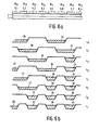
- Fig. 5a shows in sectional view a part of a charge-coupled device in the photosensitive section comprising a number of clock electrodes which, in order to distinguish them from each other, are provided with reference numerals 6,1; 6,2; 6,3; 6,4; etc.
- the voltages applies to the clock electrodes 6 vary between a high level - at which a potential well is induced in the underlying part of the channel 2 - nd a low level - at which a potential barrier is induced in the associated part of the channel.
- the charge transport is a 4-phase transport under the influence of the 4-phase clock voltages 0 ⁇ 11 , 0 ⁇ 12 , 0 ⁇ 13 and 0 ⁇ 14 .
- Fig. 5b shows the potential distribution in the channel 2 at a number of instants t. In the drawing, the positive potential is plotted in downward direction.
- the clock voltages 0 ⁇ 11 - ⁇ 14 are not applied, as usual, to all electrodes at a time, but are applied gradually thereto, as shownin Fig. 5b for the instants t 1 - t 8 .
- ⁇ 14 is applied to the electrode 6, 8, as a result of which below the electrode 6,8 the potential barrier is replaced by a well.
- 0 ⁇ 13 is applied to the electrode 6,7 as a result of which the well below the electrode 6,7 is replaced by a potential barrier and the charge packet 35 has shifted one position to the right.
- the charge packets 36, 37 and 38 have not changed their place in this period.
- the distance between the charge packets 35 and 36 is now (t 2 ) sufficiently large to also cause the charge packet 36 to participate in the charge transport without the risk of the packets being mixed.
- the charge packet 36 is shifted by one position, while the charge packets 37 and 38 remain in place.
- the distance between the packets 36 and 37 is also sufficiently large so that the packet 37 can also be transported to the right in the usual 4-phase manner simultaneously with the preceding packets 35, 36 (t 5 , t 6 ).
- the distance between the packets 37 and 38 is sufficiently large for a 4-phase transport so that the packet 38 can also be transported.
- Fig. 6a shows in the same manner as Fig. 5a a part of the charge-coupled device in the storage section or B section, while Fig. 6b shows in the same manner as Fig. 5b the associated potential distributions at a number of instants.
- the first two Figures (to, t 1 ) illustrate the situation in which the device is operated as a 4-phase CCD with four clock voltages 0 ⁇ 11 - 0 ⁇ 14 .
- the two charge packets 35 and 36 correspond to eight clock electrodes 6.
- the voltage at this clock electrode does not change any more and neither does the voltage at the clock electrode 6,8, below which a barrier has formed.
- the voltage at the clock electrode 6,6 decreases so that a barrier is also formed below this clock electrode.
- the voltage at this clock electrode further also remains constant so that the charge packet does not change its place any more.
- the charge packet 36 is stored (t 3 , t 4 ) when it has arrived below the clock electrode 6,5 in a potential well bounded on both sides by potential barriers below the clock electrodes 6,6 and 6,4.
- the charge packet 37 is stored below theclock electrode 6,3; subsequently (t 7 ) the charge packet 38 is stored below the clock electrode 6,1.
- the eight clock electrodes 6,1 - 6,8 correspond to four charge packets, which means that the information density during the storage in the storage section is twice the information density during the charge transport.
- Table 1 and Table 2 indicate how the logic state of the clock electrodes changes when an image sensed in the A section is transferred to the storage section and when the A section is then again made ready for sensing a next image.
- Table 1 indicates the situation for the even frame and Table 2 indicates the situation for the odd frame.
- the clock electrodes of the storage section are denoted by ST, A , B , C etc., ST representing the clock electrode located closest to the horizontal reading register C and controlled directly by the input signal of the shift register 8. It is assumed that together with the clock electrode ST the storage section comprises eight clock electrodes.
- the bymsol H represents the output of an additional stage of the shift register 8, which is no longer connected to a clock electrode of the storage section and with which, as will appear below, given advantages can be obtained.
- the first electrode is designated by IM.
- the following electrodes are designated by A i ...I i , the suffix i indicating that electrodes of the photo-sensitive section (image section) are concerned.
- the latter section comprises a number of electrodes exceeding by two the number of electrodes in the storage section. This difference is firstly due to the fact that the charge packets below IM often cannot be used for the image display because the geometric conditions for IM are not the same as for the remaining lines. When charge is integrated below the electrode IM, this line can be directly drained via the C register when the charge pattern is shifted from the A section to the B section.
- the first effective line is consequently located below A i or B i , depending upon the frame.
- the additional electrode is arranged at the other edge of the A section in order to ensure that the geometric conditions for the last line, i.e. the line below the electrode H i , are as equal as possible to the conditions for the remaining preceding lines.
- the storage section or B section has shifted the information of a preceding frame via the horizontal register C to the outside in the 4-phase manner described above (with extracted accordion) and that the end of the integration period is indicated by an external pulse.
- the information stored in the sensor section or A section can now be shifted on to the storage section.
- the storage section operated in a 4-phase manner is tuned to the sensor section.
- this section is operated in the accordion mode (2-phase manner), a charge packet being stored below the other electrode. According to Table 1, charge is stored below the clock electrode IM, B i , D i , F i and H i .
- the instant at which the storage section of the accordion has been fully compressed can be detected again by considering, for example, the clock electrodes G s and E s . If these electrodes have the same logic state, the storage accordion is compressed. In Table 1, this is the case at the instant t 22 , while in Table 2 this is the case at t 2 1 .
- IM When the storage accordion is compressed, IM is also applied to a fixed potential, after which the accordion of the image section is compressed. Depending upon the frame (even or odd), the logic state of IM becomes equal to 0 or 1. When this has taken place, the accordion of the photosensitive section or the A section is also compressed. The instant at which this accordion (or this part of the accordion) is compressed completely can also be detected, i.e. in that it is ascertained when, for ex-ample, the electrodes G . and I i of the photosensitive section have the same states.
- the information can be read linewise in the usual manner by means of the C register.
- the synchronization as described here can be realised for the amjor part in the system itself, independently of the frame (even or odd).
- the only external pulses (or pulses which are generated at least outside the represented part of the arrangement) which are required, are:
- Fig. 7 shows a current diagram of the control of the arrangement as described above.
- Step I For 20 msec (20.10 sec.), an image is sensed in the A section and converted into a pattern of charge packets.
- Step II By an external circuit by means of a Sync-I.C., the end of the integration is indicated by means of the VTE pulse.
- a further step is added in the shift register 7 of the storage section after the last electrode G S , but this step is no longer coupled to a clock electrode of the storage section.
- Step IV As soon as the aforementioned condition is indeed satisfied, IM is allowed to change its logic state. However, this must not be effected in an uncontrolled manner, but it must take place in phase with the 4-phase clocks in the storage section. In order to achieve this, IM is coupled to H and thus becomes effectively equal to the next CCD stage after G s .
- Step V IM now remains equal to H, while ST also continues to change until the first (effective) charge has arrived below ST. This situation can be detected as follows (see also Tables 1, 2).
- Step VII In the following stage of the current diagram, the instant is detected at which the storage accordion is completely compressed. This is the case if the electrodes E s and G s have the same state. With the given number of clock electrodes, this remains that the instant is determined at which it holds that:
- the FI pulse is again a pulse produced outside, i.e. generated outside the sensor chip or on the sensor chip, but outside the represented part of the circuit.
- Fig. 8 shows an implementation of the current diagram shown in Fig. 7.
- the shift registers 7 and 8 and the associated clock electrodes ST, A s , B s ... G , IM, A., B i ...I i are shown.
- the switches 31 are omitted in Fig. 8.
- the order of succession of the current diagram shown in Fig. 7 is maintained. It should be noted that the last inverter circuit 26 of the shift register 7 drives not a clock electrode of the storage sect on, but the point H which is used, as will appear, for driving IM.
- the signal VTE is supplied from the outside, as a result of which it becomes possible to transfer the stored information from the photosensitive section to the storage section.
- the output signals of the AND gates 41 and 45 are supplied to the inputs of the OR gate 46, which produces as output signal a 1, if either the output of 41 or the output of 45 produces a 1.
- the output signal of the OR gate 46 is supplied to the input of the AND gate 47.
- the signal VTE is supplied to the second input of the AND gate 47.
- the AND gate 47 comprises a third input which is connected to the output of an inverter circuit 48, to whose input the clock signal 0 ⁇ 1 is supplied.
- the signal IMT not only controls the clock electrode, but is also supplied to the clock electrode ST via the OR gate 56.
- the signal IMT can simply be supplied via a conductive connection to the OR gate 56. For the sake of clarity of the drawing, this connection is omitted and is replaced by an arrow IMT at the OR gate 56.
- condition of the flipflop 49 does not change any more when 0 ⁇ 1 is clocked.
- This condition can be detected by means of the AND gate 53, of which two inputs are connected to the clock electrodes I i and H . .
- a third input of the AND gate 53 is connected to the output of an inverter circuit 54, to whose input the clock signal 0 ⁇ 2 is supplied.
- the output signal of the AND gate 53 is supplied to the S input of the RS flipflop 55.
- the signal STC can again be supplied to the OR gate 56 via a usual connection, which, however, is not shown in Fig. 8 for the sake of clarity.
- the output signal of the gate 57 is preferably supplied together with the 0 ⁇ 1 signal inverted by the inverter circuit 48 via the AND gate 58 to the flipflop 49.
- This signal is supplied to the R input (reset input) of the flipflop 49.
- Due to the fact that Q becomes 0, the AND gate 50 no longer transmits the signals H to the clock electrode IM.
- the latter can now also be applied to a fixed potential in order to also compress the photosensitive accordion.
- the condition to which IM and hence also the whole photosensitive accordion is set is frame-dependent, however.
- a signal FI field identification
- FI field identification
- the Q output then passes again to 0.
- the photosensitive accordion is now completely compressed, which means that the photo- sensitive section of the sensor is ready to form a new frame of image information. Meanwhile, the information stored in the storage section can be read linewise.
- the OR gate 56 whose inputs STC and IMT are both at "0" is provided with a third input 62, via which the externally generated signal STH (input storage hutling) is supplied to the clock electrode ST and which renders it possible for an image line stored below the clock electrode ST to be transferred to the horizontal C register.
- This trns- port can take place again in the samen manner, though at a lower frequency, as the transport described above, an increasingly larger part of the storage accordion participating in the 4-phase transport.
- the signal VTE can be supplied again, while (via the same input as that via which the signal STH is supplied) a clock signal is supplied having a comparatively high frequency, whereupon the cycle described here starts again.
- the gates and flipflops present in the circuit shown in Fig. 8 may all be of a generally known configuration.
- the circuit may be entirely manufactured in C-MOS technology according to Fig. 2 and may be integrated together with the sensor and the shift registers 7 and 8 in one common semiconductor body 10.
- each electrode may be in the form of a storage section and a transfer section, while, when a common voltage is applied, a potential well is induced below the storage section and a potential barrier is induced below the transfer section in the charge transport channel.
- the invention may further be used besides in the type of sensors described here in other charge-coupled devices with the accordion mode of operation.
- the clock electrodes instead of being directly biased by the shift register 7, 8 the clock electrodes may be connected to switches which connect the electrodes either to a point at a fixed voltage or to a point at a varying voltage, as described, for example, in Netherlands Patent Application No. 8301977 (PHN 10 698) in the name of the Applicant.
- the invention may also be used in sensors of the interline type or line sensors, which are operated according to the accordion principle described here.
Landscapes
- Engineering & Computer Science (AREA)
- Multimedia (AREA)
- Signal Processing (AREA)
- Solid State Image Pick-Up Elements (AREA)
- Transforming Light Signals Into Electric Signals (AREA)
- Studio Devices (AREA)
- Image-Pickup Tubes, Image-Amplification Tubes, And Storage Tubes (AREA)
- Details Of Cameras Including Film Mechanisms (AREA)
Priority Applications (1)
| Application Number | Priority Date | Filing Date | Title |
|---|---|---|---|
| AT86200710T ATE59511T1 (de) | 1985-04-29 | 1986-04-25 | Ladungsgekoppelte anordnung und diese anordnung umfassende kamera. |
Applications Claiming Priority (2)
| Application Number | Priority Date | Filing Date | Title |
|---|---|---|---|
| NL8501210A NL8501210A (nl) | 1985-04-29 | 1985-04-29 | Ladingsgekoppelde inrichting. |
| NL8501210 | 1985-04-29 |
Publications (2)
| Publication Number | Publication Date |
|---|---|
| EP0200270A1 true EP0200270A1 (de) | 1986-11-05 |
| EP0200270B1 EP0200270B1 (de) | 1990-12-27 |
Family
ID=19845895
Family Applications (1)
| Application Number | Title | Priority Date | Filing Date |
|---|---|---|---|
| EP86200710A Expired - Lifetime EP0200270B1 (de) | 1985-04-29 | 1986-04-25 | Ladungsgekoppelte Anordnung und diese Anordnung umfassende Kamera |
Country Status (10)
| Country | Link |
|---|---|
| US (1) | US4723168A (de) |
| EP (1) | EP0200270B1 (de) |
| JP (1) | JPS61252770A (de) |
| KR (1) | KR860008680A (de) |
| AT (1) | ATE59511T1 (de) |
| AU (1) | AU588588B2 (de) |
| CA (1) | CA1256200A (de) |
| DE (1) | DE3676542D1 (de) |
| ES (1) | ES8800558A1 (de) |
| NL (1) | NL8501210A (de) |
Cited By (1)
| Publication number | Priority date | Publication date | Assignee | Title |
|---|---|---|---|---|
| EP0275576A1 (de) * | 1986-11-27 | 1988-07-27 | Koninklijke Philips Electronics N.V. | Ladungsgekoppelte Anordnung |
Families Citing this family (6)
| Publication number | Priority date | Publication date | Assignee | Title |
|---|---|---|---|---|
| US4991016A (en) * | 1987-11-27 | 1991-02-05 | U.S. Philips Corp. | Control method for a frame transfer sensor in an image pick-up device to obtain black level information in a picture signal, and image pick-up device suitable for use of said method |
| US4862275A (en) * | 1988-10-27 | 1989-08-29 | Eastman Kodak Company | Readout of charge packets from area imager CCD using an inverter-chain shift register |
| GB8901200D0 (en) * | 1989-01-19 | 1989-03-15 | Eev Ltd | Camera using imaging array |
| JP3560240B2 (ja) * | 2002-01-18 | 2004-09-02 | ソニー株式会社 | Ccd撮像素子 |
| KR101034525B1 (ko) * | 2003-06-26 | 2011-05-12 | 코닌클리즈케 필립스 일렉트로닉스 엔.브이. | 통합 디스플레이 유닛 |
| KR102299662B1 (ko) * | 2017-07-13 | 2021-09-07 | 매그나칩 반도체 유한회사 | 반도체 소자 및 그 제조 방법 |
Citations (2)
| Publication number | Priority date | Publication date | Assignee | Title |
|---|---|---|---|---|
| US4178614A (en) * | 1978-08-24 | 1979-12-11 | Rca Corporation | Readout of a densely packed CCD |
| EP0128615A1 (de) * | 1983-06-03 | 1984-12-19 | Koninklijke Philips Electronics N.V. | Ladungsgekoppelte Halbleiter-Anordnung und Bildsensor mit hoher Informationsdichte |
Family Cites Families (4)
| Publication number | Priority date | Publication date | Assignee | Title |
|---|---|---|---|---|
| NL8401311A (nl) * | 1984-04-24 | 1985-11-18 | Philips Nv | Ladingsgekoppelde halfgeleiderinrichting met dynamische besturing. |
| US4574313A (en) * | 1984-12-12 | 1986-03-04 | Rca Corporation | Cascaded CCD shift registers having different numbers of clocking phases |
| US4575763A (en) * | 1984-12-12 | 1986-03-11 | Rca Corporation | CCD with number of clocking signal phases increasing in later charge transfer stages |
| US4580169A (en) * | 1984-12-12 | 1986-04-01 | Rca Corporation | CCD imager with photoconversion in an image register clocked with a reduced number of clock phases during image transfer |
-
1985
- 1985-04-29 NL NL8501210A patent/NL8501210A/nl not_active Application Discontinuation
-
1986
- 1986-04-21 US US06/856,568 patent/US4723168A/en not_active Expired - Fee Related
- 1986-04-24 CA CA000507480A patent/CA1256200A/en not_active Expired
- 1986-04-25 ES ES554374A patent/ES8800558A1/es not_active Expired
- 1986-04-25 DE DE8686200710T patent/DE3676542D1/de not_active Expired - Lifetime
- 1986-04-25 AT AT86200710T patent/ATE59511T1/de not_active IP Right Cessation
- 1986-04-25 EP EP86200710A patent/EP0200270B1/de not_active Expired - Lifetime
- 1986-04-26 JP JP61095923A patent/JPS61252770A/ja active Granted
- 1986-04-26 KR KR1019860003231A patent/KR860008680A/ko not_active Withdrawn
- 1986-04-28 AU AU56771/86A patent/AU588588B2/en not_active Ceased
Patent Citations (2)
| Publication number | Priority date | Publication date | Assignee | Title |
|---|---|---|---|---|
| US4178614A (en) * | 1978-08-24 | 1979-12-11 | Rca Corporation | Readout of a densely packed CCD |
| EP0128615A1 (de) * | 1983-06-03 | 1984-12-19 | Koninklijke Philips Electronics N.V. | Ladungsgekoppelte Halbleiter-Anordnung und Bildsensor mit hoher Informationsdichte |
Cited By (2)
| Publication number | Priority date | Publication date | Assignee | Title |
|---|---|---|---|---|
| EP0275576A1 (de) * | 1986-11-27 | 1988-07-27 | Koninklijke Philips Electronics N.V. | Ladungsgekoppelte Anordnung |
| AU607724B2 (en) * | 1986-11-27 | 1991-03-14 | N.V. Philips Gloeilampenfabrieken | Charge-coupled device |
Also Published As
| Publication number | Publication date |
|---|---|
| JPS61252770A (ja) | 1986-11-10 |
| EP0200270B1 (de) | 1990-12-27 |
| ES8800558A1 (es) | 1987-11-01 |
| KR860008680A (ko) | 1986-11-17 |
| CA1256200A (en) | 1989-06-20 |
| AU588588B2 (en) | 1989-09-21 |
| JPH0343828B2 (de) | 1991-07-03 |
| NL8501210A (nl) | 1986-11-17 |
| ATE59511T1 (de) | 1991-01-15 |
| DE3676542D1 (de) | 1991-02-07 |
| AU5677186A (en) | 1986-11-06 |
| ES554374A0 (es) | 1987-11-01 |
| US4723168A (en) | 1988-02-02 |
Similar Documents
| Publication | Publication Date | Title |
|---|---|---|
| EP0468034B1 (de) | Selektiver betrieb einer zwischenzeilig übertragenden ccd-bildsensorvorrichtung in verschachtelten und nichtverschachtelten moden | |
| CA1068395A (en) | Charge coupled imager | |
| US4816916A (en) | CCD area image sensor operable in both of line-sequential and interlace scannings and a method for operating the same | |
| US4928158A (en) | Solid-state image sensor having a plurality of horizontal transfer portions | |
| US4744057A (en) | Multilinear charge transfer array | |
| US4540901A (en) | Image-sensing charge-coupled device with both high-speed and low-speed read-outs | |
| EP0193977B1 (de) | Ladungsgekoppelte Bildsensoranordnung | |
| WO1991015079A1 (en) | Image sensor | |
| US5280186A (en) | CCD image sensor with four phase clocking mechanism | |
| EP0200270B1 (de) | Ladungsgekoppelte Anordnung und diese Anordnung umfassende Kamera | |
| AU603159B2 (en) | Ccd image sensor arrangement | |
| AU607724B2 (en) | Charge-coupled device | |
| EP0492182B1 (de) | Festkörper-Bildsensor | |
| EP0161023B1 (de) | Ladungsgekoppelte Halbleiteranordnung mit dynamischer Steuerung | |
| EP0128615B1 (de) | Ladungsgekoppelte Halbleiter-Anordnung und Bildsensor mit hoher Informationsdichte | |
| KR970010687B1 (ko) | 쌍방형 전하결합소자 | |
| US5091922A (en) | Charge transfer device type solid state image sensor having constant saturation level | |
| JPS58175372A (ja) | 固体撮像素子 | |
| JPH063959B2 (ja) | 固体イメ−ジセンサ | |
| JPH0433143B2 (de) | ||
| JPH02192371A (ja) | 電荷結合型固体撮像装置 | |
| JPS60251781A (ja) | 電荷転送撮像装置の駆動方法 | |
| JPS59165452A (ja) | 電荷転送型固体撮像素子 | |
| JPH05176234A (ja) | 固体撮像装置 | |
| JPH06268927A (ja) | 固体撮像装置 |
Legal Events
| Date | Code | Title | Description |
|---|---|---|---|
| PUAI | Public reference made under article 153(3) epc to a published international application that has entered the european phase |
Free format text: ORIGINAL CODE: 0009012 |
|
| AK | Designated contracting states |
Kind code of ref document: A1 Designated state(s): AT BE CH DE FR GB IT LI NL SE |
|
| 17P | Request for examination filed |
Effective date: 19870504 |
|
| 17Q | First examination report despatched |
Effective date: 19890523 |
|
| GRAA | (expected) grant |
Free format text: ORIGINAL CODE: 0009210 |
|
| AK | Designated contracting states |
Kind code of ref document: B1 Designated state(s): AT BE CH DE FR GB IT LI NL SE |
|
| PG25 | Lapsed in a contracting state [announced via postgrant information from national office to epo] |
Ref country code: IT Free format text: LAPSE BECAUSE OF FAILURE TO SUBMIT A TRANSLATION OF THE DESCRIPTION OR TO PAY THE FEE WITHIN THE PRE;WARNING: LAPSES OF ITALIAN PATENTS WITH EFFECTIVE DATE BEFORE 2007 MAY HAVE OCCURRED AT ANY TIME BEFORE 2007. THE CORRECT EFFECTIVE DATE MAY BE DIFFERENT FROM THE ONE RECORDED.SCRIBED TIME-LIMIT Effective date: 19901227 Ref country code: NL Effective date: 19901227 Ref country code: FR Effective date: 19901227 Ref country code: AT Effective date: 19901227 Ref country code: BE Effective date: 19901227 |
|
| REF | Corresponds to: |
Ref document number: 59511 Country of ref document: AT Date of ref document: 19910115 Kind code of ref document: T |
|
| REF | Corresponds to: |
Ref document number: 3676542 Country of ref document: DE Date of ref document: 19910207 |
|
| PG25 | Lapsed in a contracting state [announced via postgrant information from national office to epo] |
Ref country code: GB Effective date: 19910425 |
|
| PG25 | Lapsed in a contracting state [announced via postgrant information from national office to epo] |
Ref country code: SE Effective date: 19910426 |
|
| PG25 | Lapsed in a contracting state [announced via postgrant information from national office to epo] |
Ref country code: CH Effective date: 19910430 Ref country code: LI Effective date: 19910430 |
|
| NLV1 | Nl: lapsed or annulled due to failure to fulfill the requirements of art. 29p and 29m of the patents act | ||
| EN | Fr: translation not filed | ||
| PLBE | No opposition filed within time limit |
Free format text: ORIGINAL CODE: 0009261 |
|
| STAA | Information on the status of an ep patent application or granted ep patent |
Free format text: STATUS: NO OPPOSITION FILED WITHIN TIME LIMIT |
|
| 26N | No opposition filed | ||
| REG | Reference to a national code |
Ref country code: CH Ref legal event code: PL |
|
| GBPC | Gb: european patent ceased through non-payment of renewal fee | ||
| PG25 | Lapsed in a contracting state [announced via postgrant information from national office to epo] |
Ref country code: DE Effective date: 19920201 |
|
| EUG | Se: european patent has lapsed |
Ref document number: 86200710.1 Effective date: 19911108 |