EP0205122A2 - Ereigniszählervoruntersetzer - Google Patents
Ereigniszählervoruntersetzer Download PDFInfo
- Publication number
- EP0205122A2 EP0205122A2 EP86107717A EP86107717A EP0205122A2 EP 0205122 A2 EP0205122 A2 EP 0205122A2 EP 86107717 A EP86107717 A EP 86107717A EP 86107717 A EP86107717 A EP 86107717A EP 0205122 A2 EP0205122 A2 EP 0205122A2
- Authority
- EP
- European Patent Office
- Prior art keywords
- event
- address
- count number
- count
- memory
- Prior art date
- Legal status (The legal status is an assumption and is not a legal conclusion. Google has not performed a legal analysis and makes no representation as to the accuracy of the status listed.)
- Withdrawn
Links
Images
Classifications
-
- G—PHYSICS
- G06—COMPUTING OR CALCULATING; COUNTING
- G06F—ELECTRIC DIGITAL DATA PROCESSING
- G06F11/00—Error detection; Error correction; Monitoring
- G06F11/30—Monitoring
- G06F11/34—Recording or statistical evaluation of computer activity, e.g. of down time, of input/output operation ; Recording or statistical evaluation of user activity, e.g. usability assessment
- G06F11/3466—Performance evaluation by tracing or monitoring
- G06F11/348—Circuit details, i.e. tracer hardware
-
- G—PHYSICS
- G06—COMPUTING OR CALCULATING; COUNTING
- G06F—ELECTRIC DIGITAL DATA PROCESSING
- G06F2201/00—Indexing scheme relating to error detection, to error correction, and to monitoring
- G06F2201/86—Event-based monitoring
-
- G—PHYSICS
- G06—COMPUTING OR CALCULATING; COUNTING
- G06F—ELECTRIC DIGITAL DATA PROCESSING
- G06F2201/00—Indexing scheme relating to error detection, to error correction, and to monitoring
- G06F2201/88—Monitoring involving counting
Definitions
- the present invention relates to event counters and in particular to a method and apparatus for prescaling an event count.
- the code under test was modified to include subroutines which updated a stored count each time a selected memory address was generated.
- This intrusive approach is difficult to utilize because it requires an intimate knowledge of the code being tested in order to modify it.
- Another approach is to connect a word recognizer to the address bus of the microprocessor and to program the word recognizer to generate a pulse each time a selected address appears on the bus. The pulses are then counted by a conventional counter.
- This method is nonintrusive since the code under test is not modified, and is therefore often easier to perform and less prone to error.
- this method requires a large number of word recognizers and counters.
- the address bus of a computer under test could also be applied as a data input to a test computer which could be programmed to count occurrences of selected addresses, eliminating the need for large numbers of counters and word recognizers, but such a method would require the use of a very high speed, costly test computer.
- an apparatus for counting and prescaling events characterized by unique numbers appearing on a bus comprises a random access memory (RAM), a latch and an adder.
- the bus is applied to address the RAM according to the event number appearing thereon.
- the RAM places on a data output bus to the latch count data stored at the current address.
- the latch transmits this count data to the adder which increments the count data by one and then places the incremented count data on a data input bus to the RAM.
- the incremented count data is written into the RAM at the current event number address.
- the count data stored in the RAM at an address matching the event number is incremented by one. Therefore each storage address in the RAM contains a count of the number of times the corresponding event number has appeared on the bus since the data stored in the RAM was initialized to zero.
- a buffer is provided to store the current event number whenever the adder overflows (its output returns to zero) as a result of a count.
- event numbers may be stored in the buffer for subsequent retrieval by an external controller at a rate that is lower than the data input rate to the prescaler and at idle moments when the controller is not performing other tasks.
- the controller retrieves an event number from the buffer, the controller can ascertain the event has been counted a fixed number of times and can increment an internally stored count in its own memory which may be denser and slower but cheaper than the RAM of the prescaler.
- a first multiplexer is provided to switch the address input to the RAM from the event number bus to another bus carrying an address from the external controller.
- the controller also has access to the RAM data output bus and controls the switching operation of the multiplexer. By switching the multiplexer the external controller can address the RAM so that it may read the current event count stored at any RAM address.
- a second multiplexer controlled by the external controller is provided to switch the data input to the adder from the latch output to a minus one.
- the external controller can then reset to zero the count stored at any RAM address by applying the minus one to the adder which then places a zero on the data input terminals of the RAM. The zero is then written into the RAM at an address determined by the controller, thereby resetting the count.
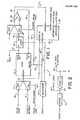
- an event counter 10 adapted to count occurrences of events characterized by unique binary event numbers, such as addresses appearing on a bus.
- An event number carried on bus 12, is applied to one input of a first multiplexer 14.
- the output terminals of multiplexer 14 are connected by a bus 15 to addressing terminals of a random access memory (RAM) 16.
- the RAM 16 stores a separate event count for each event at an address corresponding to the event number.
- RAM 16 is addressed during a read operation, the event count data stored at the current address appears on data output bus 18 connected to a data input of a latch 20.
- multiplexer 14 is switched to a state wherein an event number appearing on bus 12 is applied to address RAM 16, which is normally in a read mode unless a WRITE control input is asserted.
- This WRITE control input is initially not asserted, so an event count data stored at an address matching the event number on bus 12 is initially placed on data output bus 18.
- Multiplexer 24 is normally switched such that the event count data on bus 22 passes through the multiplexer and over bus 26 to adder 28 where it is incremented by one and further passed over the data input bus 30 to the RAM 16 data input.
- the WRITE control input of the RAM 16 is then strobed whereby the incremented event count data appearing on bus 30 is written into RAM 16 at the current event number address, replacing the existing event count.
- the count data stored at any address in the RAM 16 may be read by an external controller.
- a bus 32 from the external controller is applied to another input of first multiplexer 14 while a read/count control line 34 from the controller, applied to a SELECT input of the multiplexer 14, controls the switching state of the multiplexer.
- the read/count control line is asserted, and multiplexer 14 applies addressing data carried on bus 32 from the controller to address RAM 16.
- the data stored in RAM 16 then appears on data output bus 18 which carries the data to the external controller. In this operation, however, the WRITE control input to the RAM 16 is not asserted and any data appearing on RAM data input bus 30 is not written into the RAM.
- the external controller may initialize (zero) the count data stored at any address in the RAM 16. To do so, the address of the data to be initialized is placed on bus 32 and a READ/COUNT control input on line 34 applied to the SELECT input of the first multiplexer 14 is asserted whereby the multiplexer passes the address on to the address input of RAM 16.
- a CLEAR control line 35 from the external controller controls the switching position of the second multiplexer 24, and also asserts the WRITE control input of RAM 16 through a diode 42.
- a minus one (-1) is applied to a second input of multiplexer 24 so that when the CLEAR line is asserted, multiplexer 24 transmits the minus one to the ADDER 28 over bus 26 rather than the current RAM 16 data output.
- the adder 28 then sums the minus one input with the plus one input to produce a zero output on the RAM 16 data input bus 30 and this zero value is then written into RAM 16 at the current event number address to initialize the count for the associated event number as the CLEAR line 35 is deasserted.
- a buffer 36 which may be of the last-in, first-out or first-in, first-out type, is provided to store event numbers when the adder 28 overflows, i.e. when as a result of a count the adder output changes from a maximum number to a zero.
- Adder 28 asserts an overflow output line 29 whenever this happens and this overflow output line 29 is applied to a PUSH input of buffer 36.
- RAM 16 data input bus 15, carrying the event number, is also connected to a DATA IN input of buffer 36.
- the PUSH input is asserted by the overflow line 29 output of adder 28, the current event number on bus 15 is stored in buffer 36 on receipt of a pulse on a CLOCK input to buffer 36.
- a single-bit, NOT EMPTY output signal of buffer 36 is asserted and transmitted to the controller whenever the buffer contains one or more event numbers.
- the external controller may then read an event number stored in buffer 36 by asserting a POP input thereto and the data then appears on a buffer data output bus 38 connected to the controller.
- Buffer 36 permits event counter 10 to count continuously, acting as a count prescaler for the external controller. Each time adder 28 reaches its limit for a particular event number count, the count in RAM 16 resets to zero and the event number is stored in buffer 36 until read by the controller. When the controller reads such a number, it knows that the event has been counted a fixed number of times. When the counting process ends, the controller can read the remaining count stored in RAM 16 to update the final count result for any event number and can then reset the count.
- a count sequencing circuit 40 provides the necessary timing for the clocking of the latch 20 and the buffer 36 and for the assertion of the WRITE control input of RAM 16 during a count operation.
- One output line 46 of sequencer 40 is applied to the clock input of latch 20, while a second output line 48 is applied to the clock input of buffer 36 and through a diode 44 to the write control input of RAM 16.
- Diodes 42 and 44 are provided to isolate the CLEAR control line from the sequencer 40 write control output.
- a COUNT pulse from a device under test is applied to an input of sequencer 40 when an event number appearing on bus 12 is valid and the event is ready to be counted.
- a signal is typically available on a read/write control line of a microprocessor when the event numbers to be counted comprise addresses appearing on the microprocessor address bus.
- the sequencer 40 waits for a time sufficient for the RAM 16 to place the count data on output bus 18 to latch 20, and then asserts output line 46, causing latch 20 to pass the count data to adder 28.
- the sequencer 40 transmits a pulse on output line 48 causing RAM 16 to write the new data to the current address.
- the pulse on line 48 is applied to the clock input of buffer 36 so that if the adder 28 happens to overflow as a result of the count and generates a PUSH signal, the current event number on bus 15 is stored in the buffer 36.
- An embodiment of the count sequencing circuit 40 depicted in block diagram form in FIG. 2, comprises a two stage delay line 50.
- the COUNT pulse is applied to one end of the delay line.
- Output line 46 is tapped from the delay line after the first stage 52, and output line 48 is tapped after the second stage 54.
- the first stage is sized to delay the COUNT pulse for at least as long as the RAM access time, while the second stage is sized to delay the COUNT pulse for at least as long as the adder 28 operating time.
- the present invention is capable of maintaining simultaneous counts of a plurality of events characterized by unique event numbers and is also capable of continuous operation as an event count prescaler for an external controller. While a preferred embodiment of the present invention has been shown and described, it will be apparent to those skilled in the art that many changes and modifications may be made without departing from the invention in its broader aspects. The appended claims are therefore intended to cover all such changes and modifications as fall within the true spirit and scope of the invention.
Landscapes
- Engineering & Computer Science (AREA)
- General Engineering & Computer Science (AREA)
- Theoretical Computer Science (AREA)
- Computer Hardware Design (AREA)
- Quality & Reliability (AREA)
- Physics & Mathematics (AREA)
- General Physics & Mathematics (AREA)
- Debugging And Monitoring (AREA)
Applications Claiming Priority (2)
| Application Number | Priority Date | Filing Date | Title |
|---|---|---|---|
| US744581 | 1985-06-13 | ||
| US06/744,581 US4849924A (en) | 1985-06-13 | 1985-06-13 | Event counting prescaler |
Publications (2)
| Publication Number | Publication Date |
|---|---|
| EP0205122A2 true EP0205122A2 (de) | 1986-12-17 |
| EP0205122A3 EP0205122A3 (de) | 1989-04-05 |
Family
ID=24993235
Family Applications (1)
| Application Number | Title | Priority Date | Filing Date |
|---|---|---|---|
| EP86107717A Withdrawn EP0205122A3 (de) | 1985-06-13 | 1986-06-06 | Ereigniszählervoruntersetzer |
Country Status (4)
| Country | Link |
|---|---|
| US (1) | US4849924A (de) |
| EP (1) | EP0205122A3 (de) |
| JP (1) | JPS61286940A (de) |
| CA (1) | CA1258715A (de) |
Cited By (3)
| Publication number | Priority date | Publication date | Assignee | Title |
|---|---|---|---|---|
| AU609284B2 (en) * | 1988-04-25 | 1991-04-26 | Nec Corporation | Data processing apparatus |
| EP0395281A3 (de) * | 1989-04-27 | 1992-11-25 | Digital Equipment Corporation | Verfahren und Vorrichtung zum Verbinden von Diagnoseinformationen mit spezifischen Rechnerbefehlen |
| EP0990993A1 (de) * | 1998-07-28 | 2000-04-05 | Bull S.A. | Ereigniszähler |
Families Citing this family (4)
| Publication number | Priority date | Publication date | Assignee | Title |
|---|---|---|---|---|
| US5233545A (en) * | 1989-09-19 | 1993-08-03 | Hewlett-Packard Company | Time interval triggering and hardware histogram generation |
| US4979177A (en) * | 1989-10-26 | 1990-12-18 | Tektronix, Inc. | Enhanced counter/timer resolution in a logic analyzer |
| JP6347055B2 (ja) * | 2014-03-28 | 2018-06-27 | パナソニックIpマネジメント株式会社 | 不揮発性メモリ装置 |
| US10691511B2 (en) * | 2018-09-19 | 2020-06-23 | Arm Limited | Counting events from multiple sources |
Family Cites Families (10)
| Publication number | Priority date | Publication date | Assignee | Title |
|---|---|---|---|---|
| FR1538083A (fr) * | 1966-09-28 | 1968-08-30 | Ibm | Dispositif arithmétique |
| US3564227A (en) * | 1967-12-14 | 1971-02-16 | Potter Instrument Co Inc | Computer and accumulator therefor incorporating push down register |
| US3538318A (en) * | 1968-08-21 | 1970-11-03 | Hughes Aircraft Co | Wear weighting function generator for the determination of the proper aiming of a gun |
| US3697695A (en) * | 1970-12-09 | 1972-10-10 | Uwe A Pommerening | Call metering for telephone exchange |
| US3771144A (en) * | 1972-07-24 | 1973-11-06 | Ibm | Clock for computer performance measurements |
| JPS525565A (en) * | 1975-07-02 | 1977-01-17 | Toshiba Corp | Electric clock circuit |
| US4016545A (en) * | 1975-07-31 | 1977-04-05 | Harris Corporation | Plural memory controller apparatus |
| JPS55163697A (en) * | 1979-06-05 | 1980-12-19 | Mitsubishi Electric Corp | Memory device |
| US4445414A (en) * | 1982-02-24 | 1984-05-01 | Apple Computer, Inc. | Digital, simultaneous, discrete frequency generator |
| JPS6014358A (ja) * | 1983-07-04 | 1985-01-24 | Nec Corp | 情報収集装置 |
-
1985
- 1985-06-13 US US06/744,581 patent/US4849924A/en not_active Expired - Fee Related
-
1986
- 1986-06-06 EP EP86107717A patent/EP0205122A3/de not_active Withdrawn
- 1986-06-10 JP JP61134732A patent/JPS61286940A/ja active Pending
- 1986-06-11 CA CA000511322A patent/CA1258715A/en not_active Expired
Cited By (3)
| Publication number | Priority date | Publication date | Assignee | Title |
|---|---|---|---|---|
| AU609284B2 (en) * | 1988-04-25 | 1991-04-26 | Nec Corporation | Data processing apparatus |
| EP0395281A3 (de) * | 1989-04-27 | 1992-11-25 | Digital Equipment Corporation | Verfahren und Vorrichtung zum Verbinden von Diagnoseinformationen mit spezifischen Rechnerbefehlen |
| EP0990993A1 (de) * | 1998-07-28 | 2000-04-05 | Bull S.A. | Ereigniszähler |
Also Published As
| Publication number | Publication date |
|---|---|
| EP0205122A3 (de) | 1989-04-05 |
| CA1258715A (en) | 1989-08-22 |
| JPS61286940A (ja) | 1986-12-17 |
| US4849924A (en) | 1989-07-18 |
Similar Documents
| Publication | Publication Date | Title |
|---|---|---|
| US4835675A (en) | Memory unit for data tracing | |
| EP0395210B1 (de) | Schwellendetektionsschaltungen für digitale Pufferspeicher | |
| US5850512A (en) | Bus analyzer and method for testing internal data paths thereof | |
| US4752928A (en) | Transaction analyzer | |
| EP0159588B1 (de) | Logikanalysator | |
| US4835736A (en) | Data acquisition system for capturing and storing clustered test data occurring before and after an event of interest | |
| US4536646A (en) | Time accounting system | |
| US4774681A (en) | Method and apparatus for providing a histogram | |
| US4550387A (en) | Circuit for detecting the occurrence of a plurality of signals in a predetermined sequence | |
| US4696005A (en) | Apparatus for reducing test data storage requirements for high speed VLSI circuit testing | |
| US4849924A (en) | Event counting prescaler | |
| KR870003431A (ko) | 데이타 처리장치 | |
| CA1266130A (en) | Circular first-in, first-out buffer | |
| EP0297398A2 (de) | Steuerkreis für Verarbeitungsimpulse | |
| US4748556A (en) | Variable tracking word recognizer for detecting the occurrence of a dynamic-variable address | |
| EP0589662A2 (de) | Digitalsignalverarbeitungssystem | |
| US5089955A (en) | Programmable counter/timer device with programmable registers having programmable functions | |
| EP0463640A2 (de) | Speicheranordnung zur Simulation eines Schieberegisters | |
| US4970679A (en) | Pulse input apparatus | |
| US4918647A (en) | Programmable interface unit which generates dedicated control signals in response to a single control word | |
| US4195339A (en) | Sequential control system | |
| GB2168225A (en) | Signal controlled waveform recorder | |
| GB2099618A (en) | Algorithmic word generator | |
| US4562534A (en) | Data processing system having a control device for controlling an intermediate memory during a bulk data transport between a source device and a destination device | |
| USRE34843E (en) | Signal controlled waveform recorder |
Legal Events
| Date | Code | Title | Description |
|---|---|---|---|
| PUAI | Public reference made under article 153(3) epc to a published international application that has entered the european phase |
Free format text: ORIGINAL CODE: 0009012 |
|
| AK | Designated contracting states |
Kind code of ref document: A2 Designated state(s): DE FR GB IT NL |
|
| PUAL | Search report despatched |
Free format text: ORIGINAL CODE: 0009013 |
|
| AK | Designated contracting states |
Kind code of ref document: A3 Designated state(s): DE FR GB IT NL |
|
| STAA | Information on the status of an ep patent application or granted ep patent |
Free format text: STATUS: THE APPLICATION IS DEEMED TO BE WITHDRAWN |
|
| 18D | Application deemed to be withdrawn |
Effective date: 19891006 |
|
| RIN1 | Information on inventor provided before grant (corrected) |
Inventor name: ABLEIDINGER, BRUCE Inventor name: PROVIDENZA, JOHN R. |