EP0205158B1 - Commutateur électronique - Google Patents
Commutateur électronique Download PDFInfo
- Publication number
- EP0205158B1 EP0205158B1 EP86107922A EP86107922A EP0205158B1 EP 0205158 B1 EP0205158 B1 EP 0205158B1 EP 86107922 A EP86107922 A EP 86107922A EP 86107922 A EP86107922 A EP 86107922A EP 0205158 B1 EP0205158 B1 EP 0205158B1
- Authority
- EP
- European Patent Office
- Prior art keywords
- mosfet
- fet
- source
- drain
- terminal
- Prior art date
- Legal status (The legal status is an assumption and is not a legal conclusion. Google has not performed a legal analysis and makes no representation as to the accuracy of the status listed.)
- Expired - Lifetime
Links
- 230000000295 complement effect Effects 0.000 claims description 2
- 108091006146 Channels Proteins 0.000 description 2
- 102000004129 N-Type Calcium Channels Human genes 0.000 description 1
- 108090000699 N-Type Calcium Channels Proteins 0.000 description 1
- 230000001419 dependent effect Effects 0.000 description 1
- 230000008021 deposition Effects 0.000 description 1
- 238000011161 development Methods 0.000 description 1
- 230000018109 developmental process Effects 0.000 description 1
Images
Classifications
-
- H—ELECTRICITY
- H03—ELECTRONIC CIRCUITRY
- H03K—PULSE TECHNIQUE
- H03K17/00—Electronic switching or gating, i.e. not by contact-making and –breaking
- H03K17/51—Electronic switching or gating, i.e. not by contact-making and –breaking characterised by the components used
- H03K17/56—Electronic switching or gating, i.e. not by contact-making and –breaking characterised by the components used by the use, as active elements, of semiconductor devices
- H03K17/687—Electronic switching or gating, i.e. not by contact-making and –breaking characterised by the components used by the use, as active elements, of semiconductor devices the devices being field-effect transistors
- H03K17/6871—Electronic switching or gating, i.e. not by contact-making and –breaking characterised by the components used by the use, as active elements, of semiconductor devices the devices being field-effect transistors the output circuit comprising more than one controlled field-effect transistor
- H03K17/6872—Electronic switching or gating, i.e. not by contact-making and –breaking characterised by the components used by the use, as active elements, of semiconductor devices the devices being field-effect transistors the output circuit comprising more than one controlled field-effect transistor using complementary field-effect transistors
-
- H—ELECTRICITY
- H03—ELECTRONIC CIRCUITRY
- H03K—PULSE TECHNIQUE
- H03K19/00—Logic circuits, i.e. having at least two inputs acting on one output; Inverting circuits
- H03K19/02—Logic circuits, i.e. having at least two inputs acting on one output; Inverting circuits using specified components
- H03K19/08—Logic circuits, i.e. having at least two inputs acting on one output; Inverting circuits using specified components using semiconductor devices
- H03K19/094—Logic circuits, i.e. having at least two inputs acting on one output; Inverting circuits using specified components using semiconductor devices using field-effect transistors
- H03K19/0944—Logic circuits, i.e. having at least two inputs acting on one output; Inverting circuits using specified components using semiconductor devices using field-effect transistors using MOSFET or insulated gate field-effect transistors, i.e. IGFET
- H03K19/09441—Logic circuits, i.e. having at least two inputs acting on one output; Inverting circuits using specified components using semiconductor devices using field-effect transistors using MOSFET or insulated gate field-effect transistors, i.e. IGFET of the same canal type
- H03K19/09446—Logic circuits, i.e. having at least two inputs acting on one output; Inverting circuits using specified components using semiconductor devices using field-effect transistors using MOSFET or insulated gate field-effect transistors, i.e. IGFET of the same canal type using only depletion transistors
-
- H—ELECTRICITY
- H03—ELECTRONIC CIRCUITRY
- H03K—PULSE TECHNIQUE
- H03K19/00—Logic circuits, i.e. having at least two inputs acting on one output; Inverting circuits
- H03K19/02—Logic circuits, i.e. having at least two inputs acting on one output; Inverting circuits using specified components
- H03K19/08—Logic circuits, i.e. having at least two inputs acting on one output; Inverting circuits using specified components using semiconductor devices
- H03K19/094—Logic circuits, i.e. having at least two inputs acting on one output; Inverting circuits using specified components using semiconductor devices using field-effect transistors
- H03K19/0944—Logic circuits, i.e. having at least two inputs acting on one output; Inverting circuits using specified components using semiconductor devices using field-effect transistors using MOSFET or insulated gate field-effect transistors, i.e. IGFET
- H03K19/0948—Logic circuits, i.e. having at least two inputs acting on one output; Inverting circuits using specified components using semiconductor devices using field-effect transistors using MOSFET or insulated gate field-effect transistors, i.e. IGFET using CMOS or complementary insulated gate field-effect transistors
Definitions
- the invention has for its object to develop the electronic switch of the known type so that no significant current flow occurs when an input voltage is applied.
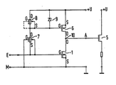
- the electronic switch consists of two MOSFETs 1 and 6, whose drain-source paths are connected in series. If the electronic switch is to switch a positive voltage + U, the first MOSFET 1 is an n-channel FET. The second MOSFET 6 is then a p-channel FET. If a negative voltage is to be switched, the FET 1 is a p-channel and the FET 6 is an n-channel FET. The FET 1 and 6 are connected on the drain side, the connection point 10 is connected to the output terminal A. The gate connection of the FET 1 is connected to the first input terminal E. It is also connected to the source connection of a deposition FET 7, the gate electrode of which is connected to the second input terminal M or ground.
- the drain connection of the FET 7 is connected via a resistor 8 to the supply voltage + U.
- the resistor 8 can, as shown in dashed lines, also be a further depletion FET, the gate connection of which is short-circuited to the source connection. This transistor then acts like a current squeeze with an infinitely high internal resistance.
- Depletion FET 7 and 8 have n-type channels. If a negative voltage is to be switched, depletion FET with p-channel should be used.
- FET 1 If a signal with the level H of z. B. +5 V, FET 1 is turned on and output A is at ground potential.
- the FET 7 receives a negative gate bias and is blocked. This means that there is high potential at the drain connection of the FET 7 and at the gate connection of the FET 6, as a result of which the FET 6 is blocked. The electronic switch is thus blocked, neither load current flows to the consumer 5 nor a cross current through the resistor 8 and the FET 7.
- the FET 1 If a signal with the level L of z. B. 0 V, the FET 1 is blocked and the depletion FET 7 receives the gate-source voltage 0 V. It is then switched on and a current can flow through the resistor 8 and the FET 7. A potential is then established at the gate connection of the p-channel FET 6, which is determined by the voltage divider ratio between resistor 8 and FET 7. This tension is positive and remains constant. The source connection of the FET 6 is at a constant voltage. The electronic switch can thus switch on very quickly and a capacitive load on the output terminal A, e.g. B. the gate capacitance of a power FET is charged very quickly.
- the gate-source path of the MOSFET 6 can with respect to voltage in the usual manner, for. B. protected by a Zener diode 9.
Landscapes
- Engineering & Computer Science (AREA)
- Power Engineering (AREA)
- Physics & Mathematics (AREA)
- Computer Hardware Design (AREA)
- Computing Systems (AREA)
- General Engineering & Computer Science (AREA)
- Mathematical Physics (AREA)
- Electronic Switches (AREA)
Claims (1)
Applications Claiming Priority (2)
| Application Number | Priority Date | Filing Date | Title |
|---|---|---|---|
| DE3521090 | 1985-06-12 | ||
| DE3521090 | 1985-06-12 |
Publications (2)
| Publication Number | Publication Date |
|---|---|
| EP0205158A1 EP0205158A1 (fr) | 1986-12-17 |
| EP0205158B1 true EP0205158B1 (fr) | 1990-01-24 |
Family
ID=6273095
Family Applications (1)
| Application Number | Title | Priority Date | Filing Date |
|---|---|---|---|
| EP86107922A Expired - Lifetime EP0205158B1 (fr) | 1985-06-12 | 1986-06-10 | Commutateur électronique |
Country Status (4)
| Country | Link |
|---|---|
| US (1) | US4677325A (fr) |
| EP (1) | EP0205158B1 (fr) |
| JP (1) | JPH0758899B2 (fr) |
| DE (1) | DE3668522D1 (fr) |
Families Citing this family (8)
| Publication number | Priority date | Publication date | Assignee | Title |
|---|---|---|---|---|
| JPH0760997B2 (ja) * | 1986-06-09 | 1995-06-28 | 日本テキサス・インスツルメンツ株式会社 | 高耐圧出力回路 |
| DE59207678D1 (de) * | 1992-06-05 | 1997-01-23 | Siemens Ag | Ansteuerschaltung für einen Leistungs-FET mit sourceseitiger Last |
| US5401973A (en) * | 1992-12-04 | 1995-03-28 | Atomic Energy Of Canada Limited | Industrial material processing electron linear accelerator |
| US5467050A (en) * | 1994-01-04 | 1995-11-14 | Texas Instruments Incorporated | Dynamic biasing circuit for semiconductor device |
| US5537072A (en) * | 1994-06-30 | 1996-07-16 | Sgs-Thomson Microelectronics, Inc. | Charge pump switch circuits |
| JP3228093B2 (ja) * | 1995-06-28 | 2001-11-12 | 富士電機株式会社 | 高耐圧ic |
| GB2335556B (en) | 1998-03-18 | 2002-10-30 | Ericsson Telefon Ab L M | Switch circuit |
| US7400171B1 (en) * | 2005-05-03 | 2008-07-15 | Lattice Semiconductor Corporation | Electronic switch having extended voltage range |
Family Cites Families (7)
| Publication number | Priority date | Publication date | Assignee | Title |
|---|---|---|---|---|
| US952012A (en) * | 1908-11-05 | 1910-03-15 | Frederick Mayer | Wheel. |
| US3823330A (en) * | 1973-01-18 | 1974-07-09 | Inselek Inc | Circuit for shifting and amplifying input voltages |
| UST952012I4 (fr) | 1976-01-20 | 1976-11-02 | ||
| US4064405A (en) * | 1976-11-09 | 1977-12-20 | Westinghouse Electric Corporation | Complementary MOS logic circuit |
| NL7805068A (nl) * | 1978-05-11 | 1979-11-13 | Philips Nv | Drempelschakeling. |
| JPS55136726A (en) * | 1979-04-11 | 1980-10-24 | Nec Corp | High voltage mos inverter and its drive method |
| JPS6079822A (ja) * | 1983-10-07 | 1985-05-07 | Hitachi Ltd | Cmos集積回路装置 |
-
1986
- 1986-06-09 JP JP61133589A patent/JPH0758899B2/ja not_active Expired - Fee Related
- 1986-06-09 US US06/872,354 patent/US4677325A/en not_active Expired - Lifetime
- 1986-06-10 DE DE8686107922T patent/DE3668522D1/de not_active Expired - Lifetime
- 1986-06-10 EP EP86107922A patent/EP0205158B1/fr not_active Expired - Lifetime
Also Published As
| Publication number | Publication date |
|---|---|
| JPH0758899B2 (ja) | 1995-06-21 |
| DE3668522D1 (de) | 1990-03-01 |
| JPS61285820A (ja) | 1986-12-16 |
| EP0205158A1 (fr) | 1986-12-17 |
| US4677325A (en) | 1987-06-30 |
Similar Documents
| Publication | Publication Date | Title |
|---|---|---|
| EP0747713B1 (fr) | Circuit capteur de courant de charge d'un composant semi-conducteur de puissance avec charge soit à la borne de source ou soit à la borne de drain | |
| DE2411839C3 (de) | Integrierte Feldeffekttransistor-Schaltung | |
| DE3750463T2 (de) | Schalteinrichtung mit dynamischer Hysterese. | |
| DE68912617T2 (de) | Spannungsseitige MOS-Treiberschaltung. | |
| DE2659207B2 (de) | In einem integrierten MOSFET-Schaltkreis ausgebildete Verzögerungsstufe | |
| EP0352659B1 (fr) | Circuit pour déterminer des court-circuits dans une charge en série avec un FET | |
| EP0304951B1 (fr) | Coupleur optique | |
| DE19638087C2 (de) | CMOS-Komparator | |
| DE69216663T2 (de) | Schaltkreis | |
| DE2356974A1 (de) | Aus feldeffekttransistoren aufgebaute gegentakt-treiberschaltung fuer digitale anwendungen | |
| DE69206335T2 (de) | Unter niedriger Spannung betriebener Stromspiegel. | |
| EP0205158B1 (fr) | Commutateur électronique | |
| EP0794619A2 (fr) | Montage pour le commande d'un transistor à effet de champ à charge connectée à la source | |
| EP0582125B1 (fr) | Circuit de commande pour un MOSFET de puissance ayant une charge connectée à la source | |
| DE4444623A1 (de) | Schaltungsanordnung zur Laststromregelung eines Leistungs-MOSFET | |
| DE2421988C2 (de) | Analogspannungsschalter | |
| DE2556683B2 (de) | Negativ-Widerstandsnetzwerk | |
| DE2061943C3 (de) | Differenzverstärker | |
| DE2301855C3 (de) | Schaltungsanordnung mit Feldeffekttransistoren zur Pegelanpassung | |
| DE4403201C2 (de) | Ansteuerschaltung für ein MOS-Halbleiterbauelement mit sourceseitiger Last | |
| EP0544143B1 (fr) | Circuit comparateur intégré | |
| EP0365706B1 (fr) | Etage de sortie de puissance avec une charge | |
| DE69023358T2 (de) | Logische Schaltung. | |
| EP0753754A2 (fr) | Circuit comparateur intégré | |
| DE3124891C2 (de) | Transistorschaltstufe |
Legal Events
| Date | Code | Title | Description |
|---|---|---|---|
| PUAI | Public reference made under article 153(3) epc to a published international application that has entered the european phase |
Free format text: ORIGINAL CODE: 0009012 |
|
| AK | Designated contracting states |
Kind code of ref document: A1 Designated state(s): DE FR GB IT |
|
| 17P | Request for examination filed |
Effective date: 19870127 |
|
| 17Q | First examination report despatched |
Effective date: 19881129 |
|
| GRAA | (expected) grant |
Free format text: ORIGINAL CODE: 0009210 |
|
| AK | Designated contracting states |
Kind code of ref document: B1 Designated state(s): DE FR GB IT |
|
| REF | Corresponds to: |
Ref document number: 3668522 Country of ref document: DE Date of ref document: 19900301 |
|
| ET | Fr: translation filed | ||
| ITF | It: translation for a ep patent filed | ||
| GBT | Gb: translation of ep patent filed (gb section 77(6)(a)/1977) | ||
| PLBE | No opposition filed within time limit |
Free format text: ORIGINAL CODE: 0009261 |
|
| STAA | Information on the status of an ep patent application or granted ep patent |
Free format text: STATUS: NO OPPOSITION FILED WITHIN TIME LIMIT |
|
| 26N | No opposition filed | ||
| ITTA | It: last paid annual fee | ||
| PGFP | Annual fee paid to national office [announced via postgrant information from national office to epo] |
Ref country code: DE Payment date: 20010823 Year of fee payment: 16 |
|
| REG | Reference to a national code |
Ref country code: GB Ref legal event code: IF02 |
|
| PGFP | Annual fee paid to national office [announced via postgrant information from national office to epo] |
Ref country code: GB Payment date: 20020610 Year of fee payment: 17 |
|
| PGFP | Annual fee paid to national office [announced via postgrant information from national office to epo] |
Ref country code: FR Payment date: 20020625 Year of fee payment: 17 |
|
| PG25 | Lapsed in a contracting state [announced via postgrant information from national office to epo] |
Ref country code: DE Free format text: LAPSE BECAUSE OF NON-PAYMENT OF DUE FEES Effective date: 20030101 |
|
| PG25 | Lapsed in a contracting state [announced via postgrant information from national office to epo] |
Ref country code: GB Free format text: LAPSE BECAUSE OF NON-PAYMENT OF DUE FEES Effective date: 20030610 |
|
| GBPC | Gb: european patent ceased through non-payment of renewal fee |
Effective date: 20030610 |
|
| PG25 | Lapsed in a contracting state [announced via postgrant information from national office to epo] |
Ref country code: FR Free format text: LAPSE BECAUSE OF NON-PAYMENT OF DUE FEES Effective date: 20040227 |
|
| REG | Reference to a national code |
Ref country code: FR Ref legal event code: ST |
|
| PG25 | Lapsed in a contracting state [announced via postgrant information from national office to epo] |
Ref country code: IT Free format text: LAPSE BECAUSE OF NON-PAYMENT OF DUE FEES;WARNING: LAPSES OF ITALIAN PATENTS WITH EFFECTIVE DATE BEFORE 2007 MAY HAVE OCCURRED AT ANY TIME BEFORE 2007. THE CORRECT EFFECTIVE DATE MAY BE DIFFERENT FROM THE ONE RECORDED. Effective date: 20050610 |