EP0205164A2 - Structure d'un dispositif semi-conducteur - Google Patents
Structure d'un dispositif semi-conducteur Download PDFInfo
- Publication number
- EP0205164A2 EP0205164A2 EP86107956A EP86107956A EP0205164A2 EP 0205164 A2 EP0205164 A2 EP 0205164A2 EP 86107956 A EP86107956 A EP 86107956A EP 86107956 A EP86107956 A EP 86107956A EP 0205164 A2 EP0205164 A2 EP 0205164A2
- Authority
- EP
- European Patent Office
- Prior art keywords
- epitaxial region
- gallium arsenide
- layer
- inp
- semiconductor
- Prior art date
- Legal status (The legal status is an assumption and is not a legal conclusion. Google has not performed a legal analysis and makes no representation as to the accuracy of the status listed.)
- Granted
Links
Images

Classifications
-
- H—ELECTRICITY
- H10—SEMICONDUCTOR DEVICES; ELECTRIC SOLID-STATE DEVICES NOT OTHERWISE PROVIDED FOR
- H10D—INORGANIC ELECTRIC SEMICONDUCTOR DEVICES
- H10D62/00—Semiconductor bodies, or regions thereof, of devices having potential barriers
- H10D62/80—Semiconductor bodies, or regions thereof, of devices having potential barriers characterised by the materials
- H10D62/85—Semiconductor bodies, or regions thereof, of devices having potential barriers characterised by the materials being Group III-V materials, e.g. GaAs
- H10D62/852—Semiconductor bodies, or regions thereof, of devices having potential barriers characterised by the materials being Group III-V materials, e.g. GaAs being Group III-V materials comprising three or more elements, e.g. AlGaN or InAsSbP
-
- H—ELECTRICITY
- H10—SEMICONDUCTOR DEVICES; ELECTRIC SOLID-STATE DEVICES NOT OTHERWISE PROVIDED FOR
- H10D—INORGANIC ELECTRIC SEMICONDUCTOR DEVICES
- H10D30/00—Field-effect transistors [FET]
- H10D30/60—Insulated-gate field-effect transistors [IGFET]
- H10D30/67—Thin-film transistors [TFT]
- H10D30/6729—Thin-film transistors [TFT] characterised by the electrodes
- H10D30/6737—Thin-film transistors [TFT] characterised by the electrodes characterised by the electrode materials
- H10D30/6738—Schottky barrier electrodes
-
- H—ELECTRICITY
- H10—SEMICONDUCTOR DEVICES; ELECTRIC SOLID-STATE DEVICES NOT OTHERWISE PROVIDED FOR
- H10D—INORGANIC ELECTRIC SEMICONDUCTOR DEVICES
- H10D30/00—Field-effect transistors [FET]
- H10D30/60—Insulated-gate field-effect transistors [IGFET]
- H10D30/67—Thin-film transistors [TFT]
- H10D30/674—Thin-film transistors [TFT] characterised by the active materials
- H10D30/675—Group III-V materials, Group II-VI materials, Group IV-VI materials, selenium or tellurium
-
- H—ELECTRICITY
- H10—SEMICONDUCTOR DEVICES; ELECTRIC SOLID-STATE DEVICES NOT OTHERWISE PROVIDED FOR
- H10D—INORGANIC ELECTRIC SEMICONDUCTOR DEVICES
- H10D30/00—Field-effect transistors [FET]
- H10D30/80—FETs having rectifying junction gate electrodes
- H10D30/801—FETs having heterojunction gate electrodes
-
- H—ELECTRICITY
- H10—SEMICONDUCTOR DEVICES; ELECTRIC SOLID-STATE DEVICES NOT OTHERWISE PROVIDED FOR
- H10D—INORGANIC ELECTRIC SEMICONDUCTOR DEVICES
- H10D62/00—Semiconductor bodies, or regions thereof, of devices having potential barriers
- H10D62/80—Semiconductor bodies, or regions thereof, of devices having potential barriers characterised by the materials
- H10D62/85—Semiconductor bodies, or regions thereof, of devices having potential barriers characterised by the materials being Group III-V materials, e.g. GaAs
-
- H—ELECTRICITY
- H10—SEMICONDUCTOR DEVICES; ELECTRIC SOLID-STATE DEVICES NOT OTHERWISE PROVIDED FOR
- H10D—INORGANIC ELECTRIC SEMICONDUCTOR DEVICES
- H10D64/00—Electrodes of devices having potential barriers
- H10D64/60—Electrodes characterised by their materials
- H10D64/602—Heterojunction gate electrodes for FETs
-
- H—ELECTRICITY
- H10—SEMICONDUCTOR DEVICES; ELECTRIC SOLID-STATE DEVICES NOT OTHERWISE PROVIDED FOR
- H10D—INORGANIC ELECTRIC SEMICONDUCTOR DEVICES
- H10D64/00—Electrodes of devices having potential barriers
- H10D64/60—Electrodes characterised by their materials
- H10D64/64—Electrodes comprising a Schottky barrier to a semiconductor
Definitions
- the invention is a semiconductor device, especially applicable for use as a field effect transistor.
- Optical communication technology provides an illustrative example.
- Optical communication has been developing at a rapid rate during the last few years.
- High sensitivity in receivers is desirable because it increases the distance between repeaters and reduces the number of repeaters in a particular communication system.
- Also of importance in optical communication systems is high speed amplifiers which permit high bit rates to be transmitted.
- High speed amplifier systems are also of use in other types of circuits including logic circuits, memory circuits, analog switching, high-input-impedance amplifiers, integrated circuits, etc. -
- indium gallium arsenide and related compounds such as indium gallium arsenide phosphide. This is due to the high mobility and peak electron velocity exhibited by the III-V compound semiconductors. A particular difficulty is in fabricating suitable devices to take advantage of these properties.
- the low barrier heights impose a limitation on the usefulness of Schottky barrier gates for MESFETS with indium gallium arsenide channel layers.
- Various corrective measures can be "used to improve the barrier height characteristics, but a reliable process to produce such devices with reproducible characteristics has not been found.
- a possible approach to this problem is to interpose a thin layer of insulator material or wide band-gap material between metal and channel layer to produce the required barrier height for the control gate.
- Attempts to use a thin layer of gallium arsenide as the barrier material resulted in unacceptably high reverse bias currents (see for example C. Y. Chen et al, IEEE Electron Device Letters, Vol. EDL-6, No. 1, January 1985.
- the invention is a semiconductor device with a channel layer comprising indium phosphide or a III-V semiconductor compound lattice-matched to indium phosphide in which gallium arsenide is used as the barrier material.
- barrier layer thicknesses of greater than 70 (nm) but preferred thicknesses are greater than 80, 100 or even 150 (nm). Thicknesses greater than 300-400 (nm) still yield excellent results but are not significantly better than 150 (nm) and are wasteful of material and processing time.
- Typical structures have indium gallium arsenide as the channel material and indium phosphide as the substrate material.
- Devices made in accordance with the invention have high speeds, high transconductance and are suitable for integration with optical indium phosphide devices (e.g., photodetectors, lasers, etc.).
- the invention is based on the discovery that gallium arsenide layers in a certain thickness range, when deposited on a mismatched layer such as InP or Ga 0.47 In 0.53 As, can yield very low gate leakage currents.
- Such layers are useful in a variety of semiconductor structures. These GaAs layers form Schottky barriers with reasonable barrier heights and low reverse-bias leakage currents.
- Such barrier structures are useful in a variety of semiconductor structures, particularly where the basic layer exhibits only low Schottky barrier heights.
- the substrate material is indium phosphide and the channel material is indium phosphide or a semiconductor lattice-matched to indium phosphide (e.g., indium gallium arsenide with approximate composition In 0.53 Ga 0.47 As or indium aluminum arsenide with approximate composition In 0.52 Al 0.48 As).
- the gallium arsenide layers produce increased Schottky barrier heights which reduces the reverse bias current.
- the invention involves use of gallium arsenide in a certain thickness range as a lattice-mismatched layer on indium gallium arsenide to produce a Schottky barrier with reasonable height.
- the preferred channel material is indium gallium arsenide, particularly the composition of indium gallium arsenide that is lattice-matched to indium phosphide.
- indium gallium arsenide is an important channel material: first, it has high low- field electron mobility, and, second, it can be lattice-matched to indium phosphide useful for a variety of long-.wavelength lightwave integrated circuits. Particularly useful are integrated detector circuits for lightwave receivers and laser driver circuits as well as arrays of FET circuits for fast memories and logic circuits.
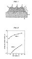
- FIG. 1 A typical FET semiconductor structure 10 using the gallium arsenide layer is shown in FIG. 1.
- the structure is grown on a (100) oriented semi-insulating (usually iron-doped) indium phosphide substrate 11.
- Epitaxial layers are typically grown on this substrate by molecular beam epitaxy (MBE).
- MBE molecular beam epitaxy
- the active device layers consist of: first, a 60 nm thick undoped Ga 0.47 In 0.53 As semi-insulating buffer layer 12; second, a 40 nm thick n-Ga 0.47 In 0.53 As layer 13 doped with silicon to a concentration of 8x10 16 atoms cm-3, a 96 nm thick n-GaAs layer 14 doped with silicon to a concentration of about 10 16 atoms cm 3 and a n + GaAs layer 15 with thickness of about 34 nm and silicon doping concentration of about 10 18 atoms cm - 3 .
- FIG. 2 shows the typical reverse gate leakage currents of both samples.
- Sample 1 has a thin GaAs layer of about 58 nm;
- Sample 2 has a thick GaAs layer of about 130 nm. It is clear that the devices made on a thick GaAs layer have a leakage current at least two orders of magnitude smaller than those of the thin layered sample.
- Sample 1 has a leakage current of 200 pA at 1 V bias while Sample 2 has a leakage current of only 480 nA.
- the major cause for the reduced leakage current in the thick sample is believed to be the reduction in dislocation densities at the surface where Schottky barriers are formed.
- currents can leak through dislocations. It is believed that further reduction in leakage currents can be achieved by improving crystal growth.
- the integrated circuit structure is made on a substrate of semi-insulating InP 31.
- the confinement layers 32 and 34 surround the active layer 33 of a buried heterostructure laser typically made of.InGaAsP with composition which lattice-matches to InP and emits at the desired frequency.
- An insulating layer 35 is used to confine the current to a specific area and a metal contact layer 36 is used as the metal contact to the laser.
- the laser is driven by a FET circuit consisting of a channel layer 37 (usually InGaAs lattice-matched to InP), a drain contact 38 and source contact 39.
- the gate electrode 40 is formed on a GaAs layer 41.
Landscapes
- Junction Field-Effect Transistors (AREA)
- Semiconductor Lasers (AREA)
Applications Claiming Priority (2)
| Application Number | Priority Date | Filing Date | Title |
|---|---|---|---|
| US06/745,294 US4745447A (en) | 1985-06-14 | 1985-06-14 | Gallium arsenide on gallium indium arsenide Schottky barrier device |
| US745294 | 1985-06-14 |
Publications (3)
| Publication Number | Publication Date |
|---|---|
| EP0205164A2 true EP0205164A2 (fr) | 1986-12-17 |
| EP0205164A3 EP0205164A3 (en) | 1987-12-23 |
| EP0205164B1 EP0205164B1 (fr) | 1990-05-16 |
Family
ID=24996087
Family Applications (1)
| Application Number | Title | Priority Date | Filing Date |
|---|---|---|---|
| EP86107956A Expired EP0205164B1 (fr) | 1985-06-14 | 1986-06-11 | Structure d'un dispositif semi-conducteur |
Country Status (5)
| Country | Link |
|---|---|
| US (1) | US4745447A (fr) |
| EP (1) | EP0205164B1 (fr) |
| JP (1) | JP2636840B2 (fr) |
| CA (1) | CA1240406A (fr) |
| DE (1) | DE3671328D1 (fr) |
Cited By (3)
| Publication number | Priority date | Publication date | Assignee | Title |
|---|---|---|---|---|
| EP0497305A3 (en) * | 1991-01-31 | 1992-12-16 | Texas Instruments Incorporated | Gsas fet with resistive algaas |
| EP0523731A3 (fr) * | 1991-07-17 | 1995-05-17 | Sumitomo Electric Industries | |
| EP0851510A3 (fr) * | 1996-12-25 | 1999-02-24 | Murata Manufacturing Co., Ltd. | Transistor à effet de champ |
Families Citing this family (7)
| Publication number | Priority date | Publication date | Assignee | Title |
|---|---|---|---|---|
| JPS63114176A (ja) * | 1986-10-31 | 1988-05-19 | Fujitsu Ltd | 高速電界効果半導体装置 |
| JPS63144580A (ja) * | 1986-12-09 | 1988-06-16 | Nec Corp | 電界効果トランジスタ |
| JPS63276267A (ja) * | 1987-05-08 | 1988-11-14 | Fujitsu Ltd | 半導体装置の製造方法 |
| US5091759A (en) * | 1989-10-30 | 1992-02-25 | Texas Instruments Incorporated | Heterostructure field effect transistor |
| US5298441A (en) * | 1991-06-03 | 1994-03-29 | Motorola, Inc. | Method of making high transconductance heterostructure field effect transistor |
| US6097748A (en) * | 1998-05-18 | 2000-08-01 | Motorola, Inc. | Vertical cavity surface emitting laser semiconductor chip with integrated drivers and photodetectors and method of fabrication |
| US20190145926A1 (en) * | 2016-04-29 | 2019-05-16 | Stc. Unm | Wafer level gate modulation enhanced detectors |
Family Cites Families (10)
| Publication number | Priority date | Publication date | Assignee | Title |
|---|---|---|---|---|
| US3218205A (en) * | 1962-07-13 | 1965-11-16 | Monsanto Co | Use of hydrogen halide and hydrogen in separate streams as carrier gases in vapor deposition of iii-v compounds |
| FR2386903A1 (fr) * | 1977-04-08 | 1978-11-03 | Thomson Csf | Transistor a effet de champ sur support a grande bande interdite |
| GB2012480A (en) * | 1978-01-12 | 1979-07-25 | Plessey Co Ltd | Heterostructure field effect transistors |
| FR2465318A1 (fr) * | 1979-09-10 | 1981-03-20 | Thomson Csf | Transistor a effet de champ a frequence de coupure elevee |
| US4360246A (en) * | 1980-05-23 | 1982-11-23 | Hughes Aircraft Company | Integrated waveguide and FET detector |
| JPS58147166A (ja) * | 1982-02-26 | 1983-09-01 | Fujitsu Ltd | 半導体装置 |
| JPS59222988A (ja) * | 1983-06-01 | 1984-12-14 | Matsushita Electric Ind Co Ltd | 化合物半導体素子およびその製造方法 |
| JPS59222986A (ja) * | 1983-06-01 | 1984-12-14 | Matsushita Electric Ind Co Ltd | 化合物半導体素子の製造方法 |
| JPS609174A (ja) * | 1983-06-29 | 1985-01-18 | Fujitsu Ltd | 半導体装置 |
| JPS61225874A (ja) * | 1985-03-29 | 1986-10-07 | Sumitomo Electric Ind Ltd | 電界効果トランジスタ |
-
1985
- 1985-06-14 US US06/745,294 patent/US4745447A/en not_active Expired - Lifetime
-
1986
- 1986-05-28 CA CA000510185A patent/CA1240406A/fr not_active Expired
- 1986-06-11 DE DE8686107956T patent/DE3671328D1/de not_active Expired - Fee Related
- 1986-06-11 EP EP86107956A patent/EP0205164B1/fr not_active Expired
- 1986-06-13 JP JP61136381A patent/JP2636840B2/ja not_active Expired - Lifetime
Cited By (5)
| Publication number | Priority date | Publication date | Assignee | Title |
|---|---|---|---|---|
| EP0497305A3 (en) * | 1991-01-31 | 1992-12-16 | Texas Instruments Incorporated | Gsas fet with resistive algaas |
| EP0523731A3 (fr) * | 1991-07-17 | 1995-05-17 | Sumitomo Electric Industries | |
| EP0851510A3 (fr) * | 1996-12-25 | 1999-02-24 | Murata Manufacturing Co., Ltd. | Transistor à effet de champ |
| US6008509A (en) * | 1996-12-25 | 1999-12-28 | Murata Manufacturing Co., Ltd. | Field effect transistor |
| KR100548047B1 (ko) * | 1996-12-25 | 2007-11-09 | 가부시키가이샤 무라타 세이사쿠쇼 | 전계효과트랜지스터 |
Also Published As
| Publication number | Publication date |
|---|---|
| CA1240406A (fr) | 1988-08-09 |
| DE3671328D1 (de) | 1990-06-21 |
| JP2636840B2 (ja) | 1997-07-30 |
| US4745447A (en) | 1988-05-17 |
| JPS61290776A (ja) | 1986-12-20 |
| EP0205164B1 (fr) | 1990-05-16 |
| EP0205164A3 (en) | 1987-12-23 |
Similar Documents
| Publication | Publication Date | Title |
|---|---|---|
| US4829347A (en) | Process for making indium gallium arsenide devices | |
| US4827320A (en) | Semiconductor device with strained InGaAs layer | |
| US5705827A (en) | Tunnel transistor and method of manufacturing same | |
| US5495115A (en) | Semiconductor crystalline laminate structure, forming method of the same, and semiconductor device employing the same | |
| US5091759A (en) | Heterostructure field effect transistor | |
| Matsumoto et al. | n+-GaAs/undoped GaAlAs/undoped GaAs field-effect transistor | |
| EP0460793B1 (fr) | Transistor à effet de champ à hétérojonction avec un canal enseveli | |
| EP0051271A1 (fr) | Dispositif semiconducteur à hétérojonctions | |
| JP2914049B2 (ja) | ヘテロ接合を有する化合物半導体基板およびそれを用いた電界効果トランジスタ | |
| EP0205164B1 (fr) | Structure d'un dispositif semi-conducteur | |
| US4829346A (en) | Field-effect transistor and the same associated with an optical semiconductor device | |
| US4942438A (en) | Compound semiconductor field-effect transistor | |
| US20040178422A1 (en) | Heterostructure field effect transistor | |
| US4600932A (en) | Enhanced mobility buried channel transistor structure | |
| US5024967A (en) | Doping procedures for semiconductor devices | |
| US5466955A (en) | Field effect transistor having an improved transistor characteristic | |
| US5751029A (en) | Field-effect semiconductor device having heterojunction | |
| JP3421306B2 (ja) | 化合物半導体装置 | |
| US5311045A (en) | Field effect devices with ultra-short gates | |
| US5408111A (en) | Field-effect transistor having a double pulse-doped structure | |
| JPS6242569A (ja) | 電界効果型トランジスタ | |
| JP3414262B2 (ja) | 化合物半導体エピタキシャルウェハ及び化合物半導体装置 | |
| JPH09237889A (ja) | 半導体結晶積層体及びそれを用いた半導体装置 | |
| Vokes et al. | Novel microwave GaAs field-effect transistors | |
| Prost et al. | High speed, high gain InP-based heterostructure FETs with high breakdown voltage and low leakage |
Legal Events
| Date | Code | Title | Description |
|---|---|---|---|
| PUAI | Public reference made under article 153(3) epc to a published international application that has entered the european phase |
Free format text: ORIGINAL CODE: 0009012 |
|
| AK | Designated contracting states |
Kind code of ref document: A2 Designated state(s): DE FR GB NL |
|
| PUAL | Search report despatched |
Free format text: ORIGINAL CODE: 0009013 |
|
| AK | Designated contracting states |
Kind code of ref document: A3 Designated state(s): DE FR GB NL |
|
| 17P | Request for examination filed |
Effective date: 19880620 |
|
| 17Q | First examination report despatched |
Effective date: 19880822 |
|
| GRAA | (expected) grant |
Free format text: ORIGINAL CODE: 0009210 |
|
| AK | Designated contracting states |
Kind code of ref document: B1 Designated state(s): DE FR GB NL |
|
| REF | Corresponds to: |
Ref document number: 3671328 Country of ref document: DE Date of ref document: 19900621 |
|
| ET | Fr: translation filed | ||
| PLBE | No opposition filed within time limit |
Free format text: ORIGINAL CODE: 0009261 |
|
| STAA | Information on the status of an ep patent application or granted ep patent |
Free format text: STATUS: NO OPPOSITION FILED WITHIN TIME LIMIT |
|
| 26N | No opposition filed | ||
| PGFP | Annual fee paid to national office [announced via postgrant information from national office to epo] |
Ref country code: GB Payment date: 20010525 Year of fee payment: 16 Ref country code: FR Payment date: 20010525 Year of fee payment: 16 |
|
| PGFP | Annual fee paid to national office [announced via postgrant information from national office to epo] |
Ref country code: NL Payment date: 20010529 Year of fee payment: 16 |
|
| PGFP | Annual fee paid to national office [announced via postgrant information from national office to epo] |
Ref country code: DE Payment date: 20010629 Year of fee payment: 16 |
|
| REG | Reference to a national code |
Ref country code: GB Ref legal event code: IF02 |
|
| PG25 | Lapsed in a contracting state [announced via postgrant information from national office to epo] |
Ref country code: GB Free format text: LAPSE BECAUSE OF NON-PAYMENT OF DUE FEES Effective date: 20020611 |
|
| PG25 | Lapsed in a contracting state [announced via postgrant information from national office to epo] |
Ref country code: NL Free format text: LAPSE BECAUSE OF NON-PAYMENT OF DUE FEES Effective date: 20030101 Ref country code: DE Free format text: LAPSE BECAUSE OF NON-PAYMENT OF DUE FEES Effective date: 20030101 |
|
| GBPC | Gb: european patent ceased through non-payment of renewal fee |
Effective date: 20020611 |
|
| PG25 | Lapsed in a contracting state [announced via postgrant information from national office to epo] |
Ref country code: FR Free format text: LAPSE BECAUSE OF NON-PAYMENT OF DUE FEES Effective date: 20030228 |
|
| NLV4 | Nl: lapsed or anulled due to non-payment of the annual fee |
Effective date: 20030101 |
|
| REG | Reference to a national code |
Ref country code: FR Ref legal event code: ST |