EP0205185A2 - Objectif comportant un spectromètre en technique de mesure par faisceau d'électrons - Google Patents
Objectif comportant un spectromètre en technique de mesure par faisceau d'électrons Download PDFInfo
- Publication number
- EP0205185A2 EP0205185A2 EP86108126A EP86108126A EP0205185A2 EP 0205185 A2 EP0205185 A2 EP 0205185A2 EP 86108126 A EP86108126 A EP 86108126A EP 86108126 A EP86108126 A EP 86108126A EP 0205185 A2 EP0205185 A2 EP 0205185A2
- Authority
- EP
- European Patent Office
- Prior art keywords
- spectrometer
- secondary electrons
- lens
- sample
- objective lens
- Prior art date
- Legal status (The legal status is an assumption and is not a legal conclusion. Google has not performed a legal analysis and makes no representation as to the accuracy of the status listed.)
- Granted
Links
- 238000010894 electron beam technology Methods 0.000 title claims abstract description 11
- 238000000034 method Methods 0.000 title 1
- 230000003287 optical effect Effects 0.000 claims abstract description 17
- 230000005684 electric field Effects 0.000 claims description 8
- 230000001960 triggered effect Effects 0.000 claims description 5
- 238000007654 immersion Methods 0.000 claims description 3
- 238000005259 measurement Methods 0.000 claims description 3
- 230000001133 acceleration Effects 0.000 claims description 2
- 238000005516 engineering process Methods 0.000 claims description 2
- 238000001514 detection method Methods 0.000 claims 1
- 239000000523 sample Substances 0.000 abstract description 22
- 230000000694 effects Effects 0.000 abstract description 6
- 230000002349 favourable effect Effects 0.000 abstract description 3
- 239000008186 active pharmaceutical agent Substances 0.000 description 6
- 230000003993 interaction Effects 0.000 description 3
- 230000008901 benefit Effects 0.000 description 2
- 238000011161 development Methods 0.000 description 2
- 230000018109 developmental process Effects 0.000 description 2
- 230000009467 reduction Effects 0.000 description 2
- 239000007787 solid Substances 0.000 description 2
- 239000000126 substance Substances 0.000 description 2
- 230000002411 adverse Effects 0.000 description 1
- 230000004075 alteration Effects 0.000 description 1
- 239000004020 conductor Substances 0.000 description 1
- 238000010276 construction Methods 0.000 description 1
- 230000001419 dependent effect Effects 0.000 description 1
- 230000006872 improvement Effects 0.000 description 1
- 238000011835 investigation Methods 0.000 description 1
- 230000005855 radiation Effects 0.000 description 1
- 238000007493 shaping process Methods 0.000 description 1
Images

Classifications
-
- H—ELECTRICITY
- H01—ELECTRIC ELEMENTS
- H01J—ELECTRIC DISCHARGE TUBES OR DISCHARGE LAMPS
- H01J49/00—Particle spectrometers or separator tubes
- H01J49/02—Details
- H01J49/06—Electron- or ion-optical arrangements
-
- G—PHYSICS
- G01—MEASURING; TESTING
- G01R—MEASURING ELECTRIC VARIABLES; MEASURING MAGNETIC VARIABLES
- G01R31/00—Arrangements for testing electric properties; Arrangements for locating electric faults; Arrangements for electrical testing characterised by what is being tested not provided for elsewhere
- G01R31/28—Testing of electronic circuits, e.g. by signal tracer
- G01R31/302—Contactless testing
- G01R31/305—Contactless testing using electron beams
-
- H—ELECTRICITY
- H01—ELECTRIC ELEMENTS
- H01J—ELECTRIC DISCHARGE TUBES OR DISCHARGE LAMPS
- H01J37/00—Discharge tubes with provision for introducing objects or material to be exposed to the discharge, e.g. for the purpose of examination or processing thereof
- H01J37/02—Details
- H01J37/04—Arrangements of electrodes and associated parts for generating or controlling the discharge, e.g. electron-optical arrangement or ion-optical arrangement
- H01J37/147—Arrangements for directing or deflecting the discharge along a desired path
- H01J37/1472—Deflecting along given lines
- H01J37/1474—Scanning means
-
- H—ELECTRICITY
- H01—ELECTRIC ELEMENTS
- H01J—ELECTRIC DISCHARGE TUBES OR DISCHARGE LAMPS
- H01J37/00—Discharge tubes with provision for introducing objects or material to be exposed to the discharge, e.g. for the purpose of examination or processing thereof
- H01J37/26—Electron or ion microscopes; Electron or ion diffraction tubes
- H01J37/266—Measurement of magnetic or electric fields in the object; Lorentzmicroscopy
- H01J37/268—Measurement of magnetic or electric fields in the object; Lorentzmicroscopy with scanning beams
-
- H—ELECTRICITY
- H01—ELECTRIC ELEMENTS
- H01J—ELECTRIC DISCHARGE TUBES OR DISCHARGE LAMPS
- H01J49/00—Particle spectrometers or separator tubes
- H01J49/44—Energy spectrometers, e.g. alpha-, beta-spectrometers
- H01J49/46—Static spectrometers
- H01J49/48—Static spectrometers using electrostatic analysers, e.g. cylindrical sector, Wien filter
- H01J49/488—Static spectrometers using electrostatic analysers, e.g. cylindrical sector, Wien filter with retarding grids
Definitions
- the invention relates to a spectrometer lens for electron beam measurement technology according to the preamble of claim 1.
- This known arrangement is a magnetic objective lens with a short focal length with an integrated parallel plate analyzer and an electrode arranged above the objective lens for deflecting the secondary electrons in the direction of a detector.
- the diameter of the electron probe on the sample can be significantly reduced in comparison with conventional arrangements in an electron beam measuring device equipped with the known spectrometer objective, the spatial resolution of these devices remains limited. The reason for this is the Coulomb repulsion of the electrons in the beam path between the electron source and the sample, which counteracts a focusing of the electron beam.
- the invention has for its object to provide a spectrometer lens of the type mentioned, with which the electron-optical beam path between the beam generator and the sample is shortened and thus the influence of the Boersch effect on the probe diameter can be significantly reduced.
- the advantage that can be achieved with the invention is, in particular, that the spatial and potential resolution of an electron beam measuring device can be significantly increased even with high probe currents.
- the primary electrons are deflected within the spectrometer objective, so that the space for the two-stage deflection systems between the condenser lens and the objective lens used in conventional arrangements can be saved.
- the extremely short overall length of the electron beam measuring device that can be achieved in this way in turn has a favorable effect on the influence of the lateral Boersch effect on the probe diameter that increases with the length of the beam path.
- Claims 2 to 7 are directed to preferred refinements and developments of the invention.
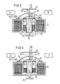
- the exemplary embodiment of a spectrometer objective according to the invention shown in FIGS. 1 and 2 consists of a short focal length, largely asymmetrical objective lens OL with an integrated electrostatic counterfield spectrometer and a single-stage magnetic deflection system DS arranged symmetrically to the optical axis OA within the magnetic lens OL.
- This overall system forms an electron-optical unit with which both the primary electrons PE generated, for example, in a high-current electron source Q and the secondary electrons SE triggered on a sample PR are focused into a point lying on the optical axis OA.
- the electron source Q or the intermediate image ZP of the source Q reduced by condenser lenses KL is reduced again with the aid of the spectrometer lens as part of the beam-shaping system onto a sample PR arranged in the immediate vicinity of the rear focal plane of the objective lens OL.
- the use of short focal length objective lenses offers a number of advantages. As a result of the. Focal lengths between 3 and 12 mm achievable high lens reduction, the required system reduction can be achieved by a short beam path. However, a short beam path is of crucial importance, especially for reducing the adverse effects of the electron-electron interaction on the probe diameter.
- objective lenses with a short focal length are distinguished in particular by smaller axial color and aperture errors which increase with the focal length.
- these secondary electrons SE are in the electric field of a grid electrode G1 lying at a high positive potential V e between 1 and 5 kV aspirated and accelerated in the direction of the optical axis OA.
- the secondary electrons SE pass through this flat grid electrode G1 with high energies and are focused in the magnetic field of the objective lens OL into a point ZS located on the optical axis OA within the spectrometer objective.
- the position of this focusing point ZS is determined by the level of the voltage V e of the grid electrode G1 and the strength of the magnetic field between the pole pieces of the objective lens OL, which is dependent on the primary electron energy.
- the disadvantageous influence of the Boersch effect on the probe diameter is also reduced in this part of the beam path.
- the opening and color errors of the magnetic lens OL are reduced as a result of the superimposition of the focusing magnetic field of the objective lens and the electrical field of the suction electrode G1 which brakes the primary electrons PE.
- the braking and energy analysis of the secondary electrons SE takes place directly above the objective lens OL in a preferably spherically symmetrical electrical opposing field, which is built up in the spatial area between two spherically symmetrical network electrodes K1 and K2 which have different potentials V E and V G.
- Such electrode arrangements are known, for example, from US Pat. No. 4,464,571.
- the lower, spherically symmetrical network electrode K1 is conductively connected to the suction electrode G1 via a hollow cylinder HZ arranged concentrically to the optical axis OA.
- the potential V a of the upper network electrode K2, which acts as an opposing field grid, is determined by the sample potential and is typically between approximately 0 and minus 20 volts.
- the secondary electron lobe is tilted around the center M of the deflection system DS when the electron probe is rasterized, it is possible to detect the secondary electrons SE emitted in the direction of the axis of symmetry of the lobe with one or more detectors DT arranged symmetrically to the optical axis OA.
- a grating AE lying at a negative potential can also be provided above the spherically symmetrical network electrodes K1 and K2 for deflecting the secondary electrons SE emitted in the direction of the optical axis OA.
- the embodiment of a spectrometer lens according to the invention shown in FIG. 3 consists of a short focal length magnetic objective lens OL with an integrated electrostatic counterfield spectrometer and one within the Magnetic lens OL arranged single-stage deflection system DS.
- the suction and acceleration of the secondary electrons SE takes place in the field of an electrostatic immersion lens, which consists of the spherically symmetrical network electrode K1, the hollow cylinder HZ arranged concentrically to the optical axis OA, and the pole shoes lying at earth potential of the objective lens OL.
- This combination of a magnetic lens with a superimposed electrical immersion lens is distinguished from arrangements with only one magnetic lens by more favorable color error values.
Landscapes
- Chemical & Material Sciences (AREA)
- Analytical Chemistry (AREA)
- Engineering & Computer Science (AREA)
- General Engineering & Computer Science (AREA)
- Physics & Mathematics (AREA)
- General Physics & Mathematics (AREA)
- Analysing Materials By The Use Of Radiation (AREA)
- Electron Tubes For Measurement (AREA)
Applications Claiming Priority (2)
| Application Number | Priority Date | Filing Date | Title |
|---|---|---|---|
| DE3521464 | 1985-06-14 | ||
| DE19853521464 DE3521464A1 (de) | 1985-06-14 | 1985-06-14 | Spektrometer-objektiv fuer die elektronenstrahl-messtechnik |
Publications (3)
| Publication Number | Publication Date |
|---|---|
| EP0205185A2 true EP0205185A2 (fr) | 1986-12-17 |
| EP0205185A3 EP0205185A3 (en) | 1989-01-04 |
| EP0205185B1 EP0205185B1 (fr) | 1991-09-25 |
Family
ID=6273350
Family Applications (1)
| Application Number | Title | Priority Date | Filing Date |
|---|---|---|---|
| EP86108126A Expired - Lifetime EP0205185B1 (fr) | 1985-06-14 | 1986-06-13 | Objectif comportant un spectromètre en technique de mesure par faisceau d'électrons |
Country Status (4)
| Country | Link |
|---|---|
| US (1) | US4808821A (fr) |
| EP (1) | EP0205185B1 (fr) |
| JP (1) | JP2632808B2 (fr) |
| DE (2) | DE3521464A1 (fr) |
Cited By (2)
| Publication number | Priority date | Publication date | Assignee | Title |
|---|---|---|---|---|
| CN102169790A (zh) * | 2011-03-29 | 2011-08-31 | 北京航空航天大学 | 电子显微镜的第一聚光镜 |
| CN102184828A (zh) * | 2011-03-29 | 2011-09-14 | 北京航空航天大学 | 电子显微镜的第二聚光镜 |
Families Citing this family (13)
| Publication number | Priority date | Publication date | Assignee | Title |
|---|---|---|---|---|
| EP0236807A3 (fr) * | 1986-03-07 | 1990-05-16 | Siemens Aktiengesellschaft | Objectif de spectromètre en technique de mesure par faisceau corpusculaire |
| EP0470300B1 (fr) * | 1990-08-09 | 1997-07-02 | Koninklijke Philips Electronics N.V. | Appareil à faisceau d'electrons ayant un champ magnétique de forme monopolaire |
| US5586321A (en) * | 1995-02-21 | 1996-12-17 | Ramot Ltd. | Diffracting token router and applications thereof |
| EP1022766B1 (fr) * | 1998-11-30 | 2004-02-04 | Advantest Corporation | Appareil à faisceau de particules |
| JP2003331770A (ja) * | 2002-05-15 | 2003-11-21 | Seiko Instruments Inc | 電子線装置 |
| JP4316394B2 (ja) * | 2004-01-21 | 2009-08-19 | 株式会社東芝 | 荷電ビーム装置 |
| US7872236B2 (en) * | 2007-01-30 | 2011-01-18 | Hermes Microvision, Inc. | Charged particle detection devices |
| US7759653B2 (en) * | 2008-05-30 | 2010-07-20 | Hermes Microvision, Inc. | Electron beam apparatus |
| US7960697B2 (en) | 2008-10-23 | 2011-06-14 | Hermes-Microvision, Inc. | Electron beam apparatus |
| US7919760B2 (en) * | 2008-12-09 | 2011-04-05 | Hermes-Microvision, Inc. | Operation stage for wafer edge inspection and review |
| US8094924B2 (en) * | 2008-12-15 | 2012-01-10 | Hermes-Microvision, Inc. | E-beam defect review system |
| US8537967B2 (en) * | 2009-09-10 | 2013-09-17 | University Of Washington | Short working distance spectrometer and associated devices, systems, and methods |
| DE102015210893B4 (de) * | 2015-06-15 | 2019-05-09 | Carl Zeiss Microscopy Gmbh | Analyseeinrichtung zur Analyse der Energie geladener Teilchen und Teilchenstrahlgerät mit einer Analyseeinrichtung |
Family Cites Families (5)
| Publication number | Priority date | Publication date | Assignee | Title |
|---|---|---|---|---|
| US3930181A (en) * | 1973-12-28 | 1975-12-30 | Ibm | Lens and deflection unit arrangement for electron beam columns |
| DE3138901A1 (de) * | 1981-09-30 | 1983-04-14 | Siemens AG, 1000 Berlin und 8000 München | Verbessertes gegenfeld-spektrometer fuer die elektronenstrahl-messtechnik |
| JPS58197644A (ja) * | 1982-05-13 | 1983-11-17 | Akashi Seisakusho Co Ltd | 電子顕微鏡およびその類似装置 |
| JPS5923440A (ja) * | 1982-07-29 | 1984-02-06 | Nippon Telegr & Teleph Corp <Ntt> | 荷電粒子ビ−ム用集束偏向装置 |
| DE3236271A1 (de) * | 1982-09-30 | 1984-04-05 | Siemens AG, 1000 Berlin und 8000 München | Spektrometerobjektiv fuer die korpuskularstrahl-messtechnik |
-
1985
- 1985-06-14 DE DE19853521464 patent/DE3521464A1/de not_active Withdrawn
-
1986
- 1986-06-11 JP JP61135877A patent/JP2632808B2/ja not_active Expired - Lifetime
- 1986-06-13 EP EP86108126A patent/EP0205185B1/fr not_active Expired - Lifetime
- 1986-06-13 DE DE8686108126T patent/DE3681634D1/de not_active Expired - Lifetime
- 1986-06-16 US US06/874,498 patent/US4808821A/en not_active Expired - Lifetime
Cited By (4)
| Publication number | Priority date | Publication date | Assignee | Title |
|---|---|---|---|---|
| CN102169790A (zh) * | 2011-03-29 | 2011-08-31 | 北京航空航天大学 | 电子显微镜的第一聚光镜 |
| CN102184828A (zh) * | 2011-03-29 | 2011-09-14 | 北京航空航天大学 | 电子显微镜的第二聚光镜 |
| CN102169790B (zh) * | 2011-03-29 | 2012-07-04 | 北京航空航天大学 | 电子显微镜的第一聚光镜 |
| CN102184828B (zh) * | 2011-03-29 | 2013-02-06 | 北京航空航天大学 | 电子显微镜的第二聚光镜 |
Also Published As
| Publication number | Publication date |
|---|---|
| EP0205185A3 (en) | 1989-01-04 |
| DE3521464A1 (de) | 1986-12-18 |
| JP2632808B2 (ja) | 1997-07-23 |
| JPS61288358A (ja) | 1986-12-18 |
| DE3681634D1 (de) | 1991-10-31 |
| US4808821A (en) | 1989-02-28 |
| EP0205185B1 (fr) | 1991-09-25 |
Similar Documents
| Publication | Publication Date | Title |
|---|---|---|
| EP0205184B1 (fr) | Objectif de faible aberration comportant un spectromètre de haute acceptance en électrons secondaires | |
| EP0281743B1 (fr) | Objectif détecteur pour microscope à balayage | |
| EP0461442B1 (fr) | Appareil à faisceau de particules | |
| EP0333018B1 (fr) | Lentille d'objectif pour la focalisation de particules chargées | |
| EP0267555B1 (fr) | Objectif de spectromètre pour appareils de mesure par faisceau corpusculaire et procédé pour l'examen d'échantillons. | |
| EP0274622B1 (fr) | Assemblage de détecteur avec un objectif muni d'un détecteur pour instruments à rayons corpusculaires | |
| DE19732093B4 (de) | Korpuskularstrahlgerät | |
| US4649316A (en) | Ion beam species filter and blanker | |
| EP0205185B1 (fr) | Objectif comportant un spectromètre en technique de mesure par faisceau d'électrons | |
| EP0218829B1 (fr) | Dispositif détecteur d'électrons secondaires et/ou d'électrons de dispersion en retour dans un appareil à faisceau électronique | |
| DE3590146C2 (fr) | ||
| EP0242602A2 (fr) | Lentille électrostatique et magnétique pour appareils à faisceau corpusculaire | |
| EP0370276B1 (fr) | Dispositif pour détecter des particules chargées secondaires | |
| EP0105439B1 (fr) | Objectif de spectromètre à champs d'objectif et de spectromètre parallèles utilisé en technique de mesure de potentiel | |
| EP0194570A2 (fr) | Microscope corpusculaire à balayage à effet Boersch réduit | |
| EP0236807A2 (fr) | Objectif de spectromètre en technique de mesure par faisceau corpusculaire | |
| EP0348785A2 (fr) | Appareil de mesure par faisceau d'électrons | |
| DE3703028A1 (de) | Rastermikroskop | |
| EP0036618B1 (fr) | Source d'électrons à grande intensité de courant | |
| DE69501533T2 (de) | Partikel-optisches instrument mit einer ablenkeinheit für sekundärelektronen | |
| DE69606515T2 (de) | Elektrostatisch-magnetische Linsenanordnung | |
| EP0086431A2 (fr) | Système générateur de faisceau de particules et méthode d'utilisation | |
| US5089699A (en) | Secondary charged particle analyzing apparatus and secondary charged particle extracting section | |
| DE4236273A1 (en) | Lens for focussing electrons for specimen inspection - has field generated by coils and cone-shaped electrode set into entry section | |
| DE2752933A1 (de) | Elektronenmikroskop |
Legal Events
| Date | Code | Title | Description |
|---|---|---|---|
| PUAI | Public reference made under article 153(3) epc to a published international application that has entered the european phase |
Free format text: ORIGINAL CODE: 0009012 |
|
| AK | Designated contracting states |
Kind code of ref document: A2 Designated state(s): DE FR GB NL |
|
| PUAL | Search report despatched |
Free format text: ORIGINAL CODE: 0009013 |
|
| AK | Designated contracting states |
Kind code of ref document: A3 Designated state(s): DE FR GB NL |
|
| RTI1 | Title (correction) | ||
| 17P | Request for examination filed |
Effective date: 19890704 |
|
| RAP1 | Party data changed (applicant data changed or rights of an application transferred) |
Owner name: ICT INTEGRATED CIRCUIT TESTING GESELLSCHAFT FUER H |
|
| RAP3 | Party data changed (applicant data changed or rights of an application transferred) |
Owner name: ICT INTEGRATED CIRCUIT TESTING GESELLSCHAFT FUER H |
|
| 17Q | First examination report despatched |
Effective date: 19910206 |
|
| GRAA | (expected) grant |
Free format text: ORIGINAL CODE: 0009210 |
|
| AK | Designated contracting states |
Kind code of ref document: B1 Designated state(s): DE FR GB NL |
|
| ET | Fr: translation filed | ||
| REF | Corresponds to: |
Ref document number: 3681634 Country of ref document: DE Date of ref document: 19911031 |
|
| GBT | Gb: translation of ep patent filed (gb section 77(6)(a)/1977) | ||
| PLBE | No opposition filed within time limit |
Free format text: ORIGINAL CODE: 0009261 |
|
| STAA | Information on the status of an ep patent application or granted ep patent |
Free format text: STATUS: NO OPPOSITION FILED WITHIN TIME LIMIT |
|
| 26N | No opposition filed | ||
| PG25 | Lapsed in a contracting state [announced via postgrant information from national office to epo] |
Ref country code: NL Effective date: 19930101 |
|
| NLV4 | Nl: lapsed or anulled due to non-payment of the annual fee | ||
| REG | Reference to a national code |
Ref country code: FR Ref legal event code: TP |
|
| REG | Reference to a national code |
Ref country code: GB Ref legal event code: 732E |
|
| REG | Reference to a national code |
Ref country code: GB Ref legal event code: 732E |
|
| REG | Reference to a national code |
Ref country code: FR Ref legal event code: TP |
|
| REG | Reference to a national code |
Ref country code: GB Ref legal event code: 732E |
|
| REG | Reference to a national code |
Ref country code: FR Ref legal event code: TP |
|
| REG | Reference to a national code |
Ref country code: GB Ref legal event code: IF02 |
|
| PGFP | Annual fee paid to national office [announced via postgrant information from national office to epo] |
Ref country code: FR Payment date: 20050512 Year of fee payment: 20 |
|
| PGFP | Annual fee paid to national office [announced via postgrant information from national office to epo] |
Ref country code: GB Payment date: 20050516 Year of fee payment: 20 |
|
| PGFP | Annual fee paid to national office [announced via postgrant information from national office to epo] |
Ref country code: DE Payment date: 20050829 Year of fee payment: 20 |
|
| PG25 | Lapsed in a contracting state [announced via postgrant information from national office to epo] |
Ref country code: GB Free format text: LAPSE BECAUSE OF EXPIRATION OF PROTECTION Effective date: 20060612 |
|
| REG | Reference to a national code |
Ref country code: GB Ref legal event code: PE20 |