EP0205203A1 - Dispositif à couplage de charges - Google Patents
Dispositif à couplage de charges Download PDFInfo
- Publication number
- EP0205203A1 EP0205203A1 EP86200908A EP86200908A EP0205203A1 EP 0205203 A1 EP0205203 A1 EP 0205203A1 EP 86200908 A EP86200908 A EP 86200908A EP 86200908 A EP86200908 A EP 86200908A EP 0205203 A1 EP0205203 A1 EP 0205203A1
- Authority
- EP
- European Patent Office
- Prior art keywords
- charge
- junction point
- coupled device
- voltage
- input
- Prior art date
- Legal status (The legal status is an assumption and is not a legal conclusion. Google has not performed a legal analysis and makes no representation as to the accuracy of the status listed.)
- Granted
Links
- 229910021420 polycrystalline silicon Inorganic materials 0.000 claims abstract description 10
- 239000004065 semiconductor Substances 0.000 claims description 11
- 238000005036 potential barrier Methods 0.000 claims description 6
- 230000005669 field effect Effects 0.000 claims description 5
- 230000001419 dependent effect Effects 0.000 claims description 2
- 239000002800 charge carrier Substances 0.000 claims 1
- 239000000758 substrate Substances 0.000 abstract description 19
- 238000002347 injection Methods 0.000 abstract 1
- 239000007924 injection Substances 0.000 abstract 1
- 238000005070 sampling Methods 0.000 description 9
- 239000004020 conductor Substances 0.000 description 5
- 238000010276 construction Methods 0.000 description 2
- 238000010586 diagram Methods 0.000 description 2
- 239000000463 material Substances 0.000 description 2
- 238000001465 metallisation Methods 0.000 description 2
- 229910052581 Si3N4 Inorganic materials 0.000 description 1
- XUIMIQQOPSSXEZ-UHFFFAOYSA-N Silicon Chemical compound [Si] XUIMIQQOPSSXEZ-UHFFFAOYSA-N 0.000 description 1
- 239000003989 dielectric material Substances 0.000 description 1
- 238000000034 method Methods 0.000 description 1
- 238000012986 modification Methods 0.000 description 1
- 230000004048 modification Effects 0.000 description 1
- 229910052710 silicon Inorganic materials 0.000 description 1
- 239000010703 silicon Substances 0.000 description 1
- HQVNEWCFYHHQES-UHFFFAOYSA-N silicon nitride Chemical compound N12[Si]34N5[Si]62N3[Si]51N64 HQVNEWCFYHHQES-UHFFFAOYSA-N 0.000 description 1
- 239000002210 silicon-based material Substances 0.000 description 1
Images

Classifications
-
- G—PHYSICS
- G11—INFORMATION STORAGE
- G11C—STATIC STORES
- G11C19/00—Digital stores in which the information is moved stepwise, e.g. shift registers
- G11C19/28—Digital stores in which the information is moved stepwise, e.g. shift registers using semiconductor elements
- G11C19/282—Digital stores in which the information is moved stepwise, e.g. shift registers using semiconductor elements with charge storage in a depletion layer, i.e. charge coupled devices [CCD]
- G11C19/285—Peripheral circuits, e.g. for writing into the first stage; for reading-out of the last stage
-
- H—ELECTRICITY
- H10—SEMICONDUCTOR DEVICES; ELECTRIC SOLID-STATE DEVICES NOT OTHERWISE PROVIDED FOR
- H10D—INORGANIC ELECTRIC SEMICONDUCTOR DEVICES
- H10D44/00—Charge transfer devices
- H10D44/40—Charge-coupled devices [CCD]
- H10D44/45—Charge-coupled devices [CCD] having field effect produced by insulated gate electrodes
- H10D44/452—Input structures
Definitions
- the invention relatesto a charge-coupled device comprising a monocrystalline semiconductor body having a layer-shaped region of the one conductivity type, which adjoins a major surface and is provided with :
- Charge-coupled devices in which the input signal is supplied as a voltage to the input diode, are generally known.
- a suitable voltage is applied to the first storageelectrode (input gate)
- a potential well is induced in the channel which can be filled with a charge packet.
- the size of the charge packet depends upon the potential of the input diode and hence upon the input signal. In general, the zero level, at least with surface CCD's, is chosen so that even with an input signal 0 a certain amount of charge is introduced into the said potential well (fat zero or referencecharge).
- the maximum level depends upon the depth of the potential well.
- the charge packet and the input diode are insulated from each other, the charge packet can be transported further, for example, by applying to the next subsequent clock electrode a sufficiently high voltage, as a result of which there is formed under this clock electrode a deeper potential well which receives the charge packet.
- Such an electrode configuration occurs, for example, in a two-phase CCD, in which a potential barrier with respect to the storage part should be formed under the transfer part. Due to this asymmetrical configuration, it is achieved, as is well known, that charge transport can take place in only one direction.
- the invention has for its object to provide a charge-coupled device of the kind described in the opening paragraph, in which these distortions of the signals are substantially completely avoided.
- a charge-coupled device is characterized in that the said supply means comprise a voltage divider having a junction point which is coupled to the input diode and having a first resistance element between the junction point and a reference voltage and a second resistance element between the junction point and V BB , which second resistance element comprises an element arranged outside the monocrystalline semiconductor body.
- the invention is based inter alia on the recognition of the fact that the leakage ocurrents which cause the signal distortions described here are for the major part due to cross-talk between the semiconductor substrate and the clock electrodes as a result of which the potential of the substrate (or at least of the layer-shaped region of the substrate) at least locally varies with the clock voltages. Due to these voltage variations, pn junctions in the input circuit, more particularly of zones which are brought to the substrate voltage V BB and are themselves Less sensitive to clock cross-talk than the substrate, can be periodically biased in the forward direction and can inject charge into the substrate, which charge is added at least in part to the signal charge.
- a resistance element for example a polycrystalline resistor, arranged outside the semiconductor body, it is possible to avoid the presence of zones which are biased at substrate voltage V BB and thus to prevent the signal distortion described.
- Fig. 1 shows a known two-phase charge-coupled device.
- the device is provided in a semiconductor body 2 of silicon, of which at least a region 4 adjoining the surface 3 is p-type conducting.
- the whole semiconductor body 2 is p-type conducting.
- the charge transport channel 5 is defined for storing and transporting information in the form of charge packets of electrons.
- clock electrodes 7, 8 suitable for two-phase operation, which have a storage part 7a and 8a, respectively, and a transfer part 7b and 8b, respectively.
- the storage parts 7a, 8a are provided in a first metallization layer, more particularly in a polycrystalline silicon layer.
- the transfer parts 7b, 8b are made of Al, but may of course also be made of polycrystalline silicon or of another suitable conductive material.
- the clock electrodes 7, 8 are connected to a clock voltage source, by means of which the clock voltages ⁇ 1 and ⁇ 2 , respectively, are applied.
- p-zones 9 having a higher doping than the region 3, which, as is known, ensure that, when the same voltage is applied to the storage parts and to the transfer parts, a potential barrier (for electrons) is induced under the transfer parts and a pobntial well is induced under the storage parts.
- this asymmetry may also be obtained by other known techniques, such as, for example, by providing thicker oxide under the transfer parts 7b, 8b.
- the input comprises an n-type surface zone 11 (designated hereinafter as input diode), which is provided with an electrical connection 12 for supplying input signals.
- the charge packets are formed under an input gate 13, to which is applied a direct voltage via the connection 14.
- the connection between the storage region under the input gate 13 and the input diode 11 can be established or interrupted by means of the gate 15 (sampling gate), to which the clock voltage ⁇ 2 is applied.
- the input gate electrode 13 and the sampling gate 15 are provided in the layer of polycrystalline silicon and in the layer of Al, respectively. There is formed under the sampling gate 15 a E -zone 9 identical to the zones 9 under the transfer parts 7b, 8b of the clock electrodes 7, 8.
- the sampling gate 15 can be provided directly beside the input diode 11. In the present embodiment, however, there is provided between the sampling gate 15 and the input diode 11 an additional gate 17, to which is applied a direct voltage and which offers a number of advantages. In the first place, this gate prevents clock voltages from cross-taking to the input diode. Moreover, this gate which is provided in the polycrystalline silicon layer, has the advantage that the definition of the Al sampling gate 15 is more accurate.
- a negative voltage V BB of, for example, -3.5 V is applied to the p-type semiconductor region 3 via the connection 18.
- the clock electrodes 7, 8 have applied to them the clock voltage ⁇ 1 and ⁇ 2 , respectively, which are shown in Fig. 3 as a function of time t and which vary between a high level of, for example, 5 V and a low level of, for example, O V (earth).
- the input gate 13 is connected to earth and the gate 17 is connected to the (positive) supply source V dd so that a conductive channel is always present under the gate 17.
- the input diode 11 varies, depending upon the information to be supplied, between a low level of, for example, -2.5 V (full charge packet) corresponding to a logic "1" and a level of about 0.2 V (fat zero) corresponding to a logic "0".
- FIGs 2a, b, c the potential profiles are represented, which are induced in the part shown in fig. 1 of the charge-coupled device at the instants t 1 , t z and t 3 , respectively, indicated in Fig. 3.
- the positive potential is plotted in downward direction.
- the level of the potential of the input diode 11 corresponding to a logic "1" is indicated by the line 20.
- the level corresponding to a "O" is indicated by the broken line 21.
- the drawing shows a small packet 22 representing a "0" and a large (full) packet 23 representing a "1". Simultaneously, there is formed under the input gate 13 a packet 24 which corresponds to a "1". The connection between this packet 24 and the input diode 11 is cut off by the potential barrier under the sampling gate 15. At t 2 ⁇ 1 is high, as a result of which the charge packets 22-24 are transferred to potential wells under the clock electrode 7a. This is shown in Fig. 2b. Fig. 2c shows the situation in which at the occurrence of a ⁇ 2 pulse (t 3 in Fig. 3) the charge packets are transferred to potential wells under the clock electrodes 8a. Simultaneously, the potential barrier under the sampling electrode 15 is eliminated, as a result of which charge can flow again from the input diode into the potential well under the input gate 13.
- the clock voltages ⁇ 1 , ⁇ 2 must be so large that the potential barriers under the transfer parts 7b, 8b of the receiving clock electrodes are located beneath the potential wells of the storage parts 7a, 8a of the other clock electrodes, which are at the low level. Due to the large amplitudes of the clock pulses, the potential of the surface region 4 can also vary with the clock voltages ⁇ 1 and ⁇ 2 by capacitive cross-talk.
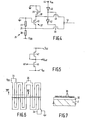
- Fig. 4 shows the circuit diagram of an input circuit according to the invention, which is so constructed as to prevent pn junctions being biased (due to the said cross-talk) in the forward direction and thus leading to signal distortion.
- the circuit comprises for this purpose a voltage divider 26 comprising two resistance elements 27 and 28 between a reference voltage (earth) and a junction point 29 on the one hand and between the junction 29 and a point at the substrate voltage V BB on the other hand.
- the input diode 11 is connected to the conductor 12 and through a switch 30 to the junction 29.
- the element 28, which is connected to VBB is constituted by an element which is arranged outside the substrate 2. Due to the fact that the element 28, which is connected to the lowest potential of all circuit elements of the unput circuit, is arranged outside the substrate 2 (surface region 4) and therefore does not form a pn junction with the substrate, potential fluctuations in the substrate will not or at least substantially not influence the element 28. Due to the fact that furthermore the remaining circuit elements or parts thereof are applied to a higher potential, pn junctions formed by these elements (or parts thereof) with the substrate will always remain cut off even when potential fluctuations occur in the substrate owing to clock cross-talk.
- the voltage divider, or at least the element 28, can be constituted by elements or an element arranged outside the envelope in which the charge-coupled device is usually provided.
- the resistance element 28 is arranged on top of the semiconductor body 2, more particularly as a resistor of polycrystalline silicon material.
- the resistance element 27 may comprise, if desired, a conventional MOS transistor, which is formed in the body 2.
- the element 27 is also constituted by a resistor of polycrystalline silicon.
- Figures 6 and 7 show a plan view and a cross- section, respectively, of the voltage divider 26.
- the resistor is provided on the comparatively thick oxide layer 32, which covers the parts of the surface 4 lying outside the active parts.
- the resistors 27, 28 can be made of the the same polycrystalline silicon layer as the clock electrodes 7a, 8a.
- the sheet resistance of his layer is about 30 ⁇ .
- the resistor is folded, as a result of which a meander-shaped structure is formed having an overall resistance lying between 10 and 15 k ⁇ .
- the meander structure comprises three connections, i.e. the connections 33 and 34 at the ends which are connected to V BB and earth, respectively, and the connection 35 which corresponds to the junction 29 in Fig. 4.
- the area of connection 29 can be accurately determined from the ratio of the resistors 27 and 28.
- the poly material can be coated, after the definition of the meander structure, with thermal oxide 36 whilst simultaneously applying the oxide to the poly electrodes 7a and 8a.
- Contact holes can be provided in this oxide layer at the area of the connection surfaces 33-35, after which in known manner Al contacts and Al conductor tracks can be formed.
- the reference level for the "0" signal is generated by the voltage divider 37, the reference voltage being derived from the junction point 38 between the two resistance elements.
- the voltage divider 37 which is connected between earth and the junction 29 may have a construction similar to that of the voltage divider 26. In the present embodiment, however, the voltage divider 37 comprises a third resistance element 39 and a fourth resistance element 40 in the form of field effect transistors, the transistor 39 being connected between earth and the junction 38 and the transistor 40 being connected between the junction 38 and the junction 29.
- the gate electrodes of the transistors 39 and 40 are connected to earth.
- the potential at point 38 for example -0.2V, can be adjusted in a simple manner by those skilled in the art by means of the geometric ratio of the transistors 39 and 40.
- the junction 38 is connected through a switch comprising a MOS transistor 41 and through the connection (conductor) 12 to the input diode 11.
- the gates of the MOS transistors 30 and 41 are connected to the outputs of two series-connected inverter circuits 42 and 43, respectively.
- the output signal of the inverter circuit 42 is high again so that the transistor 30 is conducting and the input diode 11 is connected through conductors 12 to the point 29 .
- the inverter circuits 42, 43 may have a known construction as shown in Fig. 5.
- the circuit arrangement comprises an inverter transistor 45, whose source zone is connected to V SS (earth).
- the input signals are supplied via the terminal 46 to the gate electrode of the transistor 45.
- the drain of the transistor 45 is connected to the source of a load transistor 47.
- the gate electrode of this transistor - which is of the depletion type - is connected to its source.
- the drain of the transistor 47 is connected to the positive supply source V dd .
- the output signal of the inverter circuit can be derived at the terminal V ou t.
- the lowest potential occurring in the inverter circuits 42, 43 is the earth potential V SS . Since this potential is considerably higher than V BB9 there will be no or substantially no risk also in the inverter circuits 42, 43 that pn junctions in the inverter circuits will be connected in the forward direction due to clock cross-talk between the substrate and the clock electrodes.
- the invention is not limited to the embodiment described, but that many further modifications are possible for those skilled inthe art without departing from the scope of the invention.
- the invention may advantageously be used in other types of charge-coupled devices than described herein, such as, for example, in 1 bit/electrode charge-coupled devices, in which in a group of m successive electrodes (m-1) bits are stored and in which the transport takes place by displacing the empty bucket in the direction opposite to the charge transport direction.
- the resistance element 28 may alternatively be constituted by a circuit element other than a resistor, for example a MOS transistor formed in the polycrystalline silicon layer.
Landscapes
- Solid State Image Pick-Up Elements (AREA)
- Metal-Oxide And Bipolar Metal-Oxide Semiconductor Integrated Circuits (AREA)
- Semiconductor Integrated Circuits (AREA)
Applications Claiming Priority (2)
| Application Number | Priority Date | Filing Date | Title |
|---|---|---|---|
| NL8501542 | 1985-05-30 | ||
| NL8501542A NL8501542A (nl) | 1985-05-30 | 1985-05-30 | Ladingsgekoppelde inrichting. |
Publications (2)
| Publication Number | Publication Date |
|---|---|
| EP0205203A1 true EP0205203A1 (fr) | 1986-12-17 |
| EP0205203B1 EP0205203B1 (fr) | 1990-09-05 |
Family
ID=19846061
Family Applications (1)
| Application Number | Title | Priority Date | Filing Date |
|---|---|---|---|
| EP86200908A Expired - Lifetime EP0205203B1 (fr) | 1985-05-30 | 1986-05-23 | Dispositif à couplage de charges |
Country Status (9)
| Country | Link |
|---|---|
| US (1) | US4727560A (fr) |
| EP (1) | EP0205203B1 (fr) |
| JP (1) | JPS61276370A (fr) |
| KR (1) | KR860009429A (fr) |
| AU (1) | AU5791786A (fr) |
| CA (1) | CA1256996A (fr) |
| DE (1) | DE3673879D1 (fr) |
| IE (1) | IE57419B1 (fr) |
| NL (1) | NL8501542A (fr) |
Families Citing this family (14)
| Publication number | Priority date | Publication date | Assignee | Title |
|---|---|---|---|---|
| US4896340A (en) * | 1985-11-01 | 1990-01-23 | Hughes Aircraft Company | Partial direct injection for signal processing system |
| JPH02276096A (ja) * | 1989-04-17 | 1990-11-09 | Sony Corp | ゲート入力方式の電荷転送装置 |
| US5497140A (en) * | 1992-08-12 | 1996-03-05 | Micron Technology, Inc. | Electrically powered postage stamp or mailing or shipping label operative with radio frequency (RF) communication |
| DE4217408C1 (de) * | 1992-05-26 | 1993-11-25 | Texas Instruments Deutschland | Integrierter Spannungsteiler |
| US6045652A (en) * | 1992-06-17 | 2000-04-04 | Micron Communications, Inc. | Method of manufacturing an enclosed transceiver |
| US5776278A (en) * | 1992-06-17 | 1998-07-07 | Micron Communications, Inc. | Method of manufacturing an enclosed transceiver |
| US5779839A (en) * | 1992-06-17 | 1998-07-14 | Micron Communications, Inc. | Method of manufacturing an enclosed transceiver |
| DE4319878A1 (de) * | 1992-06-17 | 1993-12-23 | Micron Technology Inc | Hochfrequenz-Identifikationseinrichtung (HFID) und Verfahren zu ihrer Herstellung |
| USRE42773E1 (en) | 1992-06-17 | 2011-10-04 | Round Rock Research, Llc | Method of manufacturing an enclosed transceiver |
| US7158031B2 (en) | 1992-08-12 | 2007-01-02 | Micron Technology, Inc. | Thin, flexible, RFID label and system for use |
| US5988510A (en) * | 1997-02-13 | 1999-11-23 | Micron Communications, Inc. | Tamper resistant smart card and method of protecting data in a smart card |
| US6329213B1 (en) | 1997-05-01 | 2001-12-11 | Micron Technology, Inc. | Methods for forming integrated circuits within substrates |
| US6339385B1 (en) * | 1997-08-20 | 2002-01-15 | Micron Technology, Inc. | Electronic communication devices, methods of forming electrical communication devices, and communication methods |
| US6273339B1 (en) | 1999-08-30 | 2001-08-14 | Micron Technology, Inc. | Tamper resistant smart card and method of protecting data in a smart card |
Citations (2)
| Publication number | Priority date | Publication date | Assignee | Title |
|---|---|---|---|---|
| WO1982001962A1 (fr) * | 1980-12-01 | 1982-06-10 | Aircraft Co Hughes | Circuit d'entree a modulation de porte pourvue de resistances de silicium polycristallin |
| EP0133721A1 (fr) * | 1983-08-02 | 1985-03-06 | Koninklijke Philips Electronics N.V. | Dispositif semi-conducteur |
Family Cites Families (1)
| Publication number | Priority date | Publication date | Assignee | Title |
|---|---|---|---|---|
| US4191896A (en) * | 1976-07-26 | 1980-03-04 | Rca Corporation | Low noise CCD input circuit |
-
1985
- 1985-05-30 NL NL8501542A patent/NL8501542A/nl not_active Application Discontinuation
-
1986
- 1986-04-25 US US06/855,652 patent/US4727560A/en not_active Expired - Fee Related
- 1986-05-23 EP EP86200908A patent/EP0205203B1/fr not_active Expired - Lifetime
- 1986-05-23 DE DE8686200908T patent/DE3673879D1/de not_active Expired - Lifetime
- 1986-05-26 AU AU57917/86A patent/AU5791786A/en not_active Abandoned
- 1986-05-27 IE IE1393/86A patent/IE57419B1/en unknown
- 1986-05-28 CA CA000510223A patent/CA1256996A/fr not_active Expired
- 1986-05-28 JP JP61121359A patent/JPS61276370A/ja active Granted
- 1986-05-30 KR KR1019860004278A patent/KR860009429A/ko not_active Withdrawn
Patent Citations (2)
| Publication number | Priority date | Publication date | Assignee | Title |
|---|---|---|---|---|
| WO1982001962A1 (fr) * | 1980-12-01 | 1982-06-10 | Aircraft Co Hughes | Circuit d'entree a modulation de porte pourvue de resistances de silicium polycristallin |
| EP0133721A1 (fr) * | 1983-08-02 | 1985-03-06 | Koninklijke Philips Electronics N.V. | Dispositif semi-conducteur |
Non-Patent Citations (1)
| Title |
|---|
| RCA REVIEW, vol. 36, no. 3, September 1975, pages 566-593, Princeton, US; W.F. KOSONOCKY et al.: "Basic concepts of charge-coupled devices" * |
Also Published As
| Publication number | Publication date |
|---|---|
| IE57419B1 (en) | 1992-08-26 |
| DE3673879D1 (de) | 1990-10-11 |
| EP0205203B1 (fr) | 1990-09-05 |
| US4727560A (en) | 1988-02-23 |
| KR860009429A (ko) | 1986-12-22 |
| JPH0480542B2 (fr) | 1992-12-18 |
| IE861393L (en) | 1986-11-30 |
| CA1256996A (fr) | 1989-07-04 |
| AU5791786A (en) | 1986-12-04 |
| NL8501542A (nl) | 1986-12-16 |
| JPS61276370A (ja) | 1986-12-06 |
Similar Documents
| Publication | Publication Date | Title |
|---|---|---|
| US4044373A (en) | IGFET with gate protection diode and antiparasitic isolation means | |
| US4012759A (en) | Bulk channel charge transfer device | |
| EP0205203B1 (fr) | Dispositif à couplage de charges | |
| US3934159A (en) | Semiconductor circuit devices using insulated gate-type field effect elements having protective diodes | |
| US3913077A (en) | Serial-parallel-serial ccd memory with interlaced storage | |
| US4993053A (en) | Charge transfer device provided with an improved output stage | |
| HK147895A (en) | Integrated circuit with "latch-up" protective circuit in complementary mos circuit techniques | |
| US4110777A (en) | Charge-coupled device | |
| US4725875A (en) | Memory cell with diodes providing radiation hardness | |
| US4584697A (en) | Four-phase charge-coupled device having an oversized electrode | |
| EP0161023B1 (fr) | Dispositif semi-conducteur à couplage de charges avec commande dynamique | |
| US4139782A (en) | Regenerator stage for CCD arrangements | |
| US4207477A (en) | Bulk channel CCD with switchable draining of minority charge carriers | |
| US4272693A (en) | Analysis circuit for a charge coupled device | |
| US4691218A (en) | Charge transfer device | |
| CA1291566C (fr) | Dispositif semiconducteur | |
| US4333022A (en) | Semiconductor device for digitizing an electric analog signal | |
| US3918081A (en) | Integrated semiconductor device employing charge storage and charge transport for memory or delay line | |
| US4178519A (en) | Input circuit for charge transfer apparatus | |
| US3908182A (en) | Non-volatile memory cell | |
| US4449142A (en) | Semiconductor memory device | |
| US4223329A (en) | Bipolar dual-channel charge-coupled device | |
| EP0257347B1 (fr) | Arrangement de semi-conducteur equipé d'un condensateur à tranchée pour empêcher le mauvais fonctionnement d'un circuit | |
| US4359651A (en) | Anti-blooming input structure for charge transfer device | |
| EP0458407A2 (fr) | Echantillonnage d'un signal de tension analogique |
Legal Events
| Date | Code | Title | Description |
|---|---|---|---|
| PUAI | Public reference made under article 153(3) epc to a published international application that has entered the european phase |
Free format text: ORIGINAL CODE: 0009012 |
|
| AK | Designated contracting states |
Kind code of ref document: A1 Designated state(s): DE FR GB IT |
|
| 17P | Request for examination filed |
Effective date: 19870515 |
|
| 17Q | First examination report despatched |
Effective date: 19891009 |
|
| GRAA | (expected) grant |
Free format text: ORIGINAL CODE: 0009210 |
|
| AK | Designated contracting states |
Kind code of ref document: B1 Designated state(s): DE FR GB IT |
|
| REF | Corresponds to: |
Ref document number: 3673879 Country of ref document: DE Date of ref document: 19901011 |
|
| ITF | It: translation for a ep patent filed | ||
| ET | Fr: translation filed | ||
| PG25 | Lapsed in a contracting state [announced via postgrant information from national office to epo] |
Ref country code: GB Effective date: 19910523 |
|
| PLBE | No opposition filed within time limit |
Free format text: ORIGINAL CODE: 0009261 |
|
| STAA | Information on the status of an ep patent application or granted ep patent |
Free format text: STATUS: NO OPPOSITION FILED WITHIN TIME LIMIT |
|
| 26N | No opposition filed | ||
| GBPC | Gb: european patent ceased through non-payment of renewal fee | ||
| PG25 | Lapsed in a contracting state [announced via postgrant information from national office to epo] |
Ref country code: FR Effective date: 19920131 |
|
| PG25 | Lapsed in a contracting state [announced via postgrant information from national office to epo] |
Ref country code: DE Effective date: 19920303 |
|
| REG | Reference to a national code |
Ref country code: FR Ref legal event code: ST |
|
| PG25 | Lapsed in a contracting state [announced via postgrant information from national office to epo] |
Ref country code: IT Free format text: LAPSE BECAUSE OF NON-PAYMENT OF DUE FEES;WARNING: LAPSES OF ITALIAN PATENTS WITH EFFECTIVE DATE BEFORE 2007 MAY HAVE OCCURRED AT ANY TIME BEFORE 2007. THE CORRECT EFFECTIVE DATE MAY BE DIFFERENT FROM THE ONE RECORDED. Effective date: 20050523 |