EP0205923B1 - Circuit de fixation automatique du niveau de suppression - Google Patents
Circuit de fixation automatique du niveau de suppression Download PDFInfo
- Publication number
- EP0205923B1 EP0205923B1 EP86106841A EP86106841A EP0205923B1 EP 0205923 B1 EP0205923 B1 EP 0205923B1 EP 86106841 A EP86106841 A EP 86106841A EP 86106841 A EP86106841 A EP 86106841A EP 0205923 B1 EP0205923 B1 EP 0205923B1
- Authority
- EP
- European Patent Office
- Prior art keywords
- circuit
- pedestal level
- level
- auto
- converter
- Prior art date
- Legal status (The legal status is an assumption and is not a legal conclusion. Google has not performed a legal analysis and makes no representation as to the accuracy of the status listed.)
- Expired
Links
- NJPPVKZQTLUDBO-UHFFFAOYSA-N novaluron Chemical compound C1=C(Cl)C(OC(F)(F)C(OC(F)(F)F)F)=CC=C1NC(=O)NC(=O)C1=C(F)C=CC=C1F NJPPVKZQTLUDBO-UHFFFAOYSA-N 0.000 claims description 75
- 239000003990 capacitor Substances 0.000 claims description 31
- 230000000903 blocking effect Effects 0.000 claims description 14
- 239000002131 composite material Substances 0.000 description 35
- 238000009499 grossing Methods 0.000 description 26
- 238000010586 diagram Methods 0.000 description 16
- 230000003247 decreasing effect Effects 0.000 description 13
- 230000007935 neutral effect Effects 0.000 description 11
- 239000000872 buffer Substances 0.000 description 10
- 238000007599 discharging Methods 0.000 description 4
- 230000001902 propagating effect Effects 0.000 description 4
- 230000004044 response Effects 0.000 description 4
- 230000008859 change Effects 0.000 description 3
- 239000004973 liquid crystal related substance Substances 0.000 description 3
- 230000004048 modification Effects 0.000 description 2
- 238000012986 modification Methods 0.000 description 2
- 238000005070 sampling Methods 0.000 description 2
- 238000006243 chemical reaction Methods 0.000 description 1
- 239000000470 constituent Substances 0.000 description 1
- 230000000694 effects Effects 0.000 description 1
- 230000006872 improvement Effects 0.000 description 1
- 230000002452 interceptive effect Effects 0.000 description 1
- 230000002035 prolonged effect Effects 0.000 description 1
- 230000009467 reduction Effects 0.000 description 1
Images
Classifications
-
- H—ELECTRICITY
- H04—ELECTRIC COMMUNICATION TECHNIQUE
- H04N—PICTORIAL COMMUNICATION, e.g. TELEVISION
- H04N5/00—Details of television systems
- H04N5/14—Picture signal circuitry for video frequency region
- H04N5/16—Circuitry for reinsertion of DC and slowly varying components of signal; Circuitry for preservation of black or white level
- H04N5/18—Circuitry for reinsertion of DC and slowly varying components of signal; Circuitry for preservation of black or white level by means of "clamp" circuit operated by switching circuit
Definitions
- the present invention relates to an improvement in an auto-pedestal level clamp circuit in an automatic luminance control circuit of a television.
- an auto-pedestal level clamp circuit is adapted to forcibly clamp the pedestal level at a given level.
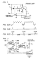
- Fig. 1 shows a conventional auto-pedestal clamp circuit.
- reference numeral 1 denotes a control for generating a divided voltage of a positive power source voltage (to be referred to as V oo hereinafter) and a negative power source voltage (to be referred to as V ss hereinafter); 2, a diode; 4, 5, 9, 10, capacitors; 3, 6, and 8, resistors; 7, a transistor; 11, a pedestal level clamp switch which is turned on or off in response to a pedestal level clamp pulse; and 12, an A/D converter for quantizing the composite video signal.
- V oo positive power source voltage
- V ss negative power source voltage
- the diode 2 connected to an intermediate tap of the control 1 clamps a composite video signal passing through the capacitor 5, and the clamped signal is smoothed by the resistor 3 and the capacitor 4.
- the collector potential of the transistor 7 varies depending on the change in smoothed potential, thus charging or discharging the capacitor 9. More specifically, in a bright frame (i.e., when a luminance signal in the composite video signal is high), since the base potential of the transistor 7 increases, the collector current increases accordingly, and the capacitor 9 discharges, thus decreasing the potential of the capacitor 9. On the other hand, in a dark frame (when the luminance signal is low), the capacitor 9 is charged, and its potential increases.
- Figs. 2(A) to 2(C) are timing charts showing the relationship between the pedestal level clamp pulse and the ON/OFF operation of the pedestal level clamp switch with respect to the composite video signal during about 2H (H: horizontal period) of the composite video signal.
- Fig. 2(A) shows the composite video signal
- Fig. 2(B) shows the pedestal clamp pulse which goes to HIGH level during an interval from the leading edge of a horizontal sync signal to the luminance signal in the composite video signal from which DC components are removed (this interval will be referred to as a back porch hereinafter).
- the auto-pedestal level clamp circuit is necessary for enabling averaged display by narrowing the dynamic range determined by an A/D converter and the like, so that the pedestal level is decreased in a bright frame to display many bright image portions and increased in a dark frame to display many dark image portions.
- the control 1 in Fig. 1 must be finely adjusted, resulting in increased number of steps and hence increased cost.
- the capacitors 4, 5, and 9 have a capacitance of 0.1 to several tens of uF, they cannot be integrated as an IC and must be separately arranged, thus interfering with cost reduction and compact circuit design.
- the output from the A/D converter in Fig. 1 is not fed back for setting the pedestal level, a time constant for circuit constituents must be accurately selected, thus narrowing the application range with respect to the amplitude of the composite video signal.
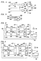
- Fig. 3 is a block diagram of an auto-pedestal level clamp circuit according to an embodiment of the present invention. Arrows in Fig. 3 indicate propagating directions of signals.
- Reference numeral 101 denotes a luminance signal period signal indicating a period in a composite video signal during which a luminance signal is present; 103 and 102, most and least significant comparator outputs from an A/D converter, respectively; 104, a first gate receiving the least significant comparator output 102 from the A/D converter and the luminance period signal 101 to synthesize a first switch control signal; 105, a second gate receiving the most significant comparator output 103 from the A/D converter and the luminance period signal 101 to synthesize a second switch control signal; 106 and 107, outputs from the first and second gates 104 and 105 for controlling the first and second switches, respectively; 108 and 109, first and second switches each having one end connected to V DD and V ss , respectively; 110, a smoothing circuit connected to the node between the first
- the first gate 104 causes the first switch 108 to be closed, thus connecting the smoothing circuit 110 to voltage V DD .
- the second gate 105 causes the second switch 109 to be closed, thus connecting the smoothing circuit 110 to voltage V ss .
- the first and second gates 104 and 105 open the first and second switches 108 and 109 and supply no input to the smoothing circuit 110.
- Fig. 4 is a circuit of the first and second gates 104 and 105, the switches 108 and 109, and the smoothing circuit 110 shown in Fig. 3 and a control circuit for producing a luminance signal period signal 101 shown in Fig. 3 and controlling the operation during the non-display period.
- the same reference numerals in Fig. 4 denote the same parts as in Fig. 3.
- Reference numeral 201 denotes an AND gate for controlling the first and second switches 108 and 109 to be opened during the non-display period; 202, a NAND gate serving as the first gate; 203 and 204, an inverter and a NOR gate, which constitute the second gate; 205, a P-MOSFET used as the first switch; 206, an N-MOSFET used as the second switch; 207 and 208, a resistor and a capacitor, which constitute a smoothing circuit; and 209 and 210, signals which go to LOW level during the vertical and horizontal blanking periods.
- the outputs 102 and 103 from the least and most significant comparators of the A/D converter go to LOW level, and the N-MOSFET 206 is enabled.
- the N-and P-MOSFETs 205 and 206 are disabled.
- Fig. 5 is a circuit diagram of another circuit when quantized outputs from the A/D converter are used as first and second luminance signal level detectors.
- reference numeral 301 denotes a NOR gate; 302, a NAND gate; and 303, 304, 305, and 306, outputs from the 4-bit A/D converter.
- the outputs from the NAND gate 302 and the NOR gate 301 go to LOW level.
- first and second switches can be bipolar transistors, and the present invention can be applied to a CRT display type television. In order to reduce power consumption, the first and second switches can be operated during every few Hs.
- Fig. 6 is a block diagram of an auto-pedestal clamp circuit according to a second embodiment of the present invention. Referring to Fig. 6, arrows indicate propagating directions of signals, and the same reference numerals therein denote the same parts as in Fig. 3.
- Reference numeral 401 denotes a first gate circuit for making a "dark” judgement based on the output from a luminance signal level detector when a luminance signal level is low, to pass continuously input clocks (indicated by 412) therethrough; 402, a first counter circuit for counting the clocks (indicated by 415) passing through the first gate circuit 401 during a specific period for judging total level of the luminance signal; 403, a first latch circuit for latching an "overall bright” or “overall dark” judgement indicated by 418 as the output from the first counter circuit 402 when the specific period is completed; 404, a first switch which is connected to a DC potential V DD and is closed when the output (indicated by 421) from the first latch circuit 403 indicates an "overall dark” judgement; 405, a second gate circuit for making a "bright” judgement based on the output from the luminance signal level detector when the luminance signal level is high, to pass the clocks 412 therethrough; 406, a second counter circuit for counting the clocks
- reference numeral 112 denotes a pedestal level clamp pulse; 424, a signal for fetching the outputs 418 and 419 from the first and second counter circuits 402 and 406 by the first and second latch circuits 403 and 407 when the specific period is completed; and 116, 4-bit quantized outputs from the A/D converter 115.
- the luminance signal includes many underflow portions and indicates an "overall dark” judgement
- the period during which the clocks 412 can pass through the first gate 401 is prolonged.
- the first counter circuit 402 makes an "overall dark” judgement, and the result 418 is fetched by the first latch circuit 403 when the specific period is completed.
- the period during which the clocks 412 can pass through the second gate circuit 405 is shortened, and the outputs 416 from the second gate circuit 405 input to the second counter circuit 406 cannot exceed a count value set, in advance, for making an "overall bright” judgement during the specific period.
- the second counter circuit 406 thus makes an "overall dark” judgement, and the result 419 is fetched by the second latch circuit 407 when the specific period is completed.
- the first switch 404 is closed and the second switch 408 is opened by the outputs 421 and 422 from the first and second latch circuits 403 and 407, and the pedestal level clamp switch 113 is closed.
- charges flow into the DC blocking capacitor 114 due to charging characteristics determined by the resistances of the switches 404 and 113 and the capacitance of the capacitor 114, thereby increasing the pedestal level of the composite video signal supplied to the A/D converter 115.
- the clocks 412 can pass through the first gate circuit 401 for only a short period. However, since they can pass through the second gate circuit 406 for a long period, the clock outputs 415 of the first gate circuit401 are below the preset count value of the first counter circuit 402 for making an "overall dark” judgement during the specific period, and the first counter circuit 402 then makes an "overall bright” judgement. In addition, since the clock outputs 416 exceed the preset count value of the second counter circuit 406 for making an "overall bright” judgement, the second counter circuit 406 makes an "overall bright” judgement. The respective results 418 and 419 are fetched by the first and second latch circuits 403 and 407 when the specific period is completed.
- the first and second switches 404 and 408 are opened during the next specific period, thus disabling pedestal level control.
- both the first and second counter circuits 402 and 406 make an "overall dark" judgement during the preceding specific period, the pedestal level of the composite video signal input to the A/ D converter 115 is slightly increased during the next specific period, and the luminance signal level input thereto is also increased accordingly, thus forming a feedback loop to approach a neutral state.
- the feedback operation can be smoothed.
- the second embodiment is particularly effective with respect to small-amplitude composite video signals.
- the pedestal level clamp switch can be omitted.
- the clocks passing through the first and second gate circuits can be sampling clocks from the A/D converter or inverted clocks therefrom.
- a variable or fixed resistor is connected between the pedestal level clamp switch 113 and the node between the first and second switches 404 and 408, to control the DC potential (e.g., V oo or V ss ).
- the above resistor can be selected so that a change in resistance thereof due to temperature corresponds to an optimal adjustment value.
- the circuit of this embodiment can be applied to a CRT display type television.
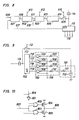
- Fig. 7 is a block diagram of an auto-pedestal clamp circuit according to a third embodiment of the present invention. Referring to Fig. 7, arrows indicate propagating directions of signals, and the same reference numerals therein denote the same parts as in Fig. 6.
- This embodiment is similar to that shown in Fig. 6, except that a comparator 501 for comparing count values from first and second counter circuits 402 and 406 is provided.
- First and second counter circuits 402 and 406 are reset when a specific period begins.
- a luminance signal during the specific period includes many underflow portions, the number of clocks 412 which can pass through a first gate circuit 401 is increased, and the number passing through a second gate circuit 405 is decreased.
- the comparator 501 then compares count outputs 418 and 419 from the first and second counter circuits 402 and 406 when the specific period is completed.
- a first latch circuit 403 fetches the result "too dark”
- a second latch circuit 407 fetches the result "not too bright”.
- the comparator 501 judges within its precision range that the count outputs 418 and 419 from the first and second counter circuits 402 and 406 are the same when the specific period is completed, and the first and second latch circuits 403 and 407 respectively fetch the results "not too dark” and “not too bright” from the comparator 501.
- both the first and second switches 404 and 408 are opened, and the pedestal level of the composite video signal input to the A/D converter 115 remains unchanged.
- the pedestal level clamp switch can be omitted.
- the clocks passing through the first and second gate circuits can be sampling clocks from the A/D converter or inverted clocks therefrom.
- a variable or fixed resistor is connected between the pedestal level clamp switch 113 and the node between the first and second switches 404 and 408 to control the DC potential (e.g., V ⁇ or V ss ).
- the above resistor can be selected so that a change in resistance thereof due to temperature corresponds to an optimal adjustment value.
- the circuit of this embodiment can be applied to a CRT display type television.
- Fig. 8 is a block diagram of an auto-pedestal level clamp circuit according to a fourth embodiment of the present invention.
- reference numeral 601 denotes a gate circuit which passes continuously input clocks (indicated by 608) therethrough when a luminance signal level is high;
- 602 a counter circuit which is initialized by a reset signal (indicated by 610) when a specific period for judging the total level of the luminance signal begins, and counts the clock outputs passing through the gate circuit 601 (indicated by 609) during the specific period;
- 603 a latch circuit for latching an "overall bright", “overall dark”, or "neutral brightness” judgement as 2-bit output from the counter circuit 602 (indicated by 611) in response to a fetching clock (indicated by 618) when the specific period is completed;
- 604 an adjusting circuit for generating a DC potential based on the 2-bit output from the latch circuit 603 (indicated by 613);
- 605 an adjusting circuit for generating
- the number of the clocks 608 passing through the gate circuit 601 is increased, and the outputs 609 input therefrom to the counter circuit 602 exceed two count values set for making an "overall dark” and “not overall dark” judgement during the specific period.
- the counter circuit 602 then makes an "overall bright” judgement, and the output result 611 is fetched by the latch circuit 603 when the specific period is completed.
- the counter circuit 102 makes an "overall dark” judgement, and the output result 611 is latched by the latch circuit 603 when the specific period is completed.
- the averaged luminance signal level is a neutral value and indicates "neutral brightness”
- the number of clock outputs 609 having passed through the gate circuit 601 exceeds the count value for making a "not overall dark” judgement but is below the count value for an "overall bright” judgement during the specific period.
- the counter circuit 602 makes a "neutral brightness” judgement, and the output result 111 is latched by the latch circuit 603 when the specific period is completed.
- the latch circuit 603 latches the output 611 indicating an "overall dark” judgement from the counter circuit 602 since the adjusting circuit 604 generates the high potential V DD as its output 614, the pedestal level is increased.
- the latch circuit 603 latches the output 611 indicating "neutral brightness” from the counter circuit 602
- the output 614 from the adjusting circuit 604 has high impedance, and charge flow through the pedestal level clamp switch 605 is interrupted, thus keeping the pedestal level unchanged.
- the pedestal level of the composite video signal input to the A/D converter 115 is slightly increased in the next period, and the luminance signal level input thereto is decreased accordingly, thus forming a feedback loop for approaching a "neutral brightness” state.
- the pedestal level is controlled to approach the neutral state.
- the auto-pedestal level clamp circuit can be arranged using only "overall bright” and “overall dark” judgements without "neutral brightness” in the embodiment shown in Fig. 8.
- the 2-bit output 613 from the latch circuit 603 in Fig. 8 can be reduced to 1 bit, and the latch circuit 603 can be simplified. This enhances the feedback effect of the auto-pedestal level clamp operation.
- the clocks can easily pass through the gate circuit 601 when the luminance signal level is high, but the circuit can also be constituted such that the clocks pass therethrough when the luminance signal level is low.
- Fig. 9 is a block diagram of an auto-pedestal level clamp circuit according to a fifth embodiment of the present invention.
- reference numeral 114 denotes a DC blocking capacitor for an input composite video signal; 702, a 4-bit A/D converter for A/D converting the composite video signal which has passed through the capacitor 114 and is pedestal- clamped; 703, 704, 705, and 706, 3-state buffers which perform an inverter operation during a luminance signal period of the composite video signal; 707, 708, 709, and 710, resistors having resistances determined in accordance with weighting according to the output from the A/D converter 702; 711, a resistor for a smoothing circuit; 712, a capacitor for the smoothing circuit; 113, a pedestal level clamp switch; 112, a pedestal level clamp pulse for opening/closing the pedestal level clamp switch 113; 715, a signal for controlling the inverter operation output from the 3-state buffers 703, 704, 705, and 706 and high-i
- the resistance of the resistor 707, connected to the output of the 3-state buffer 703 to which the 2 3- bit output 716 from the A/D converter 702 is input is RQ
- the resistances of the resistors 708, 709, and 710, respectively connected to the outputs of the 3-state buffers 704, 705, and 706 to which the 22-, 2'-, and 2°-bit outputs 717, 718, and 719 are input are weighted to be 2RQ, 4RQ, and 8R ⁇ , respectively, thus constituting an adder circuit. Therefore, the signal input to the smoothing circuit 721 corresponds to an inverted, D/A converted signal of the composite video signal input to the A/D converter 702 during the inverter operation of the 3-state buffers 703, 704, 705, and 706.
- the input signal of the smoothing circuit 721 which is substantially the same as an inverted luminance signal, includes many low potential portions, and the output voltage from the smoothing circuit 721 is decreased.
- the pedestal level clamp switch 113 is closed, charges flow from the DC blocking capacitor 114 into the smoothing circuit 721, and the pedestal level of the composite video signal input to the A/D converter 702 is decreased.
- the input signal of the smoothing circuit 721, which is substantially the same as the luminance signal input to the A/D converter 702 includes many high potential portions.
- the output from the smoothing circuit 721 is increased, as is the pedestal level.
- the output from the A/D converter 702 causes the input signal to be negatively fed back through the inversion weighting circuit 720, the smoothing circuit 721, and the pedestal level clamp switch 113. Then, the pedestal level can be stabilized to darken the bright frame or to brighten the dark frame.
- Fig. 10 is a circuit diagram of the 3-state buffer used in the inversion weighting circuit of the above embodiment.
- reference numeral 801 denotes an inverter; 802, an OR gate; 803, an AND gate; 804, a P-MOSFET; and 805, an N-MOSFET.
- reference numeral 806 denotes a signal which goes to HIGH level when the 3-state buffer performs the inverter operation during, e.g., the luminance signal period, and goes to LOW level when the 3-state buffer produces the high-impedance output in the horizontal or vertical blanking period; 807, an input terminal receiving the digital outputs 716, 717, 718, and 719 from the A/D converter 702 in Fig.
- a period during which the 3-state buffer produces the high-impedance output corresponds to vertical and horizontal blanking periods of the composite video signal. Since pedestal level control is not influenced by a sync signal and the like except for the luminance signal, a good frame can be obtained.
Landscapes
- Engineering & Computer Science (AREA)
- Multimedia (AREA)
- Signal Processing (AREA)
- Picture Signal Circuits (AREA)
- Transforming Electric Information Into Light Information (AREA)
Claims (10)
Applications Claiming Priority (8)
| Application Number | Priority Date | Filing Date | Title |
|---|---|---|---|
| JP10852485A JPS61265975A (ja) | 1985-05-21 | 1985-05-21 | オ−トペデスタルレベルクランプ回路 |
| JP108524/85 | 1985-05-21 | ||
| JP12677185A JPS61284179A (ja) | 1985-06-11 | 1985-06-11 | オ−トペデスタルレベルクランプ回路 |
| JP126771/85 | 1985-06-11 | ||
| JP60159532A JPH0646787B2 (ja) | 1985-07-19 | 1985-07-19 | オ−トペデスタルレベルクランプ回路 |
| JP159532/85 | 1985-07-19 | ||
| JP191754/85 | 1985-08-30 | ||
| JP60191754A JPH0646788B2 (ja) | 1985-08-30 | 1985-08-30 | オ−トペデスタルレベルクランプ回路 |
Publications (2)
| Publication Number | Publication Date |
|---|---|
| EP0205923A1 EP0205923A1 (fr) | 1986-12-30 |
| EP0205923B1 true EP0205923B1 (fr) | 1990-08-08 |
Family
ID=27469636
Family Applications (1)
| Application Number | Title | Priority Date | Filing Date |
|---|---|---|---|
| EP86106841A Expired EP0205923B1 (fr) | 1985-05-21 | 1986-05-20 | Circuit de fixation automatique du niveau de suppression |
Country Status (4)
| Country | Link |
|---|---|
| US (1) | US4729026A (fr) |
| EP (1) | EP0205923B1 (fr) |
| DE (1) | DE3673255D1 (fr) |
| GB (1) | GB2176670B (fr) |
Families Citing this family (12)
| Publication number | Priority date | Publication date | Assignee | Title |
|---|---|---|---|---|
| JPS6387081A (ja) * | 1986-09-30 | 1988-04-18 | Toshiba Corp | モニタテレビジヨン装置 |
| US4859871A (en) * | 1987-02-13 | 1989-08-22 | Fujitsu Limited | Voltage level setting circuit |
| US5003564A (en) * | 1989-04-04 | 1991-03-26 | Rca Licensing Corporation | Digital signal clamp circuitry |
| US4965669A (en) * | 1989-04-12 | 1990-10-23 | Rca Licensing Corporation | Apparatus for digitally controlling the D.C. value of a processed signal |
| JP2517005Y2 (ja) * | 1989-07-21 | 1996-11-13 | パイオニア株式会社 | 映像信号伸張回路 |
| US5128764A (en) * | 1989-10-27 | 1992-07-07 | Siemens Aktiengesellschaft | Level correcting circuit having switched stages of differing time constants |
| US5027017A (en) * | 1990-01-19 | 1991-06-25 | Rca Licensing Corporation | Sync tip clamp circuitry |
| JP3257788B2 (ja) * | 1990-05-01 | 2002-02-18 | ソニー株式会社 | 画像表示装置 |
| EP0455220B1 (fr) * | 1990-05-02 | 1999-11-03 | Canon Kabushiki Kaisha | Appareil de détection d'image |
| US5448308A (en) * | 1993-02-05 | 1995-09-05 | Thomson Consumer Electronics, Inc. | Apparatus for clamping a video signal level |
| US5610840A (en) * | 1993-09-02 | 1997-03-11 | Asahi Kogaku Kogyo Kabushiki Kaisha | Signal processing device |
| KR100688977B1 (ko) * | 2004-09-13 | 2007-03-08 | 삼성전자주식회사 | 디스플레이 장치 |
Family Cites Families (7)
| Publication number | Priority date | Publication date | Assignee | Title |
|---|---|---|---|---|
| JPS5841709B2 (ja) * | 1973-06-14 | 1983-09-13 | アムペックス コ−ポレ−ション | コウソクドウサノ チヨクリユウクランプカイロソウチ |
| US3970777A (en) * | 1975-06-09 | 1976-07-20 | Minnesota Mining And Manufacturing Company | Apparatus for adjusting video pedestal and peak white level |
| US4013833A (en) * | 1975-08-14 | 1977-03-22 | Samuel Morton Zimmerman | Video system and method for presentation and reproduction of x-ray film images |
| US4403254A (en) * | 1979-08-17 | 1983-09-06 | Sony Corporation | Video signal processing circuit |
| JPS5675780A (en) * | 1979-11-26 | 1981-06-23 | Sony Corp | Video signal processing circuit |
| DE3214756C2 (de) * | 1981-05-02 | 1991-10-17 | Philips Patentverwaltung Gmbh, 2000 Hamburg | Schaltungsanordnung zum Ermitteln des Wertes eines Referenzpegels |
| GB2105547A (en) * | 1981-09-11 | 1983-03-23 | Philips Electronic Associated | Clamping video signals |
-
1986
- 1986-05-20 US US06/865,142 patent/US4729026A/en not_active Expired - Lifetime
- 1986-05-20 DE DE8686106841T patent/DE3673255D1/de not_active Expired - Fee Related
- 1986-05-20 GB GB08612181A patent/GB2176670B/en not_active Expired
- 1986-05-20 EP EP86106841A patent/EP0205923B1/fr not_active Expired
Also Published As
| Publication number | Publication date |
|---|---|
| US4729026A (en) | 1988-03-01 |
| GB2176670A (en) | 1986-12-31 |
| EP0205923A1 (fr) | 1986-12-30 |
| GB8612181D0 (en) | 1986-06-25 |
| GB2176670B (en) | 1988-07-13 |
| DE3673255D1 (de) | 1990-09-13 |
Similar Documents
| Publication | Publication Date | Title |
|---|---|---|
| EP0205923B1 (fr) | Circuit de fixation automatique du niveau de suppression | |
| US6798274B2 (en) | Booster and imaging device using booster | |
| US4859871A (en) | Voltage level setting circuit | |
| JPH0583594A (ja) | アナログ−デジタル変換装置 | |
| US5638123A (en) | Exposure control circuit apparatus | |
| JPH1093436A (ja) | デジタル・アナログ変換回路 | |
| US5345117A (en) | Synchronous separating circuit | |
| US5489946A (en) | High speed sync separation system and method | |
| JPS6220476A (ja) | オ−トペデスタルレベルクランプ回路 | |
| JP2569301B2 (ja) | A/d変換装置 | |
| JPH09261035A (ja) | Cmos装置 | |
| US5872603A (en) | Analog circuit controller using signals indicative of control voltage and type of control voltage | |
| JPS61242473A (ja) | オ−トペデスタルレベルクランプ回路 | |
| JPS6251876A (ja) | オ−トペデスタルレベルクランプ回路 | |
| JPS61265975A (ja) | オ−トペデスタルレベルクランプ回路 | |
| JPS61284179A (ja) | オ−トペデスタルレベルクランプ回路 | |
| JP2596369B2 (ja) | A/d変換装置 | |
| KR950006043B1 (ko) | 칼라 액정소자 뷰파인더의 백 라이트의 자동 밝기 조절회로 | |
| US5889421A (en) | Device for detecting the locking of an automatic gain control circuit | |
| JPH0681285B2 (ja) | A/d変換装置 | |
| JP3231518B2 (ja) | 自動ゲイン調整装置 | |
| KR0113914Y1 (ko) | 캠코더의 영상효과 처리장치 | |
| KR0160118B1 (ko) | 자동이득조절회로 | |
| JP2003023549A (ja) | 信号直流電圧安定化回路およびそれを用いた映像機器 | |
| JPH0670199A (ja) | Ad変換器 |
Legal Events
| Date | Code | Title | Description |
|---|---|---|---|
| PUAI | Public reference made under article 153(3) epc to a published international application that has entered the european phase |
Free format text: ORIGINAL CODE: 0009012 |
|
| AK | Designated contracting states |
Kind code of ref document: A1 Designated state(s): AT BE CH DE FR GB IT LI LU NL SE |
|
| RBV | Designated contracting states (corrected) |
Designated state(s): DE FR GB NL |
|
| 17P | Request for examination filed |
Effective date: 19870217 |
|
| 17Q | First examination report despatched |
Effective date: 19890502 |
|
| GRAA | (expected) grant |
Free format text: ORIGINAL CODE: 0009210 |
|
| AK | Designated contracting states |
Kind code of ref document: B1 Designated state(s): DE FR GB NL |
|
| REF | Corresponds to: |
Ref document number: 3673255 Country of ref document: DE Date of ref document: 19900913 |
|
| ET | Fr: translation filed | ||
| PG25 | Lapsed in a contracting state [announced via postgrant information from national office to epo] |
Ref country code: GB Effective date: 19910520 |
|
| PLBE | No opposition filed within time limit |
Free format text: ORIGINAL CODE: 0009261 |
|
| STAA | Information on the status of an ep patent application or granted ep patent |
Free format text: STATUS: NO OPPOSITION FILED WITHIN TIME LIMIT |
|
| 26N | No opposition filed | ||
| GBPC | Gb: european patent ceased through non-payment of renewal fee | ||
| PGFP | Annual fee paid to national office [announced via postgrant information from national office to epo] |
Ref country code: FR Payment date: 19980511 Year of fee payment: 13 |
|
| PGFP | Annual fee paid to national office [announced via postgrant information from national office to epo] |
Ref country code: DE Payment date: 19980529 Year of fee payment: 13 |
|
| PGFP | Annual fee paid to national office [announced via postgrant information from national office to epo] |
Ref country code: NL Payment date: 19980531 Year of fee payment: 13 |
|
| PG25 | Lapsed in a contracting state [announced via postgrant information from national office to epo] |
Ref country code: NL Free format text: LAPSE BECAUSE OF NON-PAYMENT OF DUE FEES Effective date: 19991201 |
|
| PG25 | Lapsed in a contracting state [announced via postgrant information from national office to epo] |
Ref country code: FR Free format text: LAPSE BECAUSE OF NON-PAYMENT OF DUE FEES Effective date: 20000131 |
|
| NLV4 | Nl: lapsed or anulled due to non-payment of the annual fee |
Effective date: 19991201 |
|
| PG25 | Lapsed in a contracting state [announced via postgrant information from national office to epo] |
Ref country code: DE Free format text: LAPSE BECAUSE OF NON-PAYMENT OF DUE FEES Effective date: 20000301 |
|
| REG | Reference to a national code |
Ref country code: FR Ref legal event code: ST |