EP0206205B1 - Festwertspeicheranordnung - Google Patents
Festwertspeicheranordnung Download PDFInfo
- Publication number
- EP0206205B1 EP0206205B1 EP86108200A EP86108200A EP0206205B1 EP 0206205 B1 EP0206205 B1 EP 0206205B1 EP 86108200 A EP86108200 A EP 86108200A EP 86108200 A EP86108200 A EP 86108200A EP 0206205 B1 EP0206205 B1 EP 0206205B1
- Authority
- EP
- European Patent Office
- Prior art keywords
- transistor
- transistors
- nqmn
- memory device
- read
- Prior art date
- Legal status (The legal status is an assumption and is not a legal conclusion. Google has not performed a legal analysis and makes no representation as to the accuracy of the status listed.)
- Expired
Links
- 239000004065 semiconductor Substances 0.000 claims description 28
- 239000011159 matrix material Substances 0.000 claims description 12
- 230000000295 complement effect Effects 0.000 claims description 11
- 238000010586 diagram Methods 0.000 description 15
- 230000005540 biological transmission Effects 0.000 description 6
- 238000009792 diffusion process Methods 0.000 description 6
- 239000012535 impurity Substances 0.000 description 6
- 238000012986 modification Methods 0.000 description 4
- 230000004048 modification Effects 0.000 description 4
- 238000004519 manufacturing process Methods 0.000 description 3
- 230000006870 function Effects 0.000 description 2
- 230000000630 rising effect Effects 0.000 description 2
- 230000001360 synchronised effect Effects 0.000 description 2
- 230000002457 bidirectional effect Effects 0.000 description 1
- 230000015572 biosynthetic process Effects 0.000 description 1
- 230000000694 effects Effects 0.000 description 1
- 238000000926 separation method Methods 0.000 description 1
- 230000003068 static effect Effects 0.000 description 1
- 230000001052 transient effect Effects 0.000 description 1
Images



Classifications
-
- G—PHYSICS
- G11—INFORMATION STORAGE
- G11C—STATIC STORES
- G11C17/00—Read-only memories programmable only once; Semi-permanent stores, e.g. manually-replaceable information cards
- G11C17/14—Read-only memories programmable only once; Semi-permanent stores, e.g. manually-replaceable information cards in which contents are determined by selectively establishing, breaking or modifying connecting links by permanently altering the state of coupling elements, e.g. PROM
- G11C17/16—Read-only memories programmable only once; Semi-permanent stores, e.g. manually-replaceable information cards in which contents are determined by selectively establishing, breaking or modifying connecting links by permanently altering the state of coupling elements, e.g. PROM using electrically-fusible links
Definitions
- the present invention relates to a read only semiconductor memory device, and more particularly to a read only memory device used in a memory device constituting a CMOS gate array fabricated using the master slice approach.
- gate array LSis are used as circuitry having an intermediate character between microcomputers which obtain various functions utilizing software and custom made LSls based on hard specification of users.
- Such gate array LSIs can obtain desired hardware functions by interconnecting several hundred to thousand of gate circuit blocks provided on a chip in advance on the basis of the users' specification, and they are ordinarily fabricated in accordance with the master slice approach to vary the wiring pattern between unit cells in the wiring area according to the kind of the products so as to meet users' design specification.
- Fig. 1 is a circuit diagram illustrating one example of an essential part of a ROM of the OR type used in a conventional read only semiconductor memory device.
- source grounded n-channel transistors Q11, Q12, Q13, Q21,...., Q23, and Q31 to 033 are arranged in a matrix manner.
- This ROM circuit is provided with word lines WL1, WL2, and WL3 commonly connected to gates of transistors of the same columns, respectively, and bit lines BL1, BL2 and BL3 commonly connected to drains of transistors of the same rows, respectively.
- drains precharging p-channel transistors 01, Q2 and Q3 are connected, respectively wherein their gates are commonly connected to a precharge circuit 1 and their sources are connected to a drain supply voltage V DD (which will be simply called “V DD " hereinafter).
- V DD drain supply voltage
- Their drains of these transistors Q11, Q22 and Q33 are 10 separated from the bit lines BL1, BL2 and BL3, respectively.
- this circuit first is to activate the precharge circuit 1 by a clock signal to place each bit line in high (H) level.
- a transistor connected to the bit line is turned on, with the result that the concerned bit line is pulled down to low (L) level.
- L low
- this circuit can be said as the circuit of synchronous type, giving rise to the problem in use that it is required to precisely adjust the clock for precharge and the timing of an input address signal for selection of the word line.
- Fig. 2 is a circuit diagram illustrating a conventional ROM circuit of the ratio type configured so that bit lines are always respectively pulled up by resistors R1, R2 and R3 instead of the precharge circuit and the p-channel transistors shown in Fig. 1.
- This circuit is of the asynchronous type because the bit lines are always pulled up independent of the selection of the word lines, resulting in no problem in the timing.
- this circuit has the shortcoming that a large d.c. current flows every time the address changes, resulting in large power dissipation.
- Fig. 3 is a circuit diagram illustrating a further conventional ROM circuit used in the gate array in the prior art.
- This circuit is characterized in that the transistors Q11, Q22 and Q33 for producing a predetermined output are arranged so that their sources are connected to V DD instead of separation between the drains and the bit lines as in the prior art, thus providing a ROM of the asynchronous type and having a low power dissipation.
- the circuit threshold voltage V TH of the inverter becomes high. Accordingly, in the event that the H level on the bit line pulled up by the n-channel transistor of which source is connected to V DD by the selection of the word line is lowered by the circuit V TH of the inverter, there is a possibility that this circuit does not normally operate. Namely, the drawback with this circuit is that the range of the threshold voltage V TH is limited, resulting in small margin in the production and poor mass-productivity.
- the memory elements are constituted using only n-channel transistors in the above-mentioned three ROM circuits, the drawback with these circuits is that the p-channel transistor is not used in the CMOS gate array, resulting in low element utilization factor.
- US-A-3 55 00 89 describes a complementary semiconductor matrix array in which pairs of complementary transistors form memory cells.
- the cell transistors are controlled by transistors of the same conductivity type whose gates are connected to complementary word lines and whose drains are connected to row lines.
- the row lines of the matrix connect the sources of the memory cell transistors together and the column lines connect the drains of the memory cell transistors together.
- the word lines are not connected directly to the gates of the memory cell transistors.
- An object of the present invention is to provide a semiconductor ROM device of the asynchronous type having low power dissipation.
- Another object of the present invention is to provide a semiconductor ROM device having excellent mass-productivity.
- a further object of the present invention is to provide a semiconductor ROM device having high element utilization factor.
- a still further object of the present invention is to provide a semiconductor ROM device which securely operates at a high speed.
- a read only semiconductor memory device comprising: a plurality of transistor pairs arranged in a matrix manner, each transistor pair being comprised of a first transistor of one conductivity type and a second transistor of opposite conductivity type and said transistor pairs being arranged such that all first transistors are arranged in first columns and all second transistors are arranged in second columns, input lines for providing one logic state to the gates of the transistors of the first columns, complementary input lines for providing the opposite logic state to the gates of the transistors of the second columns, and output lines for connecting drains of said transistor pairs of the same rows, either one of said first and second transistors being connected to a predetermined logic state to output said predetermined logic state when this transistor is active.
- a read only semiconductor memory device comprising: a plurality of transistor pairs arranged in a matrix manner, each transistor pair being comprised of a first transistor of one conductivity type and a second transistor of opposite conductivity type and said transistor pairs being arranged such that all first transistors are arranged in first columns and all second transistors are arranged in second columns, input lines for providing the one logic state to the gates of the transistors of the first columns, complementary input lines for providing the opposite logic state to the gates of the transistors of the second columns, and output lines for connecting drains of said transistor pairs of the same rows, wherein the transistors of a transistor pair for outputting high level logic state have common source connections and common drain connections, said common source connections being connected to one level voltage supply, and said common drain connections being connected to another level voltage supply, respectively, on said output lines, and wherein the transistors of a transistor pair for outputting low level logic state have connections such that the transistor of said opposite conductivity type pulls down the potential on said output line, when this transistor is active.
- a read only semiconductor memory device of the asynchronous type having low power dissipation and excellent area occupation ratio.
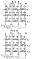
- Fig. 5 is a circuit diagram illustrating an embodiment of a read only semiconductor device according to the present invention.
- a gate array of the master slice type n-channel transistor columns and p-channel transistor columns are arranged alternately on a master chip, ROMs of the OR type are formed.
- each transistor pair comprises n-channel and p-channel transistors commonly connected at their drains. A point at which the drains are commonly connected is connected to a bit line BL.
- Each gate of the n-channel transistors of the same column (first column) is connected to a word line of logic W1 and each gate of the p-channel transistors thereof is connected to a word line of the negative logic W1.
- This negative logic W1 is obtained by branching the word line WL of the logic W1 through an inverter.
- the source of an n-channel transistor NQ11 is in an open state and the source of a p-channel transistor P011 is connected to V DD .
- sources of n-channel transistors NQ21 and NQ31 are connected to a source power supply voltage V ss (which will be simply called “V ss " hereinafter), and sources of p-channel transistors PQ21 and PQ31 are in an open state.
- V ss source power supply voltage
- Fig. 6 is a circuit diagram illustrating a modification of the circuit shown in Fig. 5 wherein transistors of which sources have been placed in an open state, e.g., NQ11. PQ21 and P031, etc. are open also at their gates, respectively.
- This modification has a circuit arrangement such that the word lines are connected only to gates of transistors contributing to the formation of output data. Accordingly, this lessens the load on word lines, thus making it possible to accelerate the word line selective operation.
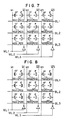
- Fig. 7 is a circuit diagram illustrating another embodiment of a ROM device according to the present invention. This circuit is configured so that the sources of the n-channel transistor and the p-channel transistor of each transistor pair are connected to V ss and V DD , respectively, and the drain of a transistor paired with each transistor producing a specified output is in an open state.
- the drain of the n-channel transistor NQ11 paired with the p-channel transistor PQ11 of the transistor pair giving the meaning of logical "1 and the drains of the p-channel transistors PQ21 and PQ31 paired with the respective n-channel transistors N021 and NQ31 are in an open state.
- drain capacity in the connection between the bit line and the transistor Since this drain capacity affects readout speed, it is preferable that the drain is in an open state.
- the gate of each transistor of which drain is in an open state may be opened, thus reducing the load on word lines.
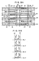
- Fig. 9A is an enlarged plan view illustrating a matrix arrangement shown in Fig. 9B which shows a portion of a ROM circuit having the same configuration as that shown in Fig. 8 realized on a master chip.
- N-channel transistors N011 and NQ12 are comprised of opposing gate electrodes 11 and 12 and n-type impurity diffusion regions 13 intersecting therewith.
- N-channel transistors NQ13 and NQ14 are comprised of opposing gate electrodes 14 and 15 and n-type impurity diffusion regions 16 intersecting therewith.
- P-channel transistors PQ11 and PQ12 are comprised of opposing gate electrodes 17 and 18 and p-type impurity diffusion regions 19.
- p-channel transistors PQ13 and PQ14 are comprised of opposing gate electrodes 20 and 21 and p-type impurity diffusion regions 22 intersecting therewith.
- a V ss line 23 and a W1 word line 24 are formed on the n-channel transistor column.
- a V DD line 26 and a Wf word line 25 are formed on the p-channel transistor column.
- bit lines 27 (BL1), 28 (BL2), 29 (BL3) and 30 (BL4) are arranged in a lateral direction so that they pass on source regions of the n-channel and p-channel transistors. These wirings and each region are connected through contact holes, whereas no contact hole is provided in each opened portion.
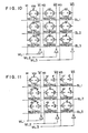
- Fig. 10 is a circuit diagram illustrating a ROM device.
- respective sources and drains are commonly connected to constitute a transmission gate.
- a point at which drains of each transistor pair are commonly connected is connected to each bit line.
- V DD a point at which their sources are commonly connected
- V ss the source common junction
- the source common junction is connected to V DD in the transistor pair NQ11 and PQ11 giving the meaning of logical "1”
- the source common junctions are connected to V ss in the transistor pairs NQ21 and PQ21, and NQ31 and PQ31 giving the meaning of logical "0”.
- Such a transmission gate can perfectly perform level transmission, with the result that it is effective when raising the bit line to H level and is advantageous in the realization of bidirectional transmission.
- Fig. 11 shows an embodiment t of the present invention configured as a modification of Fig. 10.
- the transmission gate is used in each transistor pair used for raising a potential on the bit line, but only the n-channel transistor is used as each transistor used for pulling down a potential on the bit line.
- sources of the n-channel transistors NQ21 and NQ31 are connected to V ss , but drains of the p-channel transistors PQ21 and PQ31 are in an open state, with the result that they do not contribute to pull-down of the potential.
- Fig. 12A is an enlarged plan view illustrating a matrix arrangement shown in Fig. 12B which shows a portion of the circuit shown in Fig. 10 realized on an actual master chip.
- Fig. 12B which shows a portion of the circuit shown in Fig. 10 realized on an actual master chip.
- four n-channel transistors formed by the gates 11, 12, 14 and 15 and n-type impurity diffusion regions 13 and 16 positioned at the left- half and four p-channel transistors formed by gates 17, 18, 20 and 21 and p-type impurity diffusion regions 19 and 22 positioned at the right-half are the same as those in Fig. 9.
- a word line (W1) 31, a V ss line 32, a word line (W2) 33, a word line ( WT ) 34, a V DD line 35 and a word line (W2) 36 are arranged as diffferent layers in a vertical direction, respectively.
- bit lines 37 (BL1) and 38 (BL2) are formed thereon as different layers in a lateral direction, respectively.
- ROMs for realizing logic for gate array have been described in the above-mentioned embodiments, the present invention can be applied to ROMs as memory devices assembled into the gate array or ordinary ROMs.
- the ROM device is configured so that a plurality of transistor pairs each comprising a transistor of one conductivity type and a transistor of an opposite conductivity type are formed in a matrix manner, and that the transistors of the one conductivity type output one memory logic and the transistors of the other conductivity type output the other memory logic. Accordingly, the ROM device effects static operation, thus eliminating the need of the precharge and the clock operations.
- This ROM is essentially configured as a CMOS circuit, resulting in low power consumption. Further, there are used transistors having respective characteristics suitable for raising and pulling down a potential on the output line, leading to large operation margin. Accordingly, this results in a large production margin an improved yield. Furthermore, since p-channel and n-channel transistors which are the same in number are used, element utilization factor is high and a ROM having large capacity and small occupation area can be configured, thus providing an inexpensive and high performance read only semiconductor device.
Landscapes
- Read Only Memory (AREA)
- Semiconductor Memories (AREA)
- Design And Manufacture Of Integrated Circuits (AREA)
Claims (15)
dadurch gekennzeichnet, daß der eine logische Zustand Hochpegel-Logik darstellt und der andere logische Zustand Niedrigpegel-Logik darstellt, wobei der erste Transistor (PQmn) des einen Leitfähigkeitstyps betrieben wird, ein Potential auf der Ausgangsleitung auf hohen Pegel anzuheben, und der zweite Transistor (NQmn) des anderen Leitfähigkeitstyps betrieben wird, ein Potential auf der Ausgangsleitung (BL1, BL2, ...) auf einen niedrigen Pegel herunterzuziehen.
dadurch gekennzeichnet, daß der erste Transistor (POmn) des einen Leitfähigkeitstyps ein p-Kanal-Transistor und der zweite Transistor (NQmn) des entgegengesetzten Leitfähigkeitstyps ein n-KanalTransistor ist.
dadurch gekennzeichnet, daß die Speichervorrichtung als ein CMOS-Haupt-Halbleiterplättchen konfiguriert ist, auf welchem die p-Kanalund n-Kanal-Transistoren (PQmn, NQmn) regelmäßig angeordnet sind.
dadurch gekennzeichnet, daß jede der Eingangsleitungen (WL1, WL2, ...) eine Wortleitung ist, und jede der Ausgangsleitungen (BL1, BL2, ...) eine Bitleitung ist.
dadurch gekennzeichnet, daß ein Transistorpaar (NQmn, PQmn) zum Ausgeben von Hochpegel-Logik einen p-Kanal-Transistor (PQmn) aufweist, dessen Source an eine Drain-Versorgungsspannung (Vdd) angeschlossen ist, dessen Gate mit der Wortleitung (WL1, WL2, ...) verbunden ist, und dessen Drain mit der Bitleitung (BL1, BL2, ...) verbunden ist, und ein Transistorpaar (NQmn, PQmn) zum Ausgeben von Niedrigpegel-Logik einen n-Kanal- Transistor (NQmn) aufweist, dessen Source an eine Source-Versorgungsspannung (Vss) angeschlossen ist, dessen Gate mit einer Wortleitung (WL1, WL2, ...) mit einer zu der Wortleitung entgegengesetzten Logik verbunden ist, und dessen Drain mit der Bitleitung (BL1, BL2, ...) verbunden ist.
dadurch gekennzeichnet, daß ein p-Kanal- Transistor (PQmn) und ein n-Kanal-Transistor (NQmn) eines Transistorpaares einen gemeinsamen Drainanschluß an die Bitleitung (BL1, BL2, ...) haben.
dadurch gekennzeichnet, daß der Transistor der Transistorpaare (NQmn, POmn), welcher keine logische Ausgabe erzeugt, so angeschlossen ist, daß wenigstens Source oder Drain nicht angeschlossen ist.
dadurch gekennzeichnet, daß das Gate des Transistors (NQmn, PQmn), der eine logische Ausgabe nicht erzeugt, nicht mit der Wortleitung (WL1, WL2, ...) verbunden ist.
dadurch gekennzeichnet, daß jedes der Transistorpaare (NQmn, POmn) eine logische Ausgabe einer Einheit einer Gatteranordnung darstellt.
dadurch gekennzeichnet, daß jedes der Transistorpaare (NQmn, PQmn) eine logische Ausgabe einer Einheit einer Nur-Lese-Halbleiterspeichereinheit darstellt.
dadurch gekennzeichnet, daß die Spannungsversorgungen des einen Pegels und des anderen Pegels Drain-Spannungsversorgungen bzw. Source-Spannungsversorgungen (Vdd, Vss) darstellen, die eine Logik bzw. die andere Logik einen Hochpegel-Logikzustand bzw. einen Niedrigpegel-Logikzustand darstellen, wobei der Transistor des einen Leitfähigkeitstyps ein p-Kanal-Transistor (PQmn) ist, und der Transistor des anderen Leitfähigkeitstyps (NQmn) ein n-Kanal-Transistor ist.
dadurch gekennzeichnet, daß die Speichervorrichtung als CMOS-Haupt-Halbleiterplättchen konfiguriert ist, auf welchem p-Kanal- und n-Kanal-Transistoren (PQmn, NQmn) regelmäßig angeordnet sind.
dadurch gekennzeichnet, daß die komplementären Eingangsleitungen (W11, W12, ...) logisch den Eingangsleitungen (W11, W12, ...) entgegengesetzte Wortleitungen sind, und gemeinsam mit Gates von Transistoren desselben Leitfähigkeitstyps der Transistorpaare (NQmn, PQmn) verbunden sind, und die Ausgangsleitung (BL1, BL2, ...) eine Bitleitung ist, die an eine gemeinsame Drainverbindung der Transistorpaare (NQmn, PQmn) derselben Zeile angeschlossen ist.
Applications Claiming Priority (2)
| Application Number | Priority Date | Filing Date | Title |
|---|---|---|---|
| JP60131373A JPS61289598A (ja) | 1985-06-17 | 1985-06-17 | 読出専用半導体記憶装置 |
| JP131373/85 | 1985-06-17 |
Publications (3)
| Publication Number | Publication Date |
|---|---|
| EP0206205A2 EP0206205A2 (de) | 1986-12-30 |
| EP0206205A3 EP0206205A3 (en) | 1988-04-06 |
| EP0206205B1 true EP0206205B1 (de) | 1991-08-14 |
Family
ID=15056420
Family Applications (1)
| Application Number | Title | Priority Date | Filing Date |
|---|---|---|---|
| EP86108200A Expired EP0206205B1 (de) | 1985-06-17 | 1986-06-16 | Festwertspeicheranordnung |
Country Status (4)
| Country | Link |
|---|---|
| US (1) | US4773047A (de) |
| EP (1) | EP0206205B1 (de) |
| JP (1) | JPS61289598A (de) |
| DE (1) | DE3680829D1 (de) |
Families Citing this family (15)
| Publication number | Priority date | Publication date | Assignee | Title |
|---|---|---|---|---|
| JPH0783062B2 (ja) * | 1985-06-18 | 1995-09-06 | 株式会社東芝 | マスタ−スライス型半導体装置 |
| NL8902820A (nl) * | 1989-11-15 | 1991-06-03 | Philips Nv | Geintegreerde halfgeleiderschakeling van het master slice type. |
| US5289406A (en) * | 1990-08-28 | 1994-02-22 | Mitsubishi Denki Kabushiki Kaisha | Read only memory for storing multi-data |
| DE4311358C2 (de) * | 1992-04-07 | 1999-07-22 | Mitsubishi Electric Corp | Nicht-flüchtige Halbleiterspeichereinrichtung und Betriebsverfahren für eine nicht-flüchtige Halbleiterspeichereinrichtung und Verfahren zum Programmieren von Information in eine nicht-flüchtige Halbleiterspeichereinrichtung |
| US5309389A (en) * | 1993-08-27 | 1994-05-03 | Honeywell Inc. | Read-only memory with complementary data lines |
| US5420818A (en) * | 1994-01-03 | 1995-05-30 | Texas Instruments Incorporated | Static read only memory (ROM) |
| US5422846A (en) * | 1994-04-04 | 1995-06-06 | Motorola Inc. | Nonvolatile memory having overerase protection |
| JPH09270197A (ja) * | 1996-01-30 | 1997-10-14 | Mitsubishi Electric Corp | 半導体記憶装置及びレイアウト/回路情報生成装置 |
| US6147893A (en) * | 1999-01-27 | 2000-11-14 | Vlsi Technology, Inc. | Programmable read only memory with high speed differential sensing at low operating voltage |
| JP2002100196A (ja) * | 2000-09-26 | 2002-04-05 | Matsushita Electric Ind Co Ltd | 半導体記憶装置 |
| JP2002170399A (ja) * | 2000-12-05 | 2002-06-14 | Fujitsu Ltd | 半導体装置 |
| JP3904499B2 (ja) * | 2002-09-25 | 2007-04-11 | 松下電器産業株式会社 | 半導体記憶装置 |
| US8222922B2 (en) * | 2009-03-31 | 2012-07-17 | Toshiba America Research, Inc. | ROM implementation for ROM based logic design |
| JP5368266B2 (ja) * | 2009-11-11 | 2013-12-18 | ローム株式会社 | 半導体不揮発記憶回路 |
| US9799409B2 (en) * | 2016-03-25 | 2017-10-24 | Avago Technologies General Ip (Singapore) Pte. Ltd. | Read-only memory (ROM) architecture with selective encoding |
Family Cites Families (5)
| Publication number | Priority date | Publication date | Assignee | Title |
|---|---|---|---|---|
| US3550089A (en) * | 1968-10-17 | 1970-12-22 | Rca Corp | Complementary semiconductor matrix arrays for low power dissipation logic application |
| CH625075A5 (de) * | 1978-02-22 | 1981-08-31 | Centre Electron Horloger | |
| JPS5949020A (ja) * | 1982-09-13 | 1984-03-21 | Toshiba Corp | 論理回路 |
| FR2563651B1 (fr) * | 1984-04-27 | 1986-06-27 | Thomson Csf Mat Tel | Memoire morte realisee en circuit integre prediffuse |
| JPS61168198A (ja) * | 1985-01-18 | 1986-07-29 | Matsushita Electric Ind Co Ltd | Mos記憶装置 |
-
1985
- 1985-06-17 JP JP60131373A patent/JPS61289598A/ja active Granted
-
1986
- 1986-06-16 DE DE8686108200T patent/DE3680829D1/de not_active Expired - Lifetime
- 1986-06-16 EP EP86108200A patent/EP0206205B1/de not_active Expired
- 1986-06-16 US US06/874,469 patent/US4773047A/en not_active Expired - Lifetime
Also Published As
| Publication number | Publication date |
|---|---|
| DE3680829D1 (de) | 1991-09-19 |
| EP0206205A2 (de) | 1986-12-30 |
| JPS61289598A (ja) | 1986-12-19 |
| JPH0355916B2 (de) | 1991-08-26 |
| US4773047A (en) | 1988-09-20 |
| EP0206205A3 (en) | 1988-04-06 |
Similar Documents
| Publication | Publication Date | Title |
|---|---|---|
| EP0206205B1 (de) | Festwertspeicheranordnung | |
| US6642588B1 (en) | Latch-up prevention for memory cells | |
| US6194915B1 (en) | Semiconductor integrated circuit device and process for manufacturing the same | |
| US4455629A (en) | Complementary metal-insulated semiconductor memory decoder | |
| US6319800B1 (en) | Static memory cell | |
| KR100314973B1 (ko) | 다중 프로그램가능 메모리 장치 및 메모리 셀 상호 접속 방법 | |
| US4888737A (en) | Semiconductor memory device | |
| JP2004072117A (ja) | Soi基板上のメモリ | |
| US4682200A (en) | Semiconductor memory device with matched equivalent series resistances to the complementary data lines | |
| US4107548A (en) | Ratioless type MIS logic circuit | |
| KR19980063319A (ko) | 스테이틱형 반도체 기억 장치 | |
| EP0573637B1 (de) | Eprom-basierte kreuzschienenschalter mit nullruheleistungsaufnahme | |
| US5844835A (en) | SCRAM cell employing substantially vertically elongated pull-up resistors | |
| US4584669A (en) | Memory cell with latent image capabilities | |
| US5751630A (en) | SRAM cell employing substantially vertically elongated pull-up resistors | |
| KR100231966B1 (ko) | 정적 ram용 자동로킹 부하구조 | |
| US7190610B2 (en) | Latch-up prevention for memory cells | |
| US5808941A (en) | SRAM cell employing substantially vertically elongated pull-up resistors | |
| JP3212714B2 (ja) | 半導体集積回路 | |
| EP0295183B1 (de) | Integrierte-Masterslice-Halbleiterschaltung mit einem Meer von Gates | |
| KR960008149Y1 (ko) | 반도체 집적 회로 | |
| JP3208591B2 (ja) | スタテックramデバイス | |
| JPH0444429B2 (de) |
Legal Events
| Date | Code | Title | Description |
|---|---|---|---|
| PUAI | Public reference made under article 153(3) epc to a published international application that has entered the european phase |
Free format text: ORIGINAL CODE: 0009012 |
|
| 17P | Request for examination filed |
Effective date: 19860616 |
|
| AK | Designated contracting states |
Kind code of ref document: A2 Designated state(s): DE FR GB |
|
| PUAL | Search report despatched |
Free format text: ORIGINAL CODE: 0009013 |
|
| AK | Designated contracting states |
Kind code of ref document: A3 Designated state(s): DE FR GB |
|
| 17Q | First examination report despatched |
Effective date: 19900112 |
|
| GRAA | (expected) grant |
Free format text: ORIGINAL CODE: 0009210 |
|
| AK | Designated contracting states |
Kind code of ref document: B1 Designated state(s): DE FR GB |
|
| REF | Corresponds to: |
Ref document number: 3680829 Country of ref document: DE Date of ref document: 19910919 |
|
| ET | Fr: translation filed | ||
| PLBE | No opposition filed within time limit |
Free format text: ORIGINAL CODE: 0009261 |
|
| STAA | Information on the status of an ep patent application or granted ep patent |
Free format text: STATUS: NO OPPOSITION FILED WITHIN TIME LIMIT |
|
| 26N | No opposition filed | ||
| PGFP | Annual fee paid to national office [announced via postgrant information from national office to epo] |
Ref country code: FR Payment date: 19970610 Year of fee payment: 12 |
|
| PGFP | Annual fee paid to national office [announced via postgrant information from national office to epo] |
Ref country code: DE Payment date: 19970620 Year of fee payment: 12 |
|
| REG | Reference to a national code |
Ref country code: GB Ref legal event code: 746 Effective date: 19981010 |
|
| PG25 | Lapsed in a contracting state [announced via postgrant information from national office to epo] |
Ref country code: FR Free format text: LAPSE BECAUSE OF NON-PAYMENT OF DUE FEES Effective date: 19990226 |
|
| PG25 | Lapsed in a contracting state [announced via postgrant information from national office to epo] |
Ref country code: DE Free format text: LAPSE BECAUSE OF NON-PAYMENT OF DUE FEES Effective date: 19990401 |
|
| REG | Reference to a national code |
Ref country code: FR Ref legal event code: ST |
|
| REG | Reference to a national code |
Ref country code: GB Ref legal event code: IF02 |
|
| PGFP | Annual fee paid to national office [announced via postgrant information from national office to epo] |
Ref country code: GB Payment date: 20050615 Year of fee payment: 20 |
|
| PG25 | Lapsed in a contracting state [announced via postgrant information from national office to epo] |
Ref country code: GB Free format text: LAPSE BECAUSE OF EXPIRATION OF PROTECTION Effective date: 20060615 |
|
| REG | Reference to a national code |
Ref country code: GB Ref legal event code: PE20 |