EP0209156B1 - Planarantenne mit Streifenradiator - Google Patents
Planarantenne mit Streifenradiator Download PDFInfo
- Publication number
- EP0209156B1 EP0209156B1 EP86109904A EP86109904A EP0209156B1 EP 0209156 B1 EP0209156 B1 EP 0209156B1 EP 86109904 A EP86109904 A EP 86109904A EP 86109904 A EP86109904 A EP 86109904A EP 0209156 B1 EP0209156 B1 EP 0209156B1
- Authority
- EP
- European Patent Office
- Prior art keywords
- waveguide
- slots
- antenna
- microwave
- array
- Prior art date
- Legal status (The legal status is an assumption and is not a legal conclusion. Google has not performed a legal analysis and makes no representation as to the accuracy of the status listed.)
- Expired
Links
- 230000005855 radiation Effects 0.000 claims description 14
- 230000008878 coupling Effects 0.000 claims description 11
- 238000010168 coupling process Methods 0.000 claims description 11
- 238000005859 coupling reaction Methods 0.000 claims description 11
- 230000001902 propagating effect Effects 0.000 claims description 7
- 239000000758 substrate Substances 0.000 claims description 6
- 238000004519 manufacturing process Methods 0.000 claims description 3
- 238000000206 photolithography Methods 0.000 claims description 3
- 238000005530 etching Methods 0.000 claims 1
- 239000002184 metal Substances 0.000 description 9
- 238000003491 array Methods 0.000 description 7
- 230000005284 excitation Effects 0.000 description 4
- 239000004020 conductor Substances 0.000 description 2
- 230000003247 decreasing effect Effects 0.000 description 2
- 238000009826 distribution Methods 0.000 description 2
- 230000000694 effects Effects 0.000 description 2
- 238000000034 method Methods 0.000 description 2
- 238000012986 modification Methods 0.000 description 2
- 230000004048 modification Effects 0.000 description 2
- 239000007787 solid Substances 0.000 description 2
- 230000002238 attenuated effect Effects 0.000 description 1
- 230000005540 biological transmission Effects 0.000 description 1
- 239000011159 matrix material Substances 0.000 description 1
- 238000005192 partition Methods 0.000 description 1
- 230000010287 polarization Effects 0.000 description 1
- 238000009827 uniform distribution Methods 0.000 description 1
- 238000003466 welding Methods 0.000 description 1
Images


Classifications
-
- H—ELECTRICITY
- H01—ELECTRIC ELEMENTS
- H01Q—ANTENNAS, i.e. RADIO AERIALS
- H01Q21/00—Antenna arrays or systems
- H01Q21/06—Arrays of individually energised antenna units similarly polarised and spaced apart
- H01Q21/061—Two dimensional planar arrays
- H01Q21/065—Patch antenna array
-
- H—ELECTRICITY
- H01—ELECTRIC ELEMENTS
- H01Q—ANTENNAS, i.e. RADIO AERIALS
- H01Q21/00—Antenna arrays or systems
- H01Q21/0006—Particular feeding systems
- H01Q21/0037—Particular feeding systems linear waveguide fed arrays
-
- H—ELECTRICITY
- H01—ELECTRIC ELEMENTS
- H01Q—ANTENNAS, i.e. RADIO AERIALS
- H01Q9/00—Electrically-short antennas having dimensions not more than twice the operating wavelength and consisting of conductive active radiating elements
- H01Q9/04—Resonant antennas
- H01Q9/0407—Substantially flat resonant element parallel to ground plane, e.g. patch antenna
- H01Q9/045—Substantially flat resonant element parallel to ground plane, e.g. patch antenna with particular feeding means
- H01Q9/0457—Substantially flat resonant element parallel to ground plane, e.g. patch antenna with particular feeding means electromagnetically coupled to the feed line
Definitions
- the present invention relates to a planar antenna and, more particularly, to a planar antenna having plate-shaped radiators excited by narrow slots cut in a waveguide to radiate microwaves into space.
- a microwave antenna using a parabolic reflector is in widespread use as a ground antenna for transmitting and receiving microwaves in satellite broadcasting.
- this antenna has a large-scaled parabolic reflector, and is easily influenced by weather conditions (e.g., snow, wind, and the like).
- Planar antenna is free from the above-mentioned problems, and can be efficiently installed on the ground without requiring a large space, since it does not require any large reflector like the parabolic antenna. Therefore, the use of a planar antenna has been proposed for use as a ground antenna for transmitting and receiving microwaves in satellite broadcasting.
- Planar antennas include various types of antennas. For example, in a slot antenna, a plurality of slot arrays formed on the upper plate of a wide, thin substrate are excited by feed wire lines (or microstrip lines) and radiate microwaves from radiators.
- a planar type slot array antenna of this type is well known to the skilled in the art.
- planar type slot antenna Since the planar type slot antenna has a main part constituted by a relatively thin substrate, it is not easily influenced by the weather conditions, and can be easily installed on the ground. However, the aperture efficiency of this antenna is lower than that of a parabolic antenna. The low aperture efficiency is caused by high dielectric and conductor losses since power is fed to the radiators through relatively long microstrip lines.
- a planar antenna structure according to the preamble of claim 1 is disclosed in the periodical THE RADIO AND ELECTRONIC ENGINEER, VOL. 48, TO. 11 (1978.11) pp. 549 to 565.
- a circular polarization can be obtained in case of this planar antenna structure either by crossed slots or by combining transvers and longitudinal slots in a broad wall in the correct phase relationship to each other.
- the present invention is addressed to a specific planar antenna which includes a feeder unit for sending microwave and an antenna unit for radiating a circularly polarized wave out into space.
- the feeder unit has a first slotted waveguide, while the antenna unit includes a second slotted waveguide coupled with said first slotted waveguide.
- the second slotted waveguide is provided to have a conductive plate in which a two-dimensional slot array including a plurality of rows of slots is formed.
- An insulative layer is provided on the first conductive plate to cover the two-dimensional slot array.
- a plurality of rows of plate-shaped radiators are provided on the insulative layer. These plate-shaped radiators are electromagnetically coupled with the slots, respectively, in such a manner that each radiator is directly excited by the corresponding slot through the insulative layer to thereby radiate a circularly polarized microwave.
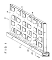
- FIG. 1 of the drawings a planar type microwave antenna structure with arrays of plate-shaped radiators for radiation/reception of circularly polarized microwaves, which is designated generally by the numeral 10.
- This antenna 10 has a rectangular slotted waveguide 12 for transmission of microwave electromagnetic energy through its interior.
- Waveguide 12 serves as a power-feed waveguide in this antenna 10, and is coupled to planar waveguide 14 serving as a radiator array waveguide.
- a plurality of rows of narrow slots 16 are formed in a matrix in the upper conductive (metallic) plate of array waveguide 14.
- the slots 16 are narrow openings or windows cut in the upper plate of waveguide 14.
- Fig. 1 illustrates slots 16 as if they were elongated rectangular areas on the plate, for the sake of simplicity.
- Metal plates (to be referred to as "patch plates” or “patch radiators” hereinafter) 18 for radiating and receiving circularly polarized microwaves are respectively arranged on slots 16 of array waveguide 14.
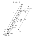
- Feed waveguide 12 is constituted by a hollow rectangular metal pipe having width b f and height h f , as illustrated in Fig. 2 in detail.
- One end 12a of waveguide 12 is open to serve as a feed end, and the other end 12b thereof is closed, i.e., short-circuited.
- Waveguide 12 transmits a TE01 mode microwave along its longitudinal direction as indicated by arrow 20.
- a broadside array of slots 22-1, 22-2,..., 22-n (the suffixes "1", “2",..., “n” will be dropped if there is no need to distinguish them from each other in the following description) are formed in one side surface (known as an H surface) of waveguide 12.
- the centers of successive slots 22 are spaced a half guide wavelength ⁇ gf apart as shown in Fig. 2 as " ⁇ gf /2".
- the TE01 mode microwave input to waveguide 12 through feed end 12a propagates through slots 22 toward the inside of planar waveguide 14 with patch array 18.
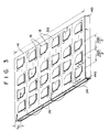
- Array waveguide 14 is constituted by a wide, thin, rectangular metal tube having width b a and height h0, as illustrated in Fig. 3 in detail. Coupling end portion 14a of array waveguide 14 is open as shown in Fig. 3, and end portion 14b opposite thereto is completely closed, i.e., short-circuited. Microwaves transmitted from slots 22 of waveguide 12 through open end portion 14a of waveguide 14 propagate toward closed end portion 14b as a TE 0n mode (higher mode) microwave.
- Array waveguide 14 is equivalently considered to be divided into a plurality of rows of rectangular waveguide components by electric walls (parallel to the propagating direction of microwaves in waveguide 14) indicated by broken lines 26 in Fig. 3.
- the width of each waveguide component row corresponds to a wavelength half a guide wavelength ( ⁇ ga ) (i.e., ⁇ ga /2). Therefore, waveguide 14 is equivalent to an arrangement in which a plurality of (n) rectangular waveguide components, each having width ⁇ ga /2 and height h0 are aligned parallel to each other.
- the phases of TE06 mode microwaves propagating through the two adjacent rectangular waveguide components are shifted through 180° from each other, as can be understood from solid sin curve 24 indicating the TE06 mode microwave in Fig. 3. This is associated with the positions of narrow slots 16 formed in waveguide 14 and the excitation phases of patch radiators 18.
- Each row of narrow slots 16, i.e., narrow slots 16 formed in each rectangular waveguide component are aligned in a zigzag manner.
- alternate slots 16 are on opposite sides of the center line of the upper surface of each waveguide component, and the distance between the opposing slots is constant.
- the zigzag patterns of the two neighbouring rows of slots 16 are line-symmetrical with each other. Therefore, slots 16 on the two waveguide components neighbouring through electric wall 26 are arranged in a mirror-like manner, as illustrated in Fig. 3.
- a pitch between slots 16 in the microwave propagating direction of each row of narrow slots 16 is selected to be half the guide wavelength ( ⁇ ga ) (i.e., ⁇ ga /2).
- Patch radiators 18 are arranged on array waveguide 14 to be coupled to the corresponding slots 16 arranged in the zigzag manner, thereby forming a two-dimensional radiator array.
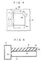
- the coupling condition between slot 16 and patch radiator 18 is apparent from the partial plan view of waveguide 14 in Fig. 4.
- patch radiator 18 is constituted by a W ⁇ L rectangular thin metal plate.
- the size of all the slots 16 is the same and that of all the radiators 18 is also the same.
- Patch radiator 18 is arranged to partially overlap the corresponding slot 16.
- a triangular chip portion, in which the length of each of two sides forming a right angle therebetween is a is cut from rectangular patch radiator 18.
- the coupling condition between slot 16 and patch radiator 18 changes depending on the overlapping area therebetween. Referring to Fig. 4, slot 16 and radiator 18 overlap each other by an area half the width of slot 16.
- Fig. 5 is a partial sectional view of the antenna of this embodiment, best showing the coupling condition between slot 16 and patch radiator 18 of waveguide 14 (not drawn to scale).
- Fig. 5 best illustrates a state wherein waveguides 12 and 14 are coupled through slots 22.
- Patch radiators 18 are arranged on insulative layer 30 (layer 30 is omitted from Figs. 1, 3 and 4 for the sake of simplicity) formed on the upper surface of waveguide 14 to satisfy the overlap condition with slots 16.
- patch radiator 18 arrays are formed by using pattern-printed board 32 sandwiching insulative layer (or insulative substrate) 30 between two, upper and lower metal plate layers. More specifically, when the metal plate layers on pattern-printed board 32 are etched by a known photolithography technique, slot 16 arrays and patch radiator 18 arrays can be easily formed on two surfaces of board 32 with high precision.
- the side walls and the bottom portion of waveguide 14 can be realized by mounting appropriate metal plates by, e.g., welding.
- patch radiators 18 are aligned on waveguide 14 so that their cutaway portions 18a are alternately directed in different directions.
- This alignment of radiators 18 is necessary for obtaining the same rotational direction of circularly polarized microwaves radiated from radiators 18 and for cophasing them.
- the pitch in each row of slots 16 is selected to be half guide wavelength ⁇ ga (i.e., ⁇ ga /2), and cutaway portions 18a of radiators 18 are alternately directed in different directions rotated through 180°.
- the circularly polarized microwaves radiated from radiators 18 are cophased in a direction perpendicular to the patch radiator alignment surface of waveguide 14, and are correctly rotated in the same direction.
- each row of patch radiator array i.e., patch radiators 18 aligned in the axial direction of each equivalent rectangular waveguide component
- each row of patch radiator array is arranged such that their cutaway portions 18a are alternately directed in different directions rotated through 180°. Since the above patch radiator alignment is adopted, circularly polarized microwaves, which are rotated in the same direction and are cophased, can be radiated from the radiators of the antenna of this embodiment.
- the excitation amplitudes of the circularly polarized microwaves from radiators 18 have a uniform distribution or a tapered distribution, as well as they are rotated in the same direction and are cophased.
- the distribution of the excitation amplitudes can be determined by a distance indicated by x in Fig. 3 (i.e., a distance between the axial center of each rectangular waveguide component and the center of slot 16). For example, if distance x increases, the excitation amplitude increases. On the contrary, if distance x increases, patch radiators 18 are not aligned in a line but arranged in a zigzag form. This technique can be applied to adjust the coupling from slots 22 of waveguide 12 to 14.
- the planar antenna when a circularly polarized microwave is radiated, no wire lines or no microstrip lines are used for propagating microwaves from a microwave source to patch radiators 18. More specifically, microwave propagation to waveguide 14 is performed by waveguide 12. Microwave propagation between slots 16 and radiators 18 of waveguide 14 is performed through thin insulative layer 30. In other words, radiators 18 are excited directly by slots 16. Therefore, a microwave loss during power feeding can be minimized, thereby improving the aperture efficiency of the antenna. For example, when power is fed through wire lines, a 12-GHz microwave is attenuated by about 4 dB per 1-m wire line. In contrast to this, when waveguide 12 is used, the microwave attenuation rate is very low (i.e., about 0.1 dB/m).
- the generation of grating lobes in a radiation pattern of the circularly polarized microwave can be satisfactorily suppressed without using a slow-wave circuit necessary in the conventional radial-line slot-array type planar antenna.
- the reason for this is as follows.
- Special-purpose patch radiators 18 are provided to the corresponding slots 16 formed in waveguide 14. With this arrangement, in order to suppress the generation of grating lobes, an alignment spacing between radiators must be minimized since the generation of grating lobes depends on this spacing.
- two open boundary planes 18b and 18c perpendicular to slot 16 act as a local radiator.
- the distance between the open boundary planes serving as the local radiator extending perpendicular to narrow slots 16 can be smaller than free-space wavelength ⁇ 0 (the present inventors confirmed a case wherein it was decreased to 0.7 ⁇ 0) with respect to the whole radiator array shown in Fig. 1.
- the same argument may be also applied to the distance between open boundary planes extending parallel with narrow slots 16.
- the alignment spacing of the radiators of the antenna can be effectively decreased, and the generation of grating lobes can be suppressed.
- a well circularly polarized microwave having an excellent directivity can be obtained at a maximum efficiency without requiring any additional circuitry (e.g., a slow-wave circuit).
- the present inventors prepared a 14-element antenna having the basic arrangement shown in Fig. 1.
- width b a and height h0 of array waveguide 14 were respectively set to be 17.677 mm, and 10 mm.
- width d and length l were respectively set to be 0.2 mm and 7.1 mm, and distance x from the central axis of each rectangular waveguide component was set to be 8.3 mm.
- a test operation was conducted using this antenna, and its aperture efficiency, radiation pattern and axial ratio were measured.
- the measured radiation pattern of right circularly polarized wave is as shown in Fig. 6.
- the axis ratio was measured to be 0.5 dB, which shows an excellent circularly polarized microwave characteristic.
- each patch radiator 18 is excited directly by the corresponding slot 16 through insulative layer 30, the coupling condition between slots 16 and radiators 18 on waveguide 14 can be accurately set, and the manufacture of waveguide 14 can be simplified. This is because the insulative substrate sandwiched between two metal layers can be etched by photolithography to form alignment patterns of slots 16 and patch radiators 18 at the same time. Therefore, the mounting step of patch radiators 18 on waveguide 14, which is necessary in the conventional planar antenna, can be omitted. This means a high-performance antenna can be realized with a low manufacturing cost, resulting in great practical advantages for antenna manufacturers.
- FIG. 7 A planar antenna according to a second embodiment of the present invention will now be described with reference to Fig. 7.
- rectangular waveguide 52 serving as a power-feed waveguide is coupled to the lower plate of wide, thin planar waveguide 54, which has a plurality of rows of narrow slots 16 and patch radiators 18 electromagnetically coupled thereto.
- Planar waveguide 54 has no open end face. In this case, microwave propagation between waveguides 52 and 54 is performed through a row of narrow slots 56 cut in the lower plate of waveguide 54.
- the number of slots 56 is the same as that of equivalent parallel waveguide components divided by electric walls in array waveguide 54, as in the first embodiment shown in Fig. 1.
- Waveguide 52 is open at its one end portion, and is closed (i.e., short-circuited) at the other end portion thereof.
- Fig. 7 illustrates power-feed waveguide 52 which has six microwave supply slots 56 in one surface thereof.
- Array waveguide 54 also has slots 58 in its lower plate corresponding in number to slots 56. Slots 58 are arranged to coincide with slots 56.
- the coupling condition between a corresponding pair of slots 56 and 58 is best illustrated in the partial sectional view of Fig. 8. Therefore, a microwave supplied from microwave supply end 52a of waveguide 52 is guided to the inside of waveguide 54 through each pair of slots 56 and 58.
- waveguide 54 incorporates reflection plate 60, thus effectively allowing the microwave to propagate between waveguides 52 and 54.
- reflection plate 60 is mounted inside waveguide 54 to oppose the array of slots 58 and to be inclined at about 45° with respect to the inner edge of waveguide 54.
- Insulative layer 62 having a honeycomb structure is arranged to cover slots 16 formed in the upper plate of waveguide 54 in the same manner as in the first embodiment.
- Patch radiators 18 are arranged on the surface of insulative layer 62 opposite slots 16 to be excited directly by the corresponding slots 16.
- the electromagnetical coupling condition between slots 16 and patch radiator 18 is the same as in the first embodiment.
- the outer shape of the slot antenna can be compact without impairing the effect of the present invention, which provides an improvement of the basic characteristics of the antenna (i.e., an improvement of an aperture efficiency and a microwave directivity). Since insulative layer 62 interposed between slots 16 and patch radiators 18 has a honeycomb structure, a dielectric loss in microwave propagation can be reduced.
- patch radiators 18 are aligned on the waveguide to be directed in the same direction.
- waveguide 54 on which a plurality of rows of patch radiators 18 are formed is divided by electric walls 26 into a plurality of equivalent parallel rectangular waveguide components. Some or all of these electric walls can be replaced with metal partition plates. With this arrangement, the mechanical strength of wide, thin waveguide 14 or 54 can be improved.
Landscapes
- Physics & Mathematics (AREA)
- Electromagnetism (AREA)
- Waveguide Aerials (AREA)
- Variable-Direction Aerials And Aerial Arrays (AREA)
Claims (9)
- Planarantennenaufbau, umfassend eine Mikrowellen-Speiseneinrichtung zum Übertragen eines Mikrowellensignals, und einer Antenneneinrichtung zum Abstrahlen des Mikrowellensignals in den Raum, wobei die Mikrowellen-Speiseneinrichtung einen ersten geschlitzten Wellenleiter (12, 52) aufweist und die Antenneneinrichtung einen zweiten geschlitzten Wellenleiter (14, 54) besitzt, der mit dem ersten geschlitzten Wellenleiter gekoppelt ist, wobei der zweite geschlitzte Wellenleiter eine leitende Platte enthält, in welcher ein zwei-dimensionales Schlitz-Feld mit mehreren Reihen von Schlitzen (16) gebildet ist, dadurch gekennzeichnet, daß auf der leitenden Platte zum Abdecken des zwei-dimensionalen Schlitz-Feldes eine Isolierschicht (30, 62) vorgesehen ist, und mehrere Reihen von plattenförmigen Radiatoren (18) elektromagnetisch mit den Schlitzen (16) jeweils derart gekoppelt sind, daß jeder Radiator (18) den entsprechenden Schlitz (16) an einem Randabschnitt von ihm teilweise überlappt und direkt von dem entsprechenden Schlitz (16) über die Isolierschicht (30, 62) erregt wird, um dadurch eine kreispolarisierte Mikrowelle abzustrahlen.
- Antennenaufbau nach Anspruch 1, dadurch gekennzeichnet, daß die Radiatoren in jedem Radiatorfeld zwei Kanten aufweisen, die im wesentlichen senkrecht zu ihrem Überlappungskantenabschnitt verlaufen und offenen Grenzebenen (18b, 18c) entsprechen, die als lokale Radiatoren dienen und daß der Abstand zwischen den offenen Grenzebenen (18b, 18c) jedes Radiators (18) so eingestellt ist, daß er kleiner ist als eine Freiraum-Wellenlänge (λ₀), um so die Erzeugung von Gitterkeulen im Strahlungsmuster der Antenne (10, 50) zu unterdrücken.
- Antenne nach Anspruch 1 oder 2, dadurch gekennzeichnet, daß die Radiatoren rechtwinklige leitenden Platten (18) aufweisen, von denen jede an seinem einen Kantenabschnitt einen weggeschnittenen Abschnitt (18a) besitzt.
- Antenne nach Anspruch 3, dadurch gekennzeichnet, daß der zweite geschlitzte Wellenleiter durch mindestens eine elektrische Wand (26) in parallele Wellenleiterkomponenten unterteilt ist, die jeweils ein Feld von plattenförmigen Radiatoren besitzen.
- Antenne nach Anspruch 3, dadurch gekennzeichnet, daß der zweite geschlitzte Wellenleiter (14) eine offene Seitenfläche (14a) senkrecht zu den Reihen von Schlitzen (16) besitzt, und daß der erste geschlitzte Wellenleiter (12) ein Feld von zweiten Schlitzen (22) besitzt, die entlang einer Mikrowellen-Ausbreitungsrichtung des Wellenleiters in einer Seitenfläche ausgerichtet sind, die mit der offenen Seitenfläche (14a) des zweiten geschlitzten Wellenleiters 814) gekoppelt ist, wodurch eine Mikrowellenausbreitung zwischen dem ersten und dem zweiten geschlitzten Wellenleiter (12, 14) über die zweiten Schlitze (22) erfolgt.
- Antenne nach Anspruch 3, dadurch gekennzeichnet, daß der zweite geschlitzte Wellenleiter (54) ein Feld von zweiten Schlitzen (58) in einer Seitenfläche von ihm besitzt, und daß der erste geschlitzte Wellenleiter (52) ein Feld von dritten Schlitzen (56) besitzt, die den zweiten Schlitzen (58) entsprechen und entlang einer Mikrowellen-Ausbreitungsrichtung in dem Wellenleiter in einer Seitenfläche von ihm, die mit dem zweiten geschlitzten Wellenleiter (54) gekoppelt ist, ausgerichtet sind, wodurch eine Mikrowellen-Ausbreitung zwischen dem ersten und dem zweiten geschlitzten Wellenleiter (52, 54) über die miteinander gekoppelten zweiten und dritten Schlitze (56, 58) erfolgt.
- Antenne nach Anspruch 6, dadurch gekennzeichnet, daß der zweite geschlitzte Wellenleiter (54) eine zweite leitende Platte besitzt, die von der leitenden Platte, auf der die Isolierschicht gebildet ist, unter Bildung einer Lücke beabstandet ist, und in der die dritten Schlitze (58) ausgebildet sind, und einer Reflektoreinrichtung (60) aufweist, die im Inneren des zweiten geschlitzten Wellenleiters derart festgelegt ist, daß sie den dritten Schlitzen (58) gegenüberliegt und bezüglich der zweiten leitenden Platte geneigt ist, und die eine in einer Richtung empfangene Mikrowelle so reflektiert, daß sie sich in die andere Richtung zwischen dem ersten und dem zweiten geschlitzten Wellenleiter (52, 54) fortpflanzt.
- Antennenaufbau nach einem der Ansprüche 1 bis 7, dadurch gekennzeichnet, daß die Länge ("1" in Fig. 4) des entsprechenden Schlitzes (16) größer ist als diejenige (w) der dazugehörigen Kante jedes Radiators (18).
- Herstellungsverfahren für eine Planarantenne mit Streifenradiatoren zum Aussenden von kreispolarisierten Mikrowellen in den Raum, umfassend die Schritte:
Ausbilden einer ersten und einer zweiten leitenden Platte auf beiden Flächen eines isolierenden Substrats (30, 62);
Ätzen der ersten und der zweiten leitenden Platte mittels Fotolithographie, um ein zwei-dimensionales Schlitzfeld mit mehreren Reihen von Schlitzen (16) in der ersten leitenden Platte auszubilden und um in der zweiten leitenden Platte mehrere Reihen von plattenförmigen Streifenradiatoren (18) auszubilden, die mit den entsprechenden Schlitzen (16) derart elektromagnetisch gekoppelt sind, daß jeder Radiator (18) direkt von dem entsprechenden Schlitz (16) durch das isolierende Substrat (30, 62) erregt wird und dadurch eine kreispolarisierte Mikrowelle abstrahlt;
Anbringen eines leitenden Hüllkörpers an der geätzten ersten leitenden Platte, um so einen Planar-Feld-Wellenleiter (14, 54) zu erhalten; und
Koppeln eines Leistungs-Speiseschlitz-Wellenleiters (12, 52) an den Feld-Wellenleiter, um dem Feld-Wellenleiter eine Mikrowelle zuzuführen.
Applications Claiming Priority (2)
| Application Number | Priority Date | Filing Date | Title |
|---|---|---|---|
| JP60158366A JPS6220403A (ja) | 1985-07-19 | 1985-07-19 | スロツト給電アレイアンテナ |
| JP158366/85 | 1985-07-19 |
Publications (3)
| Publication Number | Publication Date |
|---|---|
| EP0209156A2 EP0209156A2 (de) | 1987-01-21 |
| EP0209156A3 EP0209156A3 (en) | 1988-02-24 |
| EP0209156B1 true EP0209156B1 (de) | 1991-12-18 |
Family
ID=15670112
Family Applications (1)
| Application Number | Title | Priority Date | Filing Date |
|---|---|---|---|
| EP86109904A Expired EP0209156B1 (de) | 1985-07-19 | 1986-07-18 | Planarantenne mit Streifenradiator |
Country Status (5)
| Country | Link |
|---|---|
| US (1) | US4755821A (de) |
| EP (1) | EP0209156B1 (de) |
| JP (1) | JPS6220403A (de) |
| CA (1) | CA1261060A (de) |
| DE (1) | DE3682962D1 (de) |
Families Citing this family (52)
| Publication number | Priority date | Publication date | Assignee | Title |
|---|---|---|---|---|
| JPS6457804A (en) * | 1987-08-27 | 1989-03-06 | Naohisa Goto | Circular waveguide line |
| JPH0629522Y2 (ja) * | 1987-12-08 | 1994-08-10 | 三菱重工業株式会社 | 流体圧シリンダユニツト |
| US4843400A (en) * | 1988-08-09 | 1989-06-27 | Ford Aerospace Corporation | Aperture coupled circular polarization antenna |
| GB2226703A (en) * | 1988-12-16 | 1990-07-04 | Marconi Co Ltd | Antenna |
| JP2641944B2 (ja) * | 1989-07-07 | 1997-08-20 | 株式会社 新興製作所 | 進行波給電式同軸スロットアンテナ |
| GB2236907B (en) * | 1989-09-20 | 1994-04-13 | Beam Company Limited | Travelling-wave feeder type coaxial slot antenna |
| GB2238914B (en) * | 1989-11-27 | 1994-05-04 | Matsushita Electric Works Ltd | Waveguide feeding array antenna |
| US4985708A (en) * | 1990-02-08 | 1991-01-15 | Hughes Aircraft Company | Array antenna with slot radiators offset by inclination to eliminate grating lobes |
| GB2244381A (en) * | 1990-05-23 | 1991-11-27 | Philips Electronic Associated | Microstrip patch antenna |
| CA2059364A1 (en) * | 1991-01-30 | 1992-07-31 | Eric C. Kohls | Waveguide transition for flat plate antenna |
| US5241321A (en) * | 1992-05-15 | 1993-08-31 | Space Systems/Loral, Inc. | Dual frequency circularly polarized microwave antenna |
| KR0147035B1 (ko) * | 1993-07-31 | 1998-08-17 | 배순훈 | 개선된 헤리컬 와이어 배열 평면안테나 |
| FR2729011B1 (fr) * | 1994-12-28 | 1997-01-31 | Le Centre Thomson D Applic Rad | Antenne reseau a double polarisation et a faibles pertes |
| US5661494A (en) * | 1995-03-24 | 1997-08-26 | The United States Of America As Represented By The Administrator Of The National Aeronautics And Space Administration | High performance circularly polarized microstrip antenna |
| GB9513936D0 (en) * | 1995-07-07 | 1996-04-24 | Gec Marconi Avionics Holdings | Radar apparatus |
| JPH1051228A (ja) * | 1996-08-05 | 1998-02-20 | Nippon Telegr & Teleph Corp <Ntt> | アンテナ装置 |
| US6297774B1 (en) | 1997-03-12 | 2001-10-02 | Hsin- Hsien Chung | Low cost high performance portable phased array antenna system for satellite communication |
| US5818391A (en) * | 1997-03-13 | 1998-10-06 | Southern Methodist University | Microstrip array antenna |
| SE509448C2 (sv) * | 1997-05-07 | 1999-01-25 | Ericsson Telefon Ab L M | Dubbelpolariserad antenn samt enkelpolariserat antennelement |
| US5896107A (en) * | 1997-05-27 | 1999-04-20 | Allen Telecom Inc. | Dual polarized aperture coupled microstrip patch antenna system |
| US6002368A (en) * | 1997-06-24 | 1999-12-14 | Motorola, Inc. | Multi-mode pass-band planar antenna |
| US5933115A (en) * | 1997-06-06 | 1999-08-03 | Motorola, Inc. | Planar antenna with patch radiators for wide bandwidth |
| WO1999034477A1 (en) * | 1997-12-29 | 1999-07-08 | Hsin Hsien Chung | Low cost high performance portable phased array antenna system for satellite communication |
| JP2001339207A (ja) * | 2000-05-26 | 2001-12-07 | Kyocera Corp | アンテナ給電線路およびそれを用いたアンテナモジュール |
| US6313807B1 (en) * | 2000-10-19 | 2001-11-06 | Tyco Electronics Corporation | Slot fed switch beam patch antenna |
| US6896582B2 (en) | 2000-12-20 | 2005-05-24 | With Kabushiki Kaisha | Clothing for woman |
| DE10131283A1 (de) * | 2001-06-28 | 2003-01-09 | Philips Corp Intellectual Pty | Phased Array Antenne |
| GB0127772D0 (en) * | 2001-11-20 | 2002-01-09 | Smiths Group Plc | Antennas |
| KR100506481B1 (ko) * | 2002-08-06 | 2005-08-08 | 한국전자통신연구원 | 혼합 급전 방식을 이용한 마이크로스트립 배열 안테나 |
| US7127255B2 (en) * | 2002-10-01 | 2006-10-24 | Trango Systems, Inc. | Wireless point to multipoint system |
| US6894582B2 (en) | 2003-02-07 | 2005-05-17 | Harris Corporation | Microwave device having a slotted coaxial cable-to-microstrip connection and related methods |
| RU2258285C1 (ru) * | 2003-11-21 | 2005-08-10 | Самсунг Электроникс Ко., Лтд. | Планарная антенна |
| JP4029217B2 (ja) * | 2005-01-20 | 2008-01-09 | 株式会社村田製作所 | 導波管ホーンアレイアンテナおよびレーダ装置 |
| JP2007027894A (ja) * | 2005-07-12 | 2007-02-01 | Omron Corp | 広帯域アンテナおよび広帯域アンテナ搭載基板 |
| JP5173810B2 (ja) * | 2006-08-11 | 2013-04-03 | 古野電気株式会社 | スロットアレイアンテナ |
| US7498994B2 (en) * | 2006-09-26 | 2009-03-03 | Honeywell International Inc. | Dual band antenna aperature for millimeter wave synthetic vision systems |
| US7724176B1 (en) | 2009-03-13 | 2010-05-25 | Raytheon Company | Antenna array for an inverse synthetic aperture radar |
| WO2012167283A2 (en) | 2011-06-02 | 2012-12-06 | Brigham Young University | Planar array feed for satellite communications |
| US9112262B2 (en) | 2011-06-02 | 2015-08-18 | Brigham Young University | Planar array feed for satellite communications |
| JP5939690B2 (ja) * | 2013-07-31 | 2016-06-22 | 日本電信電話株式会社 | 一次元スロットアレーアンテナ |
| JP5936644B2 (ja) * | 2014-04-11 | 2016-06-22 | 三菱電機株式会社 | 導波管給電パッチアレーアンテナ装置 |
| JP6396244B2 (ja) | 2015-03-25 | 2018-09-26 | パナソニック株式会社 | レーダ装置 |
| JP6786084B2 (ja) * | 2017-01-23 | 2020-11-18 | 国立研究開発法人産業技術総合研究所 | レーダアンテナ |
| US11652301B2 (en) | 2018-04-11 | 2023-05-16 | Qualcomm Incorporated | Patch antenna array |
| KR20200133767A (ko) | 2018-04-19 | 2020-11-30 | 메타웨이브 코포레이션 | 안테나 어레이 소자의 방사 방법 및 장치 |
| CN114616721B (zh) * | 2019-10-21 | 2025-09-26 | 株式会社村田制作所 | 圆极化阵列天线装置 |
| CN111326852A (zh) * | 2020-02-28 | 2020-06-23 | 西南电子技术研究所(中国电子科技集团公司第十研究所) | 低剖面二维宽角扫描圆极化相控阵天线 |
| CN111883938B (zh) * | 2020-07-31 | 2022-06-14 | 广州程星通信科技有限公司 | 一种单馈点阵列组合相控阵天线 |
| CN112736436B (zh) * | 2020-12-18 | 2024-10-15 | 中国电子科技集团公司第五十四研究所 | 一种阵列天线 |
| CN114956248B (zh) * | 2021-02-24 | 2023-08-22 | 陕西青朗万城环保科技有限公司 | 一种狭缝微波辐射器 |
| CN116706566B (zh) * | 2023-07-19 | 2024-02-09 | 石家庄锐创电子科技有限公司 | 一种法布里-珀罗腔结构式大间距相控阵天线 |
| CN117594969B (zh) * | 2024-01-19 | 2024-04-02 | 微网优联科技(成都)有限公司 | 一种新型谐振器结构及方向图可重构天线 |
Family Cites Families (6)
| Publication number | Priority date | Publication date | Assignee | Title |
|---|---|---|---|---|
| US2479209A (en) * | 1945-07-09 | 1949-08-16 | Chu Lan Jen | Antenna |
| GB1502943A (en) * | 1975-05-09 | 1978-03-08 | Cary R | Microwave antennas |
| US4213133A (en) * | 1977-11-10 | 1980-07-15 | Tokyo Shibaura Denki Kabushiki Kaisha | Linear antenna arrays |
| JPS57142002A (en) * | 1981-02-27 | 1982-09-02 | Toshiba Corp | Small-sized loop antenna |
| JPS58123206A (ja) * | 1982-01-19 | 1983-07-22 | Mitsubishi Electric Corp | 導波管形スロツトアレイアンテナ |
| JPH0682970B2 (ja) * | 1985-01-09 | 1994-10-19 | 株式会社東芝 | 円偏波一次放射器 |
-
1985
- 1985-07-19 JP JP60158366A patent/JPS6220403A/ja active Pending
-
1986
- 1986-07-18 US US06/886,676 patent/US4755821A/en not_active Expired - Lifetime
- 1986-07-18 EP EP86109904A patent/EP0209156B1/de not_active Expired
- 1986-07-18 CA CA000514191A patent/CA1261060A/en not_active Expired
- 1986-07-18 DE DE8686109904T patent/DE3682962D1/de not_active Expired - Lifetime
Also Published As
| Publication number | Publication date |
|---|---|
| EP0209156A2 (de) | 1987-01-21 |
| EP0209156A3 (en) | 1988-02-24 |
| CA1261060A (en) | 1989-09-26 |
| DE3682962D1 (de) | 1992-01-30 |
| JPS6220403A (ja) | 1987-01-29 |
| US4755821A (en) | 1988-07-05 |
Similar Documents
| Publication | Publication Date | Title |
|---|---|---|
| EP0209156B1 (de) | Planarantenne mit Streifenradiator | |
| US10879616B2 (en) | Shared-aperture antenna | |
| EP0329079B1 (de) | Antenne mit geschlitztem Hohlleiter | |
| US4401988A (en) | Coupled multilayer microstrip antenna | |
| EP0142555B1 (de) | Doppelbandige phasengesteuerte antennengruppe mit breitbandigem element und diplexer | |
| KR0184529B1 (ko) | 슬롯 안테나 및 원편파 에너지 수신 방법 | |
| US6166701A (en) | Dual polarization antenna array with radiating slots and notch dipole elements sharing a common aperture | |
| US4743915A (en) | Four-horn radiating modules with integral power divider/supply network | |
| US6731241B2 (en) | Dual-polarization common aperture antenna with rectangular wave-guide fed centered longitudinal slot array and micro-stripline fed air cavity back transverse series slot array | |
| EP0410083B1 (de) | Ringschlitzantenne | |
| US2914766A (en) | Three conductor planar antenna | |
| US20020067315A1 (en) | Aperture coupled slot array antenna | |
| EP1018778B1 (de) | Mehrschichtige Streifenleiterantenne | |
| CN113659325B (zh) | 集成基片间隙波导阵列天线 | |
| EP0067573B1 (de) | Antennegruppen | |
| US3509572A (en) | Waveguide fed frequency independent antenna | |
| US7436371B1 (en) | Waveguide crescent slot array for low-loss, low-profile dual-polarization antenna | |
| US6781554B2 (en) | Compact wide scan periodically loaded edge slot waveguide array | |
| EP0542447B1 (de) | Ebene Plattenantenne | |
| US5070339A (en) | Tapered-element array antenna with plural octave bandwidth | |
| Hall et al. | Survey of design techniques for flat profile microwave antennas and arrays | |
| WO1996010277A9 (en) | Planar high gain microwave antenna | |
| JPH0548323A (ja) | 2偏波共用アンテナ | |
| US5426441A (en) | Planar slot antenna grid | |
| JPH05160626A (ja) | 無給電素子付きトリプレート型平面アンテナ |
Legal Events
| Date | Code | Title | Description |
|---|---|---|---|
| PUAI | Public reference made under article 153(3) epc to a published international application that has entered the european phase |
Free format text: ORIGINAL CODE: 0009012 |
|
| AK | Designated contracting states |
Kind code of ref document: A2 Designated state(s): DE FR GB |
|
| PUAL | Search report despatched |
Free format text: ORIGINAL CODE: 0009013 |
|
| AK | Designated contracting states |
Kind code of ref document: A3 Designated state(s): DE FR GB |
|
| 17P | Request for examination filed |
Effective date: 19880209 |
|
| 17Q | First examination report despatched |
Effective date: 19900123 |
|
| GRAA | (expected) grant |
Free format text: ORIGINAL CODE: 0009210 |
|
| AK | Designated contracting states |
Kind code of ref document: B1 Designated state(s): DE FR GB |
|
| REF | Corresponds to: |
Ref document number: 3682962 Country of ref document: DE Date of ref document: 19920130 |
|
| ET | Fr: translation filed | ||
| PLBE | No opposition filed within time limit |
Free format text: ORIGINAL CODE: 0009261 |
|
| STAA | Information on the status of an ep patent application or granted ep patent |
Free format text: STATUS: NO OPPOSITION FILED WITHIN TIME LIMIT |
|
| 26N | No opposition filed | ||
| REG | Reference to a national code |
Ref country code: GB Ref legal event code: 746 Effective date: 19981015 |
|
| REG | Reference to a national code |
Ref country code: FR Ref legal event code: D6 |
|
| REG | Reference to a national code |
Ref country code: GB Ref legal event code: IF02 |
|
| PG25 | Lapsed in a contracting state [announced via postgrant information from national office to epo] |
Ref country code: FR Free format text: LAPSE BECAUSE OF NON-PAYMENT OF DUE FEES Effective date: 20040331 |
|
| REG | Reference to a national code |
Ref country code: FR Ref legal event code: ST |
|
| REG | Reference to a national code |
Ref country code: FR Ref legal event code: RN Ref country code: FR Ref legal event code: D3 |
|
| PGFP | Annual fee paid to national office [announced via postgrant information from national office to epo] |
Ref country code: FR Payment date: 20050708 Year of fee payment: 20 |
|
| PGFP | Annual fee paid to national office [announced via postgrant information from national office to epo] |
Ref country code: GB Payment date: 20050713 Year of fee payment: 20 |
|
| PGFP | Annual fee paid to national office [announced via postgrant information from national office to epo] |
Ref country code: DE Payment date: 20050714 Year of fee payment: 20 |
|
| PG25 | Lapsed in a contracting state [announced via postgrant information from national office to epo] |
Ref country code: GB Free format text: LAPSE BECAUSE OF EXPIRATION OF PROTECTION Effective date: 20060717 |
|
| REG | Reference to a national code |
Ref country code: GB Ref legal event code: PE20 |