EP0209252A2 - Detektor für kleine Fehlstellen in gedruckten Schaltungskarten - Google Patents
Detektor für kleine Fehlstellen in gedruckten Schaltungskarten Download PDFInfo
- Publication number
- EP0209252A2 EP0209252A2 EP86304620A EP86304620A EP0209252A2 EP 0209252 A2 EP0209252 A2 EP 0209252A2 EP 86304620 A EP86304620 A EP 86304620A EP 86304620 A EP86304620 A EP 86304620A EP 0209252 A2 EP0209252 A2 EP 0209252A2
- Authority
- EP
- European Patent Office
- Prior art keywords
- bit
- pixel
- registers
- shift registers
- bits
- Prior art date
- Legal status (The legal status is an assumption and is not a legal conclusion. Google has not performed a legal analysis and makes no representation as to the accuracy of the status listed.)
- Withdrawn
Links
Images


Classifications
-
- G—PHYSICS
- G06—COMPUTING OR CALCULATING; COUNTING
- G06T—IMAGE DATA PROCESSING OR GENERATION, IN GENERAL
- G06T7/00—Image analysis
- G06T7/0002—Inspection of images, e.g. flaw detection
- G06T7/0004—Industrial image inspection
-
- G—PHYSICS
- G06—COMPUTING OR CALCULATING; COUNTING
- G06T—IMAGE DATA PROCESSING OR GENERATION, IN GENERAL
- G06T2207/00—Indexing scheme for image analysis or image enhancement
- G06T2207/10—Image acquisition modality
- G06T2207/10016—Video; Image sequence
-
- G—PHYSICS
- G06—COMPUTING OR CALCULATING; COUNTING
- G06T—IMAGE DATA PROCESSING OR GENERATION, IN GENERAL
- G06T2207/00—Indexing scheme for image analysis or image enhancement
- G06T2207/30—Subject of image; Context of image processing
- G06T2207/30108—Industrial image inspection
- G06T2207/30141—Printed circuit board [PCB]
Definitions
- a printed circuit board comprises a substrate, typically made of fiberglass or mylar whose surface has metal lines formed thereon which are electrical conductors used to connect various circuit components together and/or to external circuitry.
- metal lines formed thereon which are electrical conductors used to connect various circuit components together and/or to external circuitry.
- feature sizes i.e, lines and spaces between the metal lines have shrunk to very small dimensions, e.g., 0.005 inches.
- a certain percentage of printed circuit boards still come out of production with one or more of a variety of flaws.
- a printed circuit board may have lines and/or spaces too narrow, shorts, opens, pinholes or the like; any one of which may render the board useless. Due to the extremely small sizes involved visual detection of such flaws in boards with very fine lines is neither technically effective nor economically practical.
- automation of the printed circuit board inspection process is an essential requirement in the fast growing world of electronic circuitry.
- the present invention relates to a system for the automatic inspection of printed circuit boards and the like.
- a video camera scans the surface, e.g., the surface of a printed circuit board to be inspected for flaws such as lines and spaces too narrow, shorts, open circuits and the like in the circuit patterns formed on the surface thereof.
- the video camera which may be a charged coupled device array is periodically sensitized and emptied of its video contents with each such event constituting a scan line.
- a video processor converts each scan line of video data into a serial stream of analog levels each representative of a picture element or pixel of the surface being scanned.
- the output of the video processor is first quantized into binary data (1 or 0) according to the level of the analog signal with respect to a preset threshold.
- This data is then fed to a unique delay circuit where the data is configured into image windows of n x n bits or pixels. Each image window changes on the occurrence of each pixel clock which may occur at a 10 MH 2 rate.
- the image window provides n 2 outputs each of which is a bit representative. of the black and white levels of a pixel undergoing inspection.
- the dynamically changing n 2 outputs are provided as inputs to programmed combinational logic arrays which have been programmed in accordance with predetermined rules algorithms for each of the flaws to be detected, i.e., for each type of flaw to be detected there is an algorithm stored in the logic array which acts as the mask, which decodes the n 2 outputs for combinations which indicate a flaw in the circuit board under inspection.
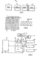
- the printed circuit inspection system 10 of the present invention comprises a video camera 11, a video processor 12, a delay circuit 13 and a flaw detector 14.
- the video camera 11 which in a practical embodiment comprises a charged couple device array hereinafter referred to as a CCD array is caused to scan relative to the surface to be inspected.
- the number of scans necessary to view the entire inspection surface is a function of the length of the array as well as the size of the surface to be inspected.
- the video camera 11 or CCD array comprises 2048 light sensitive elements arranged in a straight line and is 1.024 inches in length.
- each light sensitive element in the CCD array is about 0.0005 inches by 0.0005 inches square and is capable of resolving over its length 2048 picture elements or pixels each one of which is about 0.0005 inches by 0.0005 inches square.
- CCD arrays could, of course, be used having a greater or smaller number of light sensitive elements in longer or shorter arrays depending on the degree of resolution required and scanning swath desired.
- a CCD array must be sensitized to view a surface along its array length and then the image information transferred out for processing. To inspect a surface, this sensitization and transfer of data must occur a large number of times. For example, if one wishes to view a surface 1.024 x 1.024 inches at the highest possible resolution then a CCD array having 2048 light sensitive elements each 0.0005 inches by 0.0005 inches square would have to be sensitized at unity magnification and emptied 2048 times during the scan. Thus, in this particular example, it takes 2048 scan lines to view the entire surface. For each scan line the CCD array outputs an analog signal representative of 2048 pixels. If the' surface to be inspected exceeds 1.024 inches in width, more than one scan may be required.
- the output of video camera 11 is connected to video processor 12.
- the video processor 12 functions as an A to D converter to transform the analog signal representative of the pixels in each scan line to a digital signal comprising 0's and l's each representative of a pixel viewed by the CCD array in each scan line.
- the video processor 12 is connected to delay circuit 13.
- the delay circuit 13 functions as a serial to parallel converter and provides an n x n pixel image window output in real time.
- the image window of n x n pixels comprises n 2 bits each representative of a reflecting or non- reflecting area of the inspection surface being scanned by the CCD array.
- the image window generated in delay circuit 13 is updated by "n" new pixels or bits every pixel clock which in a practical embodiment occur at a 10 MH 2 rate. As will be explained more fully hereinbelow these image windows are generated in such a way that image windows of the entire inspection surface are provided.
- the delay circuit 13 provides a matrix of n 2 outputs which are provided as inputs to flaw detector 14.
- the flaw detector 14 comprises a programmable logic array which acts as the defect mask programmed for each type of defect desired to be detected.
- the n 2 outputs from delay line 13 are decoded by the programmable logic arrays at the 10 MB previously mentioned. When a flaw is detected, flaw detector 14 provides an output.
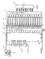
- the delay circuit 13 comprises a random access memory or RAM 15.
- the RAM 15 is 2048 x 16, i.e., it is capable of storing 16 bit words at each of 2048 addresses.
- the address counter 16 has an input from pixel clock 17 and on occurrence of each pixel clock addresses each one in succession of the 2048 memory positions of the RAM 15.
- the address counter 16 is reset at the start of each scan line by an input R which may be provided in any convenient manner, e.g., by the signal which sensitizes or unloads the CCD array.
- a transceiver 18 interconnects RAM 15 and shift registers 19.
- the shift registers comprise sixteen shift registers 19a through 19p.
- Each shift register 19a through 19p is a sixteen bit shift register with each bit position having an output.
- the shift registers 19a through 19p therefore, provide 16 x 16 or 256 outputs. These outputs are connected to programmable logic array 21 which is connected to OR circuit 22.
- Each of the shift registers 19a through 19p has a clock input from pixel clock 17 and a data input via transceiver 18 from the registers designated DO through D 15 of RAM 15,i.e., Dg is connected to shift register 19a, D 1 is connected to shift register 19 transceiver, D 2 is connected to shift register 19c etc.
- the first bit position of each of the shift registers 19a through 19p is connected via transceiver 18 to the next lower register of RAM 15, i.e., the first bit position of shift register 19a is connected to D 1 , the first bit position of shift register 19b is connected to D 2 , the first bit position of shift register 19c is connected to D 3 etc.
- Video processor 12 is connected to RAM 15 via transceiver 18 and provides a new bit of video data to the D 0 bit position of the particular one of the 2048 sixteen bit words under address in RAM 15.
- the first 16 bit word at address 1 contains the video data of the first pixel of each of the first 16 scan lines
- the second 16 bit word at address 2 contains the video data of the second pixel of each of the first 16 scan lines and so on up through the 2048th 16 bit word at address 2048.
- shift registers 19a through 19p are filled synchronously and after sixteen pixel clocks, shift registers 19a through 19b contain 16 x 16 bits of video data representative of the first sixteen pixels of each of the first sixteen scan lines. This provides an image window of 16 x 16 pixels.
- the 256 outputs, i.e., sixteen from each of the sixteen shift registers 19a through 19p are provided as inputs to programmable logic array 21 (or defect mask).
- the next word is read into shift registers 19a through 19p dumping the first word from the last bit positions, i.e., the rightmost bit position of the shift registers.
- the first 16 bit word read into shift register 19a through 19p on the first pixel clock ' consists of the first bit of the seventeenth scan line into shift register 19a, the first bit of the sixteenth scan line into shift register 19b, the first bit of the fifteenth scan line into shift register 19c etc.
- the 16 x 16 bit image window in shift registers 19a through 19p has, after one pixel clock, changed by one new bit representative of the first pixel of the seventeenth scan line in the first bit position of shift register 19a.
- the first bit of the sixteenth scan line is in the first bit position of shift register 19b, the first bit of the fifteenth scan line is in the first bit position of shift register 19c etc.
- the 16 bit word read into the shift registers 19a through 19p has one new bit in the Do position with the old bits of the word shifted down one. This occurs for each pixel clock with the word shifted in shift registers 19a through 19p being controlled by address counter 16.
- each new scan line is loaded into the Do bit positions of RAM 15 until the test surface is completely scanned.
- Each 16 x 16 bit image window being decoded by programmable logic array 21 (defect mask) changes with each pixel clock and line clock. Thus it changes by one pixel in the X-direction for each new scan line and by 16-pixels in the Y-direction for each new pixel clock.
- the 16-pixels in the Y-direction are transferred in parallel into the sixteen shift registers 19a thru 19p from the RAM 15.
- the transceiver 18 comprises sixteen each of tristate circuits 24a and 24b. On the occurrence of a pixel clock the 16 bit pixel word in the addressed bit positions of the sixteen RAM registers is transferred through 16 enabled tristate circuits like 24 into shift registers 19a through 19p by a read pulse applied to RAM 15 and the input of each of 16 circuits like 24. Then a write pulse is applied to circuit 24b and the new data bit from video processor 12 is written into the D 0 position of the 16 bit word under address in RAM 15.
- each of the sixteen shift registers and D 0 to D 15 bit positions have a similar set of circuits 24a and 24b disposed in transceiver 18 for accomplishing the foregoing described transfers between the RAM 15 and the sixteen shift registers 19a through 19p.
- the read/write pulses are essentially the pixel clock pulses.
- the address counter 16 is indexed by one and the 16 bit word stored in the first bit position of each of the sixteen 2048 bit registers of RAM 15 is shifted into the first bit position of the sixteen shift registers 19a through 19p.
- the address changes the first bit of the scan line from video processor 12'is written into the first bit position D 0 of the RAM 15.
- the bit that was in bit position Do is written into bit position D l via
- the first shift register and the bit in bit position D 1 is written into bit position D 2 via the second shift register etc. down to bit position D 15 , i.e., D 14 to D 15 with the bit originally in bit position D 15 being dumped.
- RAM 15 On each next scan the process is repeated. If the RAM 15 is originally empty it takes 16 scan lines of one bit pixel data before RAM 15 is filled. It then takes sixteen pixel clocks for the shift registers to be filled. Thereafter, at each pixel clock, the 256 bits at the outputs of the sixteen shift registers 19a through 19p change as previously described.
- n x n - pixel image window areas of the test surface under inspection are generated as previously explained in a dynamic fashion as the test surface is scanned by the video camera, i.e., CCD array 11.
- the 256 continuously changing outputs from the shift registers 19a through 19p are provided to programmable logic array 21 which has been preprogrammed according to predetermined rules algorithms to decode each image window.
- the image window changes by 16 new pixels at the pixel clock rate which in a practical embodiment is 10MH z .
- the 16-pixels in the Y-direction are transferred in parallel into the sixteen shift registers 19a thru 19p from the RAM 15.
- the image window then changes by one-pixel (a scan line) in the X-direction at the start of each new scan line.
- the number of different types of flaws being looked for may vary in number depending on the particular application.
- OR gate 22 which provides a signal to activate an alarm, e.g.,.a system interrupt, or a signal to record the event.
- the conductor lines may be too narrow or the spaces between conductor lines may be too narrow. This may be true for lines or spaces which are horizontal, vertical, diagonal or as a matter of fact any orientation. Programs can be designed for any type of flaw desired to be detected.
- Figure 4 is an example of a 10 x 10 pixel defect mask designed to detect flawed lines or spaces for horizontal orientations.
- the mask could just as easily be 16 x 16 pixel but 10 x 10 pixels has been chosen for easy presentation.
- the rejection criteria for a horizontal line or space is for line widths or' spaces less than four pixels.
- Other values could be used by appropriately programming the programmable logic array 21 which performs the defect mask function.
- the Boolean expression, i.e., combinations of Py,x needed to satisfy conditions for a horizontal line narrower than 4 pixels is:
- each square of the grid represents a pixel of 0.0005" by 0.0005".
- Relating algorithm (1) to the defect mask of Figure 4 shows that the algorithm is satisfied, i.e., a flaw exists when the expression equals 1.
- the horizontal conductor is too narrow, i.e., less than four pixels in width. In this case 0's represent the substrate and "1" represent the conductor.
- the squares of the grid which are unmarked are "don't care" values and therefore do not affect the mask expression.
- Algorithm (2) is satisfied for a flaw, i.e., spaces between horizontal conductors are too narrow by replacing the 0's with 1's and the l's with 0's in the defect mask of Figure 4.
- rejection values for a horizontal line or space too narrow can be achieved by utilizing different bit positions in the defect mask. For example,Pigure 5 will detect horizontal spaces less than 6 pixels and figure 6 will detect horizontal spaces less than 8 pixels. complementing the bits in the defect mask will enable detection of horizontal lines too narrow as previously stated.
- FIG. 9 A configuration for detecting a diagonal space which is less than 8 bits wide is shown in Figure 9. Once again, complementing the bits will detect diagonal lines less than 8 bits, changing the bit positions will enable detection of different values of rejection criteria and rotation of the bit pattern will enable detection of defects in lines orientated diagonally opposite to the configuration shown. See, for example, Figure 10 which is for diagonal spaces less than 4 pixels.
- Incipient opens and shorts can be detected using a bit pattern as shown in Figure 11 for an incipient open (in a vertical feature) or incipient short (between horizontal features) less than 4 pixels.
- bit pattern as shown in Figure 11 for an incipient open (in a vertical feature) or incipient short (between horizontal features) less than 4 pixels.
- a programmable logic array such as programmable logic array 21 may have any number of such algorithms hardwired therein and may function as a defect mask in accordance with the present invention to decode the image windows generated by the apparatus of Figure 2 to decode each image window generated for any desired flaw.
Landscapes
- Engineering & Computer Science (AREA)
- Quality & Reliability (AREA)
- Computer Vision & Pattern Recognition (AREA)
- Physics & Mathematics (AREA)
- General Physics & Mathematics (AREA)
- Theoretical Computer Science (AREA)
- Investigating Materials By The Use Of Optical Means Adapted For Particular Applications (AREA)
- Image Analysis (AREA)
- Closed-Circuit Television Systems (AREA)
- Length Measuring Devices By Optical Means (AREA)
Applications Claiming Priority (2)
| Application Number | Priority Date | Filing Date | Title |
|---|---|---|---|
| US74596685A | 1985-07-15 | 1985-07-15 | |
| US745966 | 1985-07-15 |
Publications (2)
| Publication Number | Publication Date |
|---|---|
| EP0209252A2 true EP0209252A2 (de) | 1987-01-21 |
| EP0209252A3 EP0209252A3 (de) | 1988-09-21 |
Family
ID=24998984
Family Applications (1)
| Application Number | Title | Priority Date | Filing Date |
|---|---|---|---|
| EP86304620A Withdrawn EP0209252A3 (de) | 1985-07-15 | 1986-06-16 | Detektor für kleine Fehlstellen in gedruckten Schaltungskarten |
Country Status (3)
| Country | Link |
|---|---|
| EP (1) | EP0209252A3 (de) |
| JP (1) | JPS6249204A (de) |
| IL (1) | IL79098A0 (de) |
Cited By (6)
| Publication number | Priority date | Publication date | Assignee | Title |
|---|---|---|---|---|
| GB2204170A (en) * | 1987-03-18 | 1988-11-02 | Strahlen Umweltforsch Gmbh | Real time object recognition method |
| EP0296516A3 (en) * | 1987-06-20 | 1989-11-29 | Ralf A. Sood | Signs and objects recognition process |
| EP0343664A3 (en) * | 1988-05-27 | 1990-08-29 | Kirin Beer Kabushiki Kaisha | Apparatus for detecting defects on bottle sidewalls |
| EP0488206A3 (en) * | 1990-11-27 | 1994-06-15 | Dainippon Screen Mfg | Method of and apparatus for inspecting pattern on printed board |
| US5379347A (en) * | 1991-12-13 | 1995-01-03 | Honda Giken Kogyo Kabushiki Kaisha | Method of inspecting the surface of a workpiece |
| US5566244A (en) * | 1993-11-22 | 1996-10-15 | Honda Giken Kogyo Kabushiki Kaisha | Method of inspecting a workpiece surface including a picturing system with a shortened focal plane |
Families Citing this family (1)
| Publication number | Priority date | Publication date | Assignee | Title |
|---|---|---|---|---|
| JP5666894B2 (ja) * | 2010-12-10 | 2015-02-12 | 株式会社総合車両製作所 | 外観検査装置及び外観検査方法 |
Family Cites Families (5)
| Publication number | Priority date | Publication date | Assignee | Title |
|---|---|---|---|---|
| JPS4934385A (de) * | 1972-07-28 | 1974-03-29 | ||
| IL63781A (en) * | 1980-09-19 | 1985-03-31 | Trw Inc | System for defect analysis in manufactured parts such as turbine blades |
| EP0054596B1 (de) * | 1980-12-18 | 1985-05-29 | International Business Machines Corporation | Verfahren für die Inspektion und die automatische Sortierung von Objekten, die Konfigurationen mit dimensionellen Toleranzen aufweisen und platzabhängige Kriterien für die Verwerfung, Anlage und Schaltung dafür |
| US4442542A (en) * | 1982-01-29 | 1984-04-10 | Sperry Corporation | Preprocessing circuitry apparatus for digital data |
| GB8320016D0 (en) * | 1983-07-25 | 1983-08-24 | Lloyd Doyle Ltd | Apparatus for inspecting printed wiring boards |
-
1986
- 1986-06-12 IL IL79098A patent/IL79098A0/xx unknown
- 1986-06-16 JP JP61138403A patent/JPS6249204A/ja active Pending
- 1986-06-16 EP EP86304620A patent/EP0209252A3/de not_active Withdrawn
Cited By (10)
| Publication number | Priority date | Publication date | Assignee | Title |
|---|---|---|---|---|
| GB2204170A (en) * | 1987-03-18 | 1988-11-02 | Strahlen Umweltforsch Gmbh | Real time object recognition method |
| GB2204170B (en) * | 1987-03-18 | 1991-09-04 | Strahlen Umweltforsch Gmbh | Real video time size selection method |
| US5058183A (en) * | 1987-03-18 | 1991-10-15 | Gesellschaft fur Strahlen- und Umweltforschung GmbH | Real video time size selection mode |
| EP0296516A3 (en) * | 1987-06-20 | 1989-11-29 | Ralf A. Sood | Signs and objects recognition process |
| EP0343664A3 (en) * | 1988-05-27 | 1990-08-29 | Kirin Beer Kabushiki Kaisha | Apparatus for detecting defects on bottle sidewalls |
| EP0488206A3 (en) * | 1990-11-27 | 1994-06-15 | Dainippon Screen Mfg | Method of and apparatus for inspecting pattern on printed board |
| US5384711A (en) * | 1990-11-27 | 1995-01-24 | Dainippon Screen Mfg. Co., Ltd. | Method of and apparatus for inspecting pattern on printed board |
| US5379347A (en) * | 1991-12-13 | 1995-01-03 | Honda Giken Kogyo Kabushiki Kaisha | Method of inspecting the surface of a workpiece |
| GB2262339B (en) * | 1991-12-13 | 1995-09-06 | Honda Motor Co Ltd | Method of inspecting the surface of a workpiece |
| US5566244A (en) * | 1993-11-22 | 1996-10-15 | Honda Giken Kogyo Kabushiki Kaisha | Method of inspecting a workpiece surface including a picturing system with a shortened focal plane |
Also Published As
| Publication number | Publication date |
|---|---|
| EP0209252A3 (de) | 1988-09-21 |
| IL79098A0 (en) | 1986-09-30 |
| JPS6249204A (ja) | 1987-03-03 |
Similar Documents
| Publication | Publication Date | Title |
|---|---|---|
| US4707734A (en) | Coarse flaw detector for printed circuit board inspection | |
| US4794647A (en) | Automatic optical inspection system | |
| US4481664A (en) | Process for inspecting objects showing patterns with dimensional tolerances and reject criteria varying with the locations of said patterns and apparatus and circuits for carrying out said process | |
| US4532650A (en) | Photomask inspection apparatus and method using corner comparator defect detection algorithm | |
| GB1579290A (en) | Defect inspection of objects | |
| US4606065A (en) | Image processing-system | |
| US4776022A (en) | System for printed circuit board defect detection | |
| US5831674A (en) | Oblique access to image data for reading bar codes | |
| US4692943A (en) | Method of and system for opto-electronic inspection of a two-dimensional pattern on an object | |
| US4811410A (en) | Linescan inspection system for circuit boards | |
| EP0493657B1 (de) | Verfahren und Vorrichtung zur Bestimmung von Herstellungsfehlern in Festkörperbauteilen | |
| US4771468A (en) | System for automatic inspection of periodic patterns | |
| EP0209252A2 (de) | Detektor für kleine Fehlstellen in gedruckten Schaltungskarten | |
| KR960010425B1 (ko) | 2치화 화상을 얻는 방법 및 장치 | |
| JPH05505676A (ja) | ウェブ検査システム | |
| WO1999044355A2 (en) | Dead pixel correction by row/column substitution | |
| KR890004306B1 (ko) | 라스터주사 디지탈 디스플레이 시스템과 상기 시스템의 예정된 데이타조합 및 화소 검출방법과 그래픽제어 시스템 및 그 방법 | |
| JPS6256442B2 (de) | ||
| EP0488441B1 (de) | Bildspeicheranordnung sowie Bildverarbeitungsanordnung mit der Bildspeicheranordnung | |
| JP2766942B2 (ja) | 表示素子の表示画面読取方法 | |
| JPH0332723B2 (de) | ||
| JPH0224323B2 (de) | ||
| JPH0224322B2 (de) | ||
| US5048093A (en) | Defect counting method and apparatus | |
| JP2725674B2 (ja) | 欠陥判定装置 |
Legal Events
| Date | Code | Title | Description |
|---|---|---|---|
| PUAI | Public reference made under article 153(3) epc to a published international application that has entered the european phase |
Free format text: ORIGINAL CODE: 0009012 |
|
| AK | Designated contracting states |
Kind code of ref document: A2 Designated state(s): DE FR GB |
|
| PUAL | Search report despatched |
Free format text: ORIGINAL CODE: 0009013 |
|
| AK | Designated contracting states |
Kind code of ref document: A3 Designated state(s): DE FR GB |
|
| RHK1 | Main classification (correction) |
Ipc: G06K 9/64 |
|
| STAA | Information on the status of an ep patent application or granted ep patent |
Free format text: STATUS: THE APPLICATION IS DEEMED TO BE WITHDRAWN |
|
| 18D | Application deemed to be withdrawn |
Effective date: 19880922 |
|
| RIN1 | Information on inventor provided before grant (corrected) |
Inventor name: LABINGER, RICHARD L. Inventor name: TINNERINO, NATALE F. Inventor name: BRYANT, TIMOTHY E. |