EP0209791A2 - Carte à mémoire électronique - Google Patents
Carte à mémoire électronique Download PDFInfo
- Publication number
- EP0209791A2 EP0209791A2 EP86109286A EP86109286A EP0209791A2 EP 0209791 A2 EP0209791 A2 EP 0209791A2 EP 86109286 A EP86109286 A EP 86109286A EP 86109286 A EP86109286 A EP 86109286A EP 0209791 A2 EP0209791 A2 EP 0209791A2
- Authority
- EP
- European Patent Office
- Prior art keywords
- pellet
- terminals
- inner core
- electronic memory
- memory card
- Prior art date
- Legal status (The legal status is an assumption and is not a legal conclusion. Google has not performed a legal analysis and makes no representation as to the accuracy of the status listed.)
- Granted
Links
Images


Classifications
-
- G—PHYSICS
- G06—COMPUTING OR CALCULATING; COUNTING
- G06K—GRAPHICAL DATA READING; PRESENTATION OF DATA; RECORD CARRIERS; HANDLING RECORD CARRIERS
- G06K19/00—Record carriers for use with machines and with at least a part designed to carry digital markings
- G06K19/06—Record carriers for use with machines and with at least a part designed to carry digital markings characterised by the kind of the digital marking, e.g. shape, nature, code
- G06K19/067—Record carriers with conductive marks, printed circuits or semiconductor circuit elements, e.g. credit or identity cards also with resonating or responding marks without active components
- G06K19/07—Record carriers with conductive marks, printed circuits or semiconductor circuit elements, e.g. credit or identity cards also with resonating or responding marks without active components with integrated circuit chips
- G06K19/077—Constructional details, e.g. mounting of circuits in the carrier
- G06K19/07745—Mounting details of integrated circuit chips
-
- Y—GENERAL TAGGING OF NEW TECHNOLOGICAL DEVELOPMENTS; GENERAL TAGGING OF CROSS-SECTIONAL TECHNOLOGIES SPANNING OVER SEVERAL SECTIONS OF THE IPC; TECHNICAL SUBJECTS COVERED BY FORMER USPC CROSS-REFERENCE ART COLLECTIONS [XRACs] AND DIGESTS
- Y10—TECHNICAL SUBJECTS COVERED BY FORMER USPC
- Y10S—TECHNICAL SUBJECTS COVERED BY FORMER USPC CROSS-REFERENCE ART COLLECTIONS [XRACs] AND DIGESTS
- Y10S283/00—Printed matter
- Y10S283/904—Credit card
Definitions
- the present invention relates to an electronic memory card which is used as a credit card, an identification card, and the like, and incorporates an integrated circuit pellet (e.g., an IC, LSI, or the like).
- an integrated circuit pellet e.g., an IC, LSI, or the like.
- An electronic memory card incorporating an integrated circuit pellet (e.g., an IC, an LSI, or the like) has been recently developed.
- an integrated circuit pellet e.g., an IC, an LSI, or the like
- the integrated circuit pellet is adhered to a substrate inside the electronic memory card by an adhesive, since the integrated circuit pellet is small, it is difficult to precisely and reliably mount the electrodes of the pellet on the connecting terminals of the substrate due to technical limitations.
- the electrodes of the pellet may not be reliably and satisfactorily mounted on the connecting terminals of the substrate, thus impairing the reliability of the electrical connection therebetween.
- U.S.P. No. 3,701,464, U.S.P. No. 3,887,783, and U.S.P. No. 4,222,516 disclose a technique for mounting the electrodes of the pellet on the connecting terminals of the substrate.
- each conductor of an IC chip is soldered to a corresponding conductor strip.
- each conductor of the IC chip is carefully aligned to the corresponding chip, and is then secured thereto.
- This assembly leads to low productivity of information cards, and is not suitable for mass-production.
- an alignment apparatus and a soldering apparatus of very high precision are necessary.
- a high-precision machining technique is required to form the terminals extending outside the card.
- the information card of this structure is also unsuitable for mass-production.
- an electronic memory card of the present invention there is provided a structure for carrying an integrated circuit pellet using carrier means on which a large number of conductive leads are formed, wherein the integrated circuit pellet comprises:
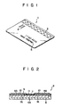
- Fig. 1 shows an electronic memory card according to an embodiment of the present invention.
- Electronic memory card 1 has a thickness of about 0.8 mm, and incorporates integrated circuit (IC) pellet 2, as will be described later.
- Magnetic stripe portion 3 and external connection terminal portion 4 are arranged on the front surface of card 1, and embossed portion 5 is formed on the back surface thereof.
- Magnetic data e.g., a verification code of the card
- Embossed portion 5 is formed by embossing to project from the back surface of card 1 or to be pitted in the front surface, so as to represent identification data (e.g., the name of a card holder, an identification code, and the like).
- identification data e.g., the name of a card holder, an identification code, and the like.
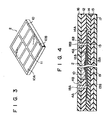
- a semiconductor element e.g., a MOS transistor serving as active region 6A is formed on silicon substrate 6, and insulating layer 7 (e.g., an Si0 2 layer), in which through holes 7A are formed at predetermined positions, is formed on active region 6A.
- insulating layer 7 e.g., an Si0 2 layer
- through holes 7A are formed at predetermined positions.
- Aluminum is formed on insulating layer 7 by a vapour deposition and is then etched to form an internal wiring pattern and electrode pads 8 to be connected to an external circuit.
- Insulating layer 9 e.g., an Si0 2 layer in which through holes 8A are formed at predetermined positions is formed on electrode pads 8.
- External electrode pads 10 are aligned on the uppermost surface of pellet 2 in a 4 x 2 matrix, and insulating layer 11 (e.g., an SiO 2 layer) is arranged between pads 10.
- insulating layer 11 e.g., an SiO 2 layer
- Some of electrode pads 10 in the 4 x 2 matrix are electrically connected to internal electrode pads 8 through corresponding through holes 8A, and the remaining electrode pads 10, e.g.; two lower electrode pads 10A and 10B, are auxiliary pads and are not connected to pads 8.
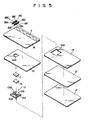
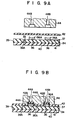
- intermediate inner core 14 for storing wiring substrate 13 is adhered to the lower surface of upper inner core 12 for storing IC pellet 2
- lower inner core 15 is adhered to the lower surface of core 14, as shown in Fig. 4.
- Upper- and lower-surface films 16 and 17 are laminated on the upper surface of core 12 and the lower surface of core 15, respectively.
- Films 16 and 17 are formed of a soft resin (e.g., poly-vinyl chloride added with plasticizer), and magnetic stripe portion 3 is formed on the surface of film 16.
- Inner cores 12, 14, and 15 are formed of a hard resin (e.g., vinyl chloride).
- Storage portion 12A for storing pellet 2 is formed in inner core 12, and storage portion 14A for storing wiring substrate 13 is formed in inner core 14 to correspond to portion 12A of core 12, as shown in Fig. 5.
- Wiring substrate 13 arranged in storage portion 14A of core 14 is a film-like sheet, and is slightly larger than pellet 2.
- Internal connection terminals 13A and external connection terminals 13B are aligned on the upper surface of substrate 13.
- Internal connection terminals 13A are connected to electrode pads 10 of pellet 2
- external connection terminals 13B are connected to contact terminals 18A, 18B, 18C,..., 18H of external connection terminal portion 4. More specifically, IC pellet 2 is adhered onto wiring substrate 13 through anisotropic conductive adhesive tape 19.
- internal connection terminals 13A are electrically connected to electrode pads 10 by tape 19.
- Tape 19 is prepared by mixing conductive particles 13C (e.g., Ni, Ai, Carbon, and the like) with hot-melt type insulating adhesive 30.
- conductive particles 13C e.g., Ni, Ai, Carbon, and the like
- Contact terminals 18A, 18C, 18D,..., ' 18H of terminal portion 4 connected to external connection terminals 13B of substrate 13 are formed of a conductive metal, and each has flat head portion 4A and projection 4B formed integrally therewith.
- thermo-compression bonding tool is brought into contact with head portions 4A of terminals 18A, 18B, 18C,..., 18H, and their projections 4B are inserted in upper inner core 12 from above film 16.
- projections 4B of terminals 18A, 18B, 18C,..., 18H heated by the bonding tool partially melt upper inner core 12, and are inserted therein until the lower ends of projections 4B are brought into contact with terminals 13B.
- Upper film 16 corresponding to head portions 4A of terminals 18A, 18B, 18C,..., 18H is locally gelled and, thereafter, is bonded to portions 4A after the bonding tool is released.
- terminals 18A, 18B, 18C,..., 18h are bonded to film 16 and inner core 12, and electrode pads 10 of IC pellet 2 are electrically connected to terminals 18A, 18B, 18C,..., 18H through wiring substrate 13.
- the upper surfaces of terminals 18A, 18B, 18C,..., 18H buried in film 16 are in substantially the same plane as that of the upper surface of film 16, and the upper surface of card 1 is flat.
- Terminals 18A and 18B of terminals 18A, 18B, 18C,..., 18H are auxiliary terminals, and are connected to pads 10A and 10B.
- Terminal 18C receives reference voltage Vcc
- terminal 18D serves as a GND terminal
- terminal 18E receives a reset signal
- terminal 18F receives a high voltage V pp for writing a data
- terminal 18G receives a clock signal
- terminal 18H receives address and data signals as input/output signals.
- each of contact terminals 18A, 18B, 18C,..., 18h of terminal portion 4 has a structure wherein each projection 4B extends from the lower surface of flat head portion 4A. Projections 4B are inserted in film 16 from above using a-thermo-compression bonding tool to partially gel film 16 and, thereafter, are bonded thereto. Therefore, contact terminals 18A, 18B, 18C,..., 18H can be effectively bonded to upper film 16 through a simple operation.
- FIG. 6 Another embodiment of the present invention will now be described with reference to Fig. 6.
- the same reference numerals in Fig. 6 denote the same portions as in Figs. 1 to 5, and a detailed description thereof will be omitted.
- wiring pattern 21 is arranged directly on the upper surface of inner core 20 for storing pellet 2, and pellet 2 and contact terminals 22 are connected to pattern 21.
- inner core 20 is made of a hard resin (e.g., vinyl chloride), and storage portion 20A is formed in a predetermined portion thereof.
- Wiring pattern 21 formed on inner core 20 is formed by etching a copper foil adhered to the entire surface of inner core 20 except for storage portion 20A.
- Connection leads 21A formed by extending wiring pattern 21 are connected to external connection pads 10 of IC pellet 2, and external connection terminals 21B are connected to contact terminals 22 of external connection terminal portion 4.
- each contact terminal 22 of terminal portion 4 has flat head portion 4A and projection 4B extending from the lower surface thereof, as in the first embodiment.
- Contact terminals 22 are compressed and inserted in upper film 16 from above by a thermo-compression bonding tool to partially gel a portion of film 16, and are then bonded thereto. Therefore, the lower ends of contact terminals 22 are connected to connection terminals 21B of wiring pattern 21.
- each contact terminal 22 is buried in film 16 so that its upper surface projects slightly from film 16, and is held in film 16 only by its bonding force. Note that upper and lower films 16 and 17 are laminated on the upper and lower surfaces of inner core 20.
- the above electronic memory card has a structure suited for mass-production, and has inner core 20 with a simple structure, thus reducing the thickness of the card.
- each contact terminal of external connection terminal portion 4 is thermally bonded directly to upper film 16 and upper inner core 12.
- each contact terminal can be bonded by simply compressing and inserting it therein.
- wiring substrate 34 is formed on a 300 ⁇ m thick flexible, rectangular plate formed of a hard vinyl chloride resin.
- Substantially square opening 34A for IC pellet 35 is formed in a region of wiring substrate 34, near the center of the card, as shown in Fig. 8.
- Eight contact portions 36 in a 2 x 4 matrix are formed to project in a region of wiring substrate 34, apart from the center of the card, as shown in Fig. 8.
- the projected portion of each contact portion 36 has substantially the same rectangular shape as that of an upper overcoat (to be described later), and has sharp edge portion 36A which projects from the upper outer periphery thereof.
- IC pellet 35 having the structure show in Fig. 2, thicker than wiring substrate 34, is fitted in opening 34A thereof, and electrodes 35A of pellet 35 are connected to contact portions 36 through conductor lead pattern 37 formed on wiring substrate 34.
- Lead pattern 37 is formed such that a copper foil is laminated on wiring substrate 34 and is then etched.
- Contact portions 36 are formed such that a copper foil is laminated on wiring substrate 34 and, after copper plating is performed on a portion of lead pattern 37 to a predetermined thickness, the resultant structure is etched to form sharp edge portion 36A on the upper surface.
- each contact portion 36 can be formed without copper plating such that the lower portion of a small copper segment, on which sharp edge portion 36A is formed by pressing, is fitted in and fixed to a hole formed in wiring substrate 34.
- the lower surface regions of connection portions 37A of lead pattern 37 to be connected to electrodes 35A are tin-plated.
- Gold bumps are formed on electrodes 35A, which corresponds to tin-plated connection portions 37A. Connection portions 37A of lead pattern 37 and electrodes 35A are connected so that gold and tin are welded by a pulse heating method.
- a seal resin is formed on IC pellet 35 by partial molding, thereby fixing IC pellet 35 to wiring substrate 34, and buries connection portions 37A of lead pattern 37 and electrodes 35A therewith.
- IC pellet 35 is arranged so that its lower portion projects from the lower surface of wiring substrate 34.
- Upper sheet 39 has a thickness of 300 ⁇ m and is formed of a hard resin (e.g., vinyl chloride). Upper sheet 39 has rectangular opening 39A, in which IC module 33 is fitted. Opening 39A is formed in sheet 39 to extend from one short side of the card, along magnetic stripe 32, as shown in Fig. 8.
- Lower sheet 40 has a thickness of 300 ⁇ m, is formed of a soft resin (e.g., poly-vinyl chloride added with plasticizer), and has opening 40A in which the lower portion of IC pellet 35 is fitted. Lower sheet 40 is adhered to IC-module 33 by an adhesive excluding these portions corresponding to the lower surface of upper sheet 39 and opening 34A of IC module 33.
- a soft resin e.g., poly-vinyl chloride added with plasticizer
- Upper and lower overcoats 42 and 43 have a thickness of 100 ⁇ m, respectively, and are formed of a hard resin (e.g., vinyl chloride). Upper and lower overcoats 42 and 43 respectively cover the upper surfaces of IC module 33 and upper sheet 39 and the lower surfaces of lower sheet 40 and IC pellet 35, and are adhered thereto by an adhesive. Eight small holes 42A in a 2 x 4 matrix are formed in upper overcoat 42 at positions corresponding to contact portions 36. Magnetic stripe 32 coated with iron oxide powder is formed on-upper overcoat 42 to extend along one long side of the card.
- a hard resin e.g., vinyl chloride
- Die 44 has recesses 44A suitable for the shape and arrangement of a plurality of contact portions 36, and recesses 44A communicate with air holes 44B. Each recess 44A has a depth slightly larger than the projecting length of each contact portion 36.
- Upper overcoat 42 is arranged above contact portions 36 projecting from wiring substrate 34, and die 44 is driven from above so that upper overcoat 42 is sandwiched between die 44 and contact portions 36, which serve as punches. Therefore, upper overcoat 42 is locally cut around the respective contact portions 36, and contact portions 36 are arranged in substantially the same plane as that of upper overcoat 42 to be externally exposed. When upper overcoat 42 is cut, the lower surface thereof is adhered to the upper surfaces of IC module 33 and upper sheet 39 by adhesive 31. Although cut segments 42B of upper overcoat 42 are left in recesses 44A of die 44, they are removed by airflow supplied from air holes 44B.
- upper overcoat 42 is punched by die 44 and contact portions 36 and, at the same time, upper overcoat 42 is adhered to upper sheet 39 and IC module 33 by adhesive 41.
- Lower overcoat 43 is then adhered to the lower surfaces of IC module 33 and lower sheet 40 by an adhesive.
- the outer periphery of the resultant structure is cut to a predetermined size, and magnetic stripe 32 is formed on upper overcoat 42, thus completing manufacture of an electronic memory card.
- openings 39A and 40A are respectively preformed in upper and lower sheets 39 and 40, and wiring substrate 34 and the lower portion of IC pellet 35 are respectively fitted therein, thus allowing easy alignment of IC module 33 and IC pellet 35. Therefore, electronic memory cards can be efficiently manufactured. Sharp edge portion 36A is formed on each contact portion 36, and small holes are formed in upper overcoat 42 using die 44 and contact portions 36, which serve as punches. During the formation of the small holes, upper overcoat 42 is adhered to upper sheet 39 and IC module 33. Therefore, the cost and the number of steps in the manufacture of the electronic memory card can be greatly reduced. In addition, since the electronic memory card has magnetic stripe 32, it can be used as a magnetic card.
Landscapes
- Engineering & Computer Science (AREA)
- Computer Hardware Design (AREA)
- Microelectronics & Electronic Packaging (AREA)
- Physics & Mathematics (AREA)
- General Physics & Mathematics (AREA)
- Theoretical Computer Science (AREA)
- Credit Cards Or The Like (AREA)
Applications Claiming Priority (2)
| Application Number | Priority Date | Filing Date | Title |
|---|---|---|---|
| JP151779/85 | 1985-07-10 | ||
| JP60151779A JPH0751390B2 (ja) | 1985-07-10 | 1985-07-10 | Icカ−ド |
Publications (3)
| Publication Number | Publication Date |
|---|---|
| EP0209791A2 true EP0209791A2 (fr) | 1987-01-28 |
| EP0209791A3 EP0209791A3 (en) | 1989-05-03 |
| EP0209791B1 EP0209791B1 (fr) | 1993-04-14 |
Family
ID=15526113
Family Applications (1)
| Application Number | Title | Priority Date | Filing Date |
|---|---|---|---|
| EP86109286A Expired - Lifetime EP0209791B1 (fr) | 1985-07-10 | 1986-07-08 | Carte à mémoire électronique |
Country Status (4)
| Country | Link |
|---|---|
| US (1) | US4795895A (fr) |
| EP (1) | EP0209791B1 (fr) |
| JP (1) | JPH0751390B2 (fr) |
| DE (1) | DE3688267T2 (fr) |
Cited By (7)
| Publication number | Priority date | Publication date | Assignee | Title |
|---|---|---|---|---|
| DE3912891A1 (de) * | 1989-04-19 | 1990-11-08 | Siemens Ag | Montagevorrichtung zur kontaktierung und zum einbau eines integrierten schaltkreissystems fuer eine wertkarte |
| FR2660092A1 (fr) * | 1990-03-26 | 1991-09-27 | Ryoden Kasei Kk | Procede de fabrication d'une carte a circuit integre. |
| EP0503782A1 (fr) * | 1991-03-15 | 1992-09-16 | Gec Avery Limited | Jeton avec circuit intégré |
| EP0688051A1 (fr) * | 1994-06-15 | 1995-12-20 | Philips Cartes Et Systemes | Procédé de fabrication et d'assemblage de carte à circuit intégré et carte ainsi obtenue |
| FR2740644A1 (fr) * | 1995-10-26 | 1997-04-30 | Gemplus Sca | Procede de fabrication d'un transducteur sonore integre dans une carte a production de signaux acoustiques |
| EP0676717A3 (fr) * | 1994-04-11 | 1997-06-04 | At & T Corp | Support flexible, fin et résistant pour cartes à circuit intégré. |
| DE4345473B4 (de) * | 1993-11-06 | 2006-03-23 | Ods Landis & Gyr Gmbh & Co. Kg | Kontaktlose Chipkarte mit Antennenspule |
Families Citing this family (32)
| Publication number | Priority date | Publication date | Assignee | Title |
|---|---|---|---|---|
| FR2617666B1 (fr) * | 1987-07-02 | 1989-10-27 | Bull Cp8 | Carte a microcircuits electroniques et son procede de fabrication |
| US5304513A (en) * | 1987-07-16 | 1994-04-19 | Gao Gesellschaft Fur Automation Und Organisation Mbh | Method for manufacturing an encapsulated semiconductor package using an adhesive barrier frame |
| US4931991A (en) * | 1988-12-22 | 1990-06-05 | Amp Incorporated | Machine readable memory card with capacitive interconnect |
| JPH0291360U (fr) * | 1988-12-29 | 1990-07-19 | ||
| US5016919A (en) * | 1989-03-10 | 1991-05-21 | Frank Rotondo | Check and magnetic strip arrangement |
| JPH0687484B2 (ja) * | 1989-04-06 | 1994-11-02 | 三菱電機株式会社 | Icカード用モジュール |
| US5093985A (en) * | 1989-06-30 | 1992-03-10 | John Houldsworth | Method of assembly for small electrical devices |
| FR2667713A1 (fr) * | 1990-10-08 | 1992-04-10 | Cit Alcatel | Lecteur de carte a micro-circuit, a encombrement reduit. |
| CA2051836C (fr) * | 1990-11-30 | 1996-07-23 | Richard Michael Flynn | Fabrication d'une carte de donnees personnelle |
| KR950012290B1 (ko) * | 1993-05-14 | 1995-10-16 | 삼성전자주식회사 | 메모리 모듈 |
| US5817207A (en) | 1995-10-17 | 1998-10-06 | Leighton; Keith R. | Radio frequency identification card and hot lamination process for the manufacture of radio frequency identification cards |
| US5708419A (en) * | 1996-07-22 | 1998-01-13 | Checkpoint Systems, Inc. | Method of wire bonding an integrated circuit to an ultraflexible substrate |
| DE10239564A1 (de) * | 2002-08-28 | 2005-03-17 | Giesecke & Devrient Gmbh | Tragbarer Datenträger mit Anzeigevorrichtung |
| NL1022766C2 (nl) * | 2003-02-24 | 2004-09-21 | Enschede Sdu Bv | Identiteitskaart alsmede reisdocument. |
| USD517602S1 (en) * | 2004-09-10 | 2006-03-21 | Retail Royalty Company | Credit card |
| EP2461275A1 (fr) * | 2010-12-02 | 2012-06-06 | Gemalto SA | Document de sécurité et son procédé de fabrication |
| USD729808S1 (en) * | 2013-03-13 | 2015-05-19 | Nagrastar Llc | Smart card interface |
| USD759022S1 (en) * | 2013-03-13 | 2016-06-14 | Nagrastar Llc | Smart card interface |
| US9647997B2 (en) | 2013-03-13 | 2017-05-09 | Nagrastar, Llc | USB interface for performing transport I/O |
| US9888283B2 (en) | 2013-03-13 | 2018-02-06 | Nagrastar Llc | Systems and methods for performing transport I/O |
| USD758372S1 (en) * | 2013-03-13 | 2016-06-07 | Nagrastar Llc | Smart card interface |
| USD780763S1 (en) * | 2015-03-20 | 2017-03-07 | Nagrastar Llc | Smart card interface |
| USD864968S1 (en) | 2015-04-30 | 2019-10-29 | Echostar Technologies L.L.C. | Smart card interface |
| JP1647393S (fr) | 2018-02-01 | 2019-12-09 | ||
| USD930000S1 (en) | 2018-10-12 | 2021-09-07 | Huawei Technologies Co., Ltd. | Memory card |
| US10817768B1 (en) | 2019-12-20 | 2020-10-27 | Capital One Services, Llc | Systems and methods for preventing chip fraud by inserts in chip pocket |
| US11049822B1 (en) | 2019-12-20 | 2021-06-29 | Capital One Services, Llc | Systems and methods for the use of fraud prevention fluid to prevent chip fraud |
| US10888940B1 (en) | 2019-12-20 | 2021-01-12 | Capital One Services, Llc | Systems and methods for saw tooth milling to prevent chip fraud |
| US10810475B1 (en) | 2019-12-20 | 2020-10-20 | Capital One Services, Llc | Systems and methods for overmolding a card to prevent chip fraud |
| USD983261S1 (en) | 2019-12-20 | 2023-04-11 | Capital One Services, Llc | Vented laminated card |
| US10977539B1 (en) | 2019-12-20 | 2021-04-13 | Capital One Services, Llc | Systems and methods for use of capacitive member to prevent chip fraud |
| US11715103B2 (en) | 2020-08-12 | 2023-08-01 | Capital One Services, Llc | Systems and methods for chip-based identity verification and transaction authentication |
Family Cites Families (14)
| Publication number | Priority date | Publication date | Assignee | Title |
|---|---|---|---|---|
| US3702464A (en) * | 1971-05-04 | 1972-11-07 | Ibm | Information card |
| FR2205800B1 (fr) * | 1972-11-09 | 1976-08-20 | Honeywell Bull Soc Ind | |
| US4222516A (en) * | 1975-12-31 | 1980-09-16 | Compagnie Internationale Pour L'informatique Cii-Honeywell Bull | Standardized information card |
| DE2920012C2 (de) * | 1979-05-17 | 1988-09-29 | GAO Gesellschaft für Automation und Organisation mbH, 8000 München | Ausweiskarte mit IC-Baustein und Verfahren zur Herstellung einer derartigen Ausweiskarte |
| FR2486685B1 (fr) * | 1980-07-09 | 1985-10-31 | Labo Electronique Physique | Carte de paiement electronique et procede de realisation |
| DE3130206A1 (de) * | 1981-07-30 | 1983-02-17 | Siemens AG, 1000 Berlin und 8000 München | Tragbare karte zur informationsverarbeitung |
| DE3151408C1 (de) * | 1981-12-24 | 1983-06-01 | GAO Gesellschaft für Automation und Organisation mbH, 8000 München | Ausweiskarte mit einem IC-Baustein |
| FR2527036A1 (fr) * | 1982-05-14 | 1983-11-18 | Radiotechnique Compelec | Procede pour connecter un semiconducteur a des elements d'un support, notamment d'une carte portative |
| CA1204213A (fr) * | 1982-09-09 | 1986-05-06 | Masahiro Takeda | Carte a memoire protegee contre l'electricite statique |
| JPS59229686A (ja) * | 1983-06-09 | 1984-12-24 | Toshiba Corp | Icカ−ド |
| DE3338597A1 (de) * | 1983-10-24 | 1985-05-02 | GAO Gesellschaft für Automation und Organisation mbH, 8000 München | Datentraeger mit integriertem schaltkreis und verfahren zur herstellung desselben |
| US4727246A (en) * | 1984-08-31 | 1988-02-23 | Casio Computer Co., Ltd. | IC card |
| JPS61123990A (ja) * | 1984-11-05 | 1986-06-11 | Casio Comput Co Ltd | Icカ−ド |
| DE3533791A1 (de) * | 1985-09-21 | 1987-03-26 | Basf Ag | Chinoxalinderivate, ein verfahren zu ihrer herstellung und ihre verwendung zum schutz von kulturpflanzen vor der phytotoxischen wirkung von herbiziden |
-
1985
- 1985-07-10 JP JP60151779A patent/JPH0751390B2/ja not_active Expired - Fee Related
-
1986
- 1986-07-02 US US06/881,221 patent/US4795895A/en not_active Expired - Lifetime
- 1986-07-08 EP EP86109286A patent/EP0209791B1/fr not_active Expired - Lifetime
- 1986-07-08 DE DE86109286T patent/DE3688267T2/de not_active Expired - Fee Related
Cited By (10)
| Publication number | Priority date | Publication date | Assignee | Title |
|---|---|---|---|---|
| DE3912891A1 (de) * | 1989-04-19 | 1990-11-08 | Siemens Ag | Montagevorrichtung zur kontaktierung und zum einbau eines integrierten schaltkreissystems fuer eine wertkarte |
| FR2660092A1 (fr) * | 1990-03-26 | 1991-09-27 | Ryoden Kasei Kk | Procede de fabrication d'une carte a circuit integre. |
| US5346576A (en) * | 1990-03-26 | 1994-09-13 | Mitsubishi Denki Kabushiki Kaisha | Method of manufacturing IC card |
| EP0503782A1 (fr) * | 1991-03-15 | 1992-09-16 | Gec Avery Limited | Jeton avec circuit intégré |
| DE4345473B4 (de) * | 1993-11-06 | 2006-03-23 | Ods Landis & Gyr Gmbh & Co. Kg | Kontaktlose Chipkarte mit Antennenspule |
| EP0676717A3 (fr) * | 1994-04-11 | 1997-06-04 | At & T Corp | Support flexible, fin et résistant pour cartes à circuit intégré. |
| EP0688051A1 (fr) * | 1994-06-15 | 1995-12-20 | Philips Cartes Et Systemes | Procédé de fabrication et d'assemblage de carte à circuit intégré et carte ainsi obtenue |
| FR2740644A1 (fr) * | 1995-10-26 | 1997-04-30 | Gemplus Sca | Procede de fabrication d'un transducteur sonore integre dans une carte a production de signaux acoustiques |
| WO1997016049A1 (fr) * | 1995-10-26 | 1997-05-01 | Gemplus | Procede de fabrication d'un transducteur sonore integre dans une carte a production de signaux acoustiques |
| US6272228B1 (en) | 1995-10-26 | 2001-08-07 | Gemplus | Method for making a sound transducer integrated into an acoustic signal generating card |
Also Published As
| Publication number | Publication date |
|---|---|
| US4795895A (en) | 1989-01-03 |
| EP0209791B1 (fr) | 1993-04-14 |
| DE3688267D1 (de) | 1993-05-19 |
| JPH0751390B2 (ja) | 1995-06-05 |
| JPS6211696A (ja) | 1987-01-20 |
| EP0209791A3 (en) | 1989-05-03 |
| DE3688267T2 (de) | 1993-11-04 |
Similar Documents
| Publication | Publication Date | Title |
|---|---|---|
| US4795895A (en) | Multi-layered electronic card carrying integrated circuit pellet and having two-pad layered structure for electrical connection thereto | |
| US4889980A (en) | Electronic memory card and method of manufacturing same | |
| JP2849594B2 (ja) | 電子モジュールの封止方法 | |
| US4719140A (en) | Electronic memory card | |
| US4539472A (en) | Data processing card system and method of forming same | |
| US4835846A (en) | Method of manufacture of electronic modules for cards with microcircuits | |
| US4999742A (en) | Electronic module for a small portable object such as a card or a key incorporating an integrated circuit | |
| US5255430A (en) | Method of assembling a module for a smart card | |
| WO1989001873A1 (fr) | Dispositif a circuit integre et procede de fabrication dudit circuit | |
| HK84095A (en) | Method for mounting an integrated circuit on a support, resultant device and its use in an electronic microcircuit card | |
| JP2953899B2 (ja) | 半導体装置 | |
| US4907061A (en) | Electronic device | |
| JPH054914B2 (fr) | ||
| JPH0216233B2 (fr) | ||
| JP4306352B2 (ja) | 接触型非接触型ハイブリットicモジュールとそれを使用した接触型非接触型ハイブリットicカード | |
| JPS61139894A (ja) | Idカ−ドおよびその製造方法 | |
| JP3769332B2 (ja) | Icカードの製造方法 | |
| EP0212020B1 (fr) | Système de traitement de données sous forme de carte et son procédé de fabrication | |
| JPH0262297A (ja) | 集積回路装置およびそれを用いたicカード | |
| CA1242528A (fr) | Systeme de cartes de traitement de donnees et methode de construction de ce systeme | |
| JPH05509267A (ja) | 携帯可能なデータ媒体装置の製造方法 | |
| JPS6283196A (ja) | Icカ−ド | |
| JPH02134859A (ja) | マルチチップ半導体装置とその製造方法 | |
| JPS6211695A (ja) | Icカードの製造方法 | |
| JPH0276798A (ja) | 集積回路装置の製造方法 |
Legal Events
| Date | Code | Title | Description |
|---|---|---|---|
| PUAI | Public reference made under article 153(3) epc to a published international application that has entered the european phase |
Free format text: ORIGINAL CODE: 0009012 |
|
| AK | Designated contracting states |
Kind code of ref document: A2 Designated state(s): DE FR NL SE |
|
| PUAL | Search report despatched |
Free format text: ORIGINAL CODE: 0009013 |
|
| AK | Designated contracting states |
Kind code of ref document: A3 Designated state(s): DE FR NL SE |
|
| 17P | Request for examination filed |
Effective date: 19890906 |
|
| 17Q | First examination report despatched |
Effective date: 19910208 |
|
| GRAA | (expected) grant |
Free format text: ORIGINAL CODE: 0009210 |
|
| AK | Designated contracting states |
Kind code of ref document: B1 Designated state(s): DE FR NL SE |
|
| REF | Corresponds to: |
Ref document number: 3688267 Country of ref document: DE Date of ref document: 19930519 |
|
| ET | Fr: translation filed | ||
| PLBE | No opposition filed within time limit |
Free format text: ORIGINAL CODE: 0009261 |
|
| STAA | Information on the status of an ep patent application or granted ep patent |
Free format text: STATUS: NO OPPOSITION FILED WITHIN TIME LIMIT |
|
| 26N | No opposition filed | ||
| EAL | Se: european patent in force in sweden |
Ref document number: 86109286.4 |
|
| PGFP | Annual fee paid to national office [announced via postgrant information from national office to epo] |
Ref country code: FR Payment date: 19960709 Year of fee payment: 11 |
|
| PGFP | Annual fee paid to national office [announced via postgrant information from national office to epo] |
Ref country code: DE Payment date: 19960712 Year of fee payment: 11 |
|
| PGFP | Annual fee paid to national office [announced via postgrant information from national office to epo] |
Ref country code: SE Payment date: 19960717 Year of fee payment: 11 |
|
| PGFP | Annual fee paid to national office [announced via postgrant information from national office to epo] |
Ref country code: NL Payment date: 19960729 Year of fee payment: 11 |
|
| PG25 | Lapsed in a contracting state [announced via postgrant information from national office to epo] |
Ref country code: SE Effective date: 19970709 |
|
| PG25 | Lapsed in a contracting state [announced via postgrant information from national office to epo] |
Ref country code: NL Free format text: LAPSE BECAUSE OF NON-PAYMENT OF DUE FEES Effective date: 19980201 |
|
| PG25 | Lapsed in a contracting state [announced via postgrant information from national office to epo] |
Ref country code: FR Free format text: LAPSE BECAUSE OF NON-PAYMENT OF DUE FEES Effective date: 19980331 |
|
| NLV4 | Nl: lapsed or anulled due to non-payment of the annual fee |
Effective date: 19980201 |
|
| PG25 | Lapsed in a contracting state [announced via postgrant information from national office to epo] |
Ref country code: DE Free format text: LAPSE BECAUSE OF NON-PAYMENT OF DUE FEES Effective date: 19980401 |
|
| EUG | Se: european patent has lapsed |
Ref document number: 86109286.4 |
|
| REG | Reference to a national code |
Ref country code: FR Ref legal event code: ST |