EP0211634A2 - Verfahren und Gerät zur Herstellung von Halbleitervorrichtungen - Google Patents
Verfahren und Gerät zur Herstellung von Halbleitervorrichtungen Download PDFInfo
- Publication number
- EP0211634A2 EP0211634A2 EP86305952A EP86305952A EP0211634A2 EP 0211634 A2 EP0211634 A2 EP 0211634A2 EP 86305952 A EP86305952 A EP 86305952A EP 86305952 A EP86305952 A EP 86305952A EP 0211634 A2 EP0211634 A2 EP 0211634A2
- Authority
- EP
- European Patent Office
- Prior art keywords
- semiconductor
- semiconductor layer
- substrate
- dangling bonds
- semiconductor material
- Prior art date
- Legal status (The legal status is an assumption and is not a legal conclusion. Google has not performed a legal analysis and makes no representation as to the accuracy of the status listed.)
- Granted
Links
Images


Classifications
-
- H—ELECTRICITY
- H10—SEMICONDUCTOR DEVICES; ELECTRIC SOLID-STATE DEVICES NOT OTHERWISE PROVIDED FOR
- H10F—INORGANIC SEMICONDUCTOR DEVICES SENSITIVE TO INFRARED RADIATION, LIGHT, ELECTROMAGNETIC RADIATION OF SHORTER WAVELENGTH OR CORPUSCULAR RADIATION
- H10F71/00—Manufacture or treatment of devices covered by this subclass
- H10F71/10—Manufacture or treatment of devices covered by this subclass the devices comprising amorphous semiconductor material
-
- H—ELECTRICITY
- H10—SEMICONDUCTOR DEVICES; ELECTRIC SOLID-STATE DEVICES NOT OTHERWISE PROVIDED FOR
- H10P—GENERIC PROCESSES OR APPARATUS FOR THE MANUFACTURE OR TREATMENT OF DEVICES COVERED BY CLASS H10
- H10P95/00—Generic processes or apparatus for manufacture or treatments not covered by the other groups of this subclass
- H10P95/94—Hydrogenation or deuterisation, e.g. using atomic hydrogen from a plasma
-
- Y—GENERAL TAGGING OF NEW TECHNOLOGICAL DEVELOPMENTS; GENERAL TAGGING OF CROSS-SECTIONAL TECHNOLOGIES SPANNING OVER SEVERAL SECTIONS OF THE IPC; TECHNICAL SUBJECTS COVERED BY FORMER USPC CROSS-REFERENCE ART COLLECTIONS [XRACs] AND DIGESTS
- Y02—TECHNOLOGIES OR APPLICATIONS FOR MITIGATION OR ADAPTATION AGAINST CLIMATE CHANGE
- Y02E—REDUCTION OF GREENHOUSE GAS [GHG] EMISSIONS, RELATED TO ENERGY GENERATION, TRANSMISSION OR DISTRIBUTION
- Y02E10/00—Energy generation through renewable energy sources
- Y02E10/50—Photovoltaic [PV] energy
-
- Y—GENERAL TAGGING OF NEW TECHNOLOGICAL DEVELOPMENTS; GENERAL TAGGING OF CROSS-SECTIONAL TECHNOLOGIES SPANNING OVER SEVERAL SECTIONS OF THE IPC; TECHNICAL SUBJECTS COVERED BY FORMER USPC CROSS-REFERENCE ART COLLECTIONS [XRACs] AND DIGESTS
- Y02—TECHNOLOGIES OR APPLICATIONS FOR MITIGATION OR ADAPTATION AGAINST CLIMATE CHANGE
- Y02P—CLIMATE CHANGE MITIGATION TECHNOLOGIES IN THE PRODUCTION OR PROCESSING OF GOODS
- Y02P70/00—Climate change mitigation technologies in the production process for final industrial or consumer products
- Y02P70/50—Manufacturing or production processes characterised by the final manufactured product
-
- Y—GENERAL TAGGING OF NEW TECHNOLOGICAL DEVELOPMENTS; GENERAL TAGGING OF CROSS-SECTIONAL TECHNOLOGIES SPANNING OVER SEVERAL SECTIONS OF THE IPC; TECHNICAL SUBJECTS COVERED BY FORMER USPC CROSS-REFERENCE ART COLLECTIONS [XRACs] AND DIGESTS
- Y10—TECHNICAL SUBJECTS COVERED BY FORMER USPC
- Y10S—TECHNICAL SUBJECTS COVERED BY FORMER USPC CROSS-REFERENCE ART COLLECTIONS [XRACs] AND DIGESTS
- Y10S148/00—Metal treatment
- Y10S148/004—Annealing, incoherent light
-
- Y—GENERAL TAGGING OF NEW TECHNOLOGICAL DEVELOPMENTS; GENERAL TAGGING OF CROSS-SECTIONAL TECHNOLOGIES SPANNING OVER SEVERAL SECTIONS OF THE IPC; TECHNICAL SUBJECTS COVERED BY FORMER USPC CROSS-REFERENCE ART COLLECTIONS [XRACs] AND DIGESTS
- Y10—TECHNICAL SUBJECTS COVERED BY FORMER USPC
- Y10S—TECHNICAL SUBJECTS COVERED BY FORMER USPC CROSS-REFERENCE ART COLLECTIONS [XRACs] AND DIGESTS
- Y10S148/00—Metal treatment
- Y10S148/024—Defect control-gettering and annealing
Definitions
- This invention relates to an improved method and apparatus for manufacturing semiconductor devices which has particular application to photoelectric conversion devices.
- Processing techniques are known for the fabrication of semiconductor devices comprising a substrate and a non-monocrystalline semiconductor layer formed on the substrate.
- some undesirable effects have been observed.
- a highly purified semiconductor exhibits a decrease in electric conductivity under photo annealing in atmospheric air and that its conductivity can recover under thermal annealing. The effect appears repeatedly.
- this phenomenon known as the Staebler-Wronski effect, is observed only on semiconductors taken out of a vacuum chamber and brought into contact with the atmosphere.
- Staebler-Wronski effect causes a cyclical change in the electrical conductivity of a semiconductor device, but also the conductivity tends to gradually decrease with repetition of the Staebler-Wronski effect. This is clearly undesirable, especially in semiconductors to be applied to solar cells, and like photoelectric conversion devices.
- An object of the present invention is thus to produce improved semiconductors which are thermally and optically more stable than the semiconductors produced hitherto.
- the present invention resides in the appreciation that the disadvantageous Staebler-Wronski effect arises on account of the presence of recombination instabilities in the surface microstructure of the semiconductor and that these instabilities can be largely eradicated if the semiconductor is fabricated in a manner which encourages the development of dangling bonds on its surface and if stable bondings are then made to the dangling bonds.
- the thus formed layer is irradiated within an evacuated chamber before it is exposed to atmospheric air so as to encourage the formation of dangling bonds and a gaseous neutralizing agent is then admitted to the chamber so as to stabilize the dangling bonds.
- the resulting semiconductor exhibits substantially increased stability as compared to conventionally fabricated semiconductors exhibiting the Staebler-Wronski effect.
- the neutralizing agent employed to stabilize the dangling bonds can be any one or more of fluorine, chlorine, oxygen, nitrogen, argon, krypton, xenon, helium or hydrogen gas, or can be a fluoride, a chloride or an oxide in combination with UV light irradiation to break down the compound into its atomic constituents.
- the requirement is that the neutralizing agent should be capable of binding to the dangling bonds in stable fashion.
- the invention extends not only to a manufacturing process for fabrication of improved semiconductors and to semiconductors fabricated in accordance with such process, but also to an improved fabrication apparatus hereinafter described for carrying out the process according to the invention.
- a substrate 10' made of artificial quartz is placed below a heater 12' in a first pre-stage chamber 1.
- the substrate 10' is provided with a pair of electrodes (designated as 24 and 24' in Fig. 2) for measuring electric conductivity.
- These electrodes can be contacted with a pair of probes 17 and 17' from outside of the chamber 1 after formation of a semiconductor layer on the substrate so that it is possible to measure the conductivity of the semiconductor in situ in the presence of light and in the absence of light, without the semiconductor making contact with atmospheric air.
- the substrate 10' can be transported with the heater 12' between the first chamber 1 and a second pre-stage chamber 2 through the gate valve 3.
- the second pre-stage chamber 2 is connected to a criosorption pump 6 through a second gate valve 5 and to a turbo molecular pump 8 through a third gate valve 7.
- the turbo molecular pump 8 is driven to evacuate the interiors of the first and second chambers 1 and 2 with the gate valves 3 and 7 opened and the gate valves 5 and 4 closed.
- a pressure of 10-6 torr or less has been attained in the chambers 1 and 2
- the heater 12' with the substrate 10' are transported from the first chamber 1 to the second chamber 2 by means of a first transportation mechanism 19.
- the interior of the second chamber 2 is further evacuated to a pressure of the order of 10 -10 torr with the gate valves 3 and 7 closed and the gate valve 5 opened by means of the criosorption pump 6.
- the interior of a reaction chamber 11 can be evacuated to a negative pressure of the order of 10 -9 to 10 - 10 torr by means of a second criosorption pump 9 which is connected to the reaction chamber 11 through a gate valve 22, and when it has been thus evacuated the substrate 10 on the heater 12 is transported from the second pre-stage chamber 2 and through the open gate valve 4 and into the reaction chamber 11 by means of a second transportation mechanism 19'.
- the valve 4 is closed and a plasma discharge is established between a pair of electrodes 14 and 15 which are supplied with power from-a high frequency voltage supply 13 so as to carry out a plasma CVD method of semiconductor deposition on the substrate 10.
- light irradiation may be carried out by irradiating the interior of the reaction chamber 11 with an eximer laser or the like through a window 16.
- the reactive gas for the plasma CVD method of semiconductor deposition is introduced into reaction chamber 11 from a doping system 21.
- the pressure of the reaction chamber is kept to the optimum level most suitable for carrying out the CVD semiconductor deposition method by means of the turbo molecular pump 9.
- the pressure in the reaction chamber 11 is generally kept between 0.001 and 0.1 torr, and is normally between 0.05 and 0.1 torr.
- a non-monocrystalline semiconductor film an amorphous silicon doped with hydrogen in this embodiment, is formed in accordance with the plasma CVD method.
- a non-monocrystalline semiconductor layer of thickness 0.6 ⁇ which may or may not be doped with p-type or n-type impurities may be formed on the substrate 10 at a temperature of 250°C or less than 500°C.
- the reactive gas required for the CVD process and a carrier gas should be purified to the level at which their inclusion rates of oxygen and water are reduced to the order of less than 0.1 ppm, and more preferably to less than 1 ppb, before their introduction to the reaction chamber 11. This is in order to reduce the density of oxygen within the semiconductor to less than 5 x 10 18 cm -3 , and more preferably less than 1 x 10 18 cm -3 .
- the reactive gas can for example be silane which has been highly purified as by liquefaction purification as for the fabrication of silicon film.
- the silane gas may be dosed with diborane at 500 to 5000 ppm.
- the silane gas may be dosed with phosphine at about 5000 ppm.
- the impurit.ies are introduced via an inlet port 21".
- the substrate 10 on the heater 12 is transported from the reaction chamber 11 to the first pre-stage chamber 1 via the second pre-stage chamber 2 with the gate valves 3 and 4 opened. Then, with the gate valve 4 closed and the gate valve 5 opened, the pressure in the first pre-stage chamber 1 is kept at a prescribed negative pressure by means of the criosorption pump 6.
- This negative pressure may be less than 10 -3 torr, and preferably is between 10 6 and 10 -9 torr.
- the semiconductor 10 is maintained at a temperature of less than 50°C so that it does not experience thermal annealing, and is irradiated with light without being allowed to make contact with the atmospheric air.
- dangling bonds are caused to appear on the semiconductor and these are thereafter neutralized by the introduction into the chamber 1 via the dosing system 25 of a neutralizing agent such as fluorine, chlorine, oxygen, nitrogen, argon, krypton, xenon, helium or hydrogen.
- a neutralizing agent such as fluorine, chlorine, oxygen, nitrogen, argon, krypton, xenon, helium or hydrogen.
- fluorine gas of a purity of 99% or higher is suitable. This can be obtained by liquefaction purification, namely, fluorine (m.p.-223°C, v.p.-187°c) retained in a vessel is liquefied by means of liquefied nitrogen. Then, the liquefied fluorine is vaporized under negative pressure and is recovered as very highly purified fluorine. By virtue of this processing, the fluorine is estimated to have higher than 99.99% purity with very little included oxygen and a dew point lower than -60°C.
- the fluorine permeates into the microstructure of the semiconductor surface and neutralizes the dangling bonds which were caused to appear on the semiconductor surface by the photo annealing.
- the fluorine also substitutes Si-F bondings for Si-H bondings which have relatively weak bonding forces.
- Fig. 2 shows the semiconductor layer 26 on the substrate 10 fabricated as described above.
- the substrate 10 is made of a synthetic quartz.
- the semiconductor layer 26 is made of a non-monocrystal amorphous silicon doped with hydrogen or halogen.
- the semiconductor layer 10 was subjected to repeated light irradiation annealing and thermal annealing for examining the change in conductivity of the semiconductor layer 10.
- the photo annealing was carried out using a halogen lamp (100mW/cm 2 ) and the thermal annealing was carried out by supplying power to the heater 12.
- the conductivity was measured by means of the pair of probes 17 and 17' in contact with the pair of electrodes 24 and 24' and with the semiconductor at a negative pressure.
- Fig. 3 shows how the conductivity of a conventionally manufactured semiconductor varies under alternate thermal annealing and photo annealing under atmospheric conditions.
- the conventional semiconductor under consideration comprised a silicon semiconductor layer of 0.6 ⁇ thickness formed on a quartz glass plate.
- the conductivity of the semiconductor in the presence of light is referred to as its photo conductivity and the conductivity in the absence of light is referred to as its dark conductivity.
- the initial photo conductivity is designated as 28-1, and the initial dark conductivity as 28'-1.
- the semiconductor layer was then irradiated with light of AM1(100mW/cm ) from a xenon lamp for a determined period and the resulting photo and dark conductivities 28-2 and 28'-2' showed a decrease from their initial levels.
- thermal annealing was carried out at 150°C for 2 hours, and the resulting conductivities 28-3 and 28'-3 showed an increase from their preceding levels. In this manner, thermal and photo annealing steps were repeated one after another.
- the Staebler-Wronski effect was demonstrated as shown in Fig. 3, with both the photo and dark conductivities being repetitively decreased by photo annealing and subsequently increased by thermal annealing.
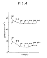
- Figs. 4 through 8 the variation of the conductivity of a semiconductor layer manufactured in accordance with the present invention is shown with the semiconductor repetitively subjected to optical and thermal annealings carried out alternately as described above.
- the measurement results are designated by 29-1, 29-2,...29-7 and by 29'-1, 29'-2,...29'-7 with the references 1,2,...7 indicating the ordinal number of the corresponding measurement and with the references preceded by 29 indicating a photo conductivity measurement and the references preceded by 29' indicating a dark conductivity measurement, and a similar system of reference numerals is used in the other figures.
- Fig. 4 is a graphical showing of the conductivity variations of a semiconductor layer formed in accordance with the present invention but without treatment with the neutralizing agent, the conductivity measurements having been made in the pre-stage chamber 1 under negative pressure and without exposing the semiconductor to contact with air.
- a dark conductivity 29'-1 of 1.5 x 10 -8 Scm -1 and a photo conductivity 29-1 of 9 x 10 -5 Scm -1 was obtained at 25°C and 4 x 10 -8 torr.
- the semiconductor layer was subjected to photo annealing for two hours at 100mW/cm by irradiation with a xenon lamp.
- a dark conductivity 29'-2 of 6 x 10 - 9 Scm -1 and a photo conductivity 29-2 of 3.5 x 10 -5 Sem -1 were obtained indicating decreases from the initial levels as in the prior art.
- the semiconductor was subjected to thermal annealing for 3 hours at 150°C. Unexpectedly, as a result, the conductivity further decreased unlike the conventional situation.
- This phenomenon which we have discovered has been named by us as the SEL effect, this terminology being derived from the words "State Exited by Light”. The reason why this SEL effect takes place, instead of the Staebler-Wronski effect, is believed to be because dangling bonds formed on the semiconductor remain intact during repeated photo and thermal annealing in the evacuated chamber.
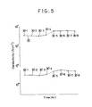
- Fig. 5 shows the conductivity of a semiconductor layer measured in situ in the device of Fig. 1 with oxygen introduced at 4'x 10 4 Pa, that is approximately the same pressure as the partial pressure of oxygen in atmospheric air, into the first pre-stage chamber as a neutralizing agent.
- the values 30-1 and 30'-1 designate the photo and dark conductivities respectively before the introduction of oxygen
- the values 30-2 and 30'-2 designate the photo and dark conductivities respectively after the introduction of oxygen.
- the semiconductor was irradiated with light from a halogen lamp at 100 W/cm 2 for two hours. As a result the measured conductivities 30-3 and 30'-3 were found to remain substantially as they were, although a slight decrease was observed.
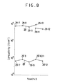
- Fig. 6 shows another example of the conductivity variations of a semiconductor fabricated by the method of the invention with dangling bonds neutralized by a neutralizer agent.
- the semiconductor was irradiated with light for 48 hours, or at least more than 3 hours so that a sufficient number of dangling bonds appeared, and highly purified fluorine gas was introduced into the pre-stage chamber in order to neutralize the dangling bonds according to the formula
- the Si-F binding is expected to be stable even in atmospheric air.
- the electronegativity of fluorine is 4.0 while the electronegativity of oxide is 3.5.
- Photo and thermal annealings were repeatedly carried out under the same condition as described above with reference to Fig. 3. As may be seen from Fig. 6, the conductivity did not fluctuate substantially. From this experiment it may be deduced that few recombination centers reappear on the semiconductor.
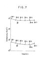
- Fig. 7 the conductivity variations of a further embodiment are shown.
- measured results 29-1 to 29-5, and 29'-1 to 29'-5 are obtained under the same conditions and using the same kind of specimen as described with reference to Fig. 4.
- argon gas was introduced into the pre-stage chamber where it connected to the dangling bonds residing on the microstructure of the semiconductor surface.
- the SEL effect was observed at atmospheric pressure and at low pressure (10-2 to 10 - 6 torr).
- the semiconductor was treated by thermal annealing at 100 to 500°C in an atmosphere of argon excited by ultraviolet light.
- the conductivity of the semiconductor thus treated is shown by 29-6 and 29'-6.
- Krypton, xenon, helium, hydrogen and mixtures of two or more thereof can effectively be used instead of argon and, in addition, the existence of a trace quantity of natrium is very advantageous for stabilizing the conductivity characteristics of the semiconductor.
- the recombination center density in a semiconductor manufactured according to the present invention is estimated to be less than about 1 x 10 17 to 1 x 10 18 cm -3 , and in some cases less than 5 x 10 16 cm -3 .
- the neutralization process can be carried out in another chamber separate from the manufacturing device of Fig. 1.
- the semiconductor After irradiation, the semiconductor can be thermally processed at 100 to 500°C, and more desirably 250 to 300°C, at ambient pressure in an atmosphere of a fluorine mixture made active by ultraviolet light irradiation.
- a fluorine mixture made active by ultraviolet light irradiation.
- the present invention is also applicable to the fabrication of semiconductor layers by a photo CVD method.
- Si x C 1-x (0 ⁇ X ⁇ 1), Si x Sn 1-X (0 ⁇ X ⁇ 1) Si x Ge 1-X (0 ⁇ X ⁇ .1), in which hydrogen and/or fluorine is doped, or amorphous silicon fluoride or other non-monocrystalline semiconductors can be applied to the practice of the invention.
- fluorides such as HF, CFH 3 , CH 2 F 2 , CF 4 , GeF 4 , Si 2 F 6 and so on, and chlorides such as HC1, CHC1 3 , CH 2 Cl 2 , CCl 2 F 2 and so on can be employed with ultraviolet light irradiation.
- chlorides such as HC1, CHC1 3 , CH 2 Cl 2 , CCl 2 F 2 and so on can be employed with ultraviolet light irradiation.
- oxides can be used in co-operation with ultraviolet light which decomposes the oxide into atoms.
- additives utilized in the practice of the invention as neutralizers are utilized in an entirely different manner from the way they are used in the prior art, for example as described in United States Patent No. 4,226,898 in which additives are introduced simultaneously with the fabrication process of a semiconductor carried out in an atmosphere of a reactive gas including impurities.
Landscapes
- Photovoltaic Devices (AREA)
Applications Claiming Priority (4)
| Application Number | Priority Date | Filing Date | Title |
|---|---|---|---|
| JP17095685A JPS6254448A (ja) | 1985-08-02 | 1985-08-02 | 半導体装置測定方法 |
| JP170956/85 | 1985-08-02 | ||
| JP18637285A JPS6254423A (ja) | 1985-08-23 | 1985-08-23 | 半導体装置作製方法 |
| JP186372/85 | 1985-08-23 |
Publications (3)
| Publication Number | Publication Date |
|---|---|
| EP0211634A2 true EP0211634A2 (de) | 1987-02-25 |
| EP0211634A3 EP0211634A3 (en) | 1988-05-04 |
| EP0211634B1 EP0211634B1 (de) | 1994-03-23 |
Family
ID=26493810
Family Applications (1)
| Application Number | Title | Priority Date | Filing Date |
|---|---|---|---|
| EP86305952A Expired - Lifetime EP0211634B1 (de) | 1985-08-02 | 1986-08-01 | Verfahren und Gerät zur Herstellung von Halbleitervorrichtungen |
Country Status (3)
| Country | Link |
|---|---|
| US (2) | US4986213A (de) |
| EP (1) | EP0211634B1 (de) |
| DE (1) | DE3689735T2 (de) |
Cited By (12)
| Publication number | Priority date | Publication date | Assignee | Title |
|---|---|---|---|---|
| US4814292A (en) * | 1986-07-02 | 1989-03-21 | Oki Electric Industry Co., Ltd. | Process of fabricating a semiconductor device involving densification and recrystallization of amorphous silicon |
| US5171710A (en) * | 1985-08-02 | 1992-12-15 | Semiconductor Energy Laboratory Co., Ltd. | Method for photo annealing non-single crystalline semiconductor films |
| US5296405A (en) * | 1985-08-02 | 1994-03-22 | Semiconductor Energy Laboratory Co.., Ltd. | Method for photo annealing non-single crystalline semiconductor films |
| GB2284708A (en) * | 1993-12-07 | 1995-06-14 | At & T Corp | Method for passivation of multi-quantum well infrared photodetectors (QWIPS) to reduce dark current and to improve dark current uniformity |
| US5578520A (en) * | 1991-05-28 | 1996-11-26 | Semiconductor Energy Laboratory Co., Ltd. | Method for annealing a semiconductor |
| US5753542A (en) * | 1985-08-02 | 1998-05-19 | Semiconductor Energy Laboratory Co., Ltd. | Method for crystallizing semiconductor material without exposing it to air |
| US6329229B1 (en) | 1993-11-05 | 2001-12-11 | Semiconductor Energy Laboratory Co., Ltd. | Method for processing semiconductor device, apparatus for processing a semiconductor and apparatus for processing semiconductor device |
| US6576534B1 (en) | 1991-09-21 | 2003-06-10 | Semiconductor Energy Laboratory Co., Ltd. | Method for forming a semiconductor |
| US6897100B2 (en) | 1993-11-05 | 2005-05-24 | Semiconductor Energy Laboratory Co., Ltd. | Method for processing semiconductor device apparatus for processing a semiconductor and apparatus for processing semiconductor device |
| US7097712B1 (en) | 1992-12-04 | 2006-08-29 | Semiconductor Energy Laboratory Co., Ltd. | Apparatus for processing a semiconductor |
| US8981379B2 (en) | 2006-07-21 | 2015-03-17 | Semiconductor Energy Laboratory Co., Ltd. | Semiconductor device |
| US9076839B2 (en) | 2008-08-01 | 2015-07-07 | Semiconductor Energy Laboratory Co., Ltd. | Method for manufacturing SOI substrate |
Families Citing this family (64)
| Publication number | Priority date | Publication date | Assignee | Title |
|---|---|---|---|---|
| USRE37441E1 (en) | 1982-08-24 | 2001-11-13 | Semiconductor Energy Laboratory Co., Ltd. | Photoelectric conversion device |
| JPS59115574A (ja) | 1982-12-23 | 1984-07-04 | Semiconductor Energy Lab Co Ltd | 光電変換装置作製方法 |
| US5468653A (en) * | 1982-08-24 | 1995-11-21 | Semiconductor Energy Laboratory Co., Ltd. | Photoelectric conversion device and method of making the same |
| US6664566B1 (en) | 1982-08-24 | 2003-12-16 | Semiconductor Energy Laboratory Co., Ltd. | Photoelectric conversion device and method of making the same |
| USRE38727E1 (en) | 1982-08-24 | 2005-04-19 | Semiconductor Energy Laboratory Co., Ltd. | Photoelectric conversion device and method of making the same |
| US5391893A (en) * | 1985-05-07 | 1995-02-21 | Semicoductor Energy Laboratory Co., Ltd. | Nonsingle crystal semiconductor and a semiconductor device using such semiconductor |
| US6346716B1 (en) | 1982-12-23 | 2002-02-12 | Semiconductor Energy Laboratory Co., Ltd. | Semiconductor material having particular oxygen concentration and semiconductor device comprising the same |
| US4727044A (en) | 1984-05-18 | 1988-02-23 | Semiconductor Energy Laboratory Co., Ltd. | Method of making a thin film transistor with laser recrystallized source and drain |
| US7038238B1 (en) | 1985-05-07 | 2006-05-02 | Semiconductor Energy Laboratory Co., Ltd. | Semiconductor device having a non-single crystalline semiconductor layer |
| US5962869A (en) * | 1988-09-28 | 1999-10-05 | Semiconductor Energy Laboratory Co., Ltd. | Semiconductor material and method for forming the same and thin film transistor |
| US4965225A (en) * | 1988-09-30 | 1990-10-23 | Kanegafuchi Chemical Industry Co., Ltd. | Method of stabilizing amorphous semiconductors |
| US5456945A (en) * | 1988-12-27 | 1995-10-10 | Symetrix Corporation | Method and apparatus for material deposition |
| US5138520A (en) * | 1988-12-27 | 1992-08-11 | Symetrix Corporation | Methods and apparatus for material deposition |
| US5688565A (en) * | 1988-12-27 | 1997-11-18 | Symetrix Corporation | Misted deposition method of fabricating layered superlattice materials |
| US5614252A (en) * | 1988-12-27 | 1997-03-25 | Symetrix Corporation | Method of fabricating barium strontium titanate |
| US5012314A (en) * | 1989-03-31 | 1991-04-30 | Mitsubishi Denki Kabushiki Kaisha | Liquid crystal display restoring apparatus |
| US5194398A (en) * | 1989-06-28 | 1993-03-16 | Mitsui Toatsu Chemicals, Inc. | Semiconductor film and process for its production |
| JP2700277B2 (ja) | 1990-06-01 | 1998-01-19 | 株式会社半導体エネルギー研究所 | 薄膜トランジスタの作製方法 |
| US6008078A (en) | 1990-07-24 | 1999-12-28 | Semiconductor Energy Laboratory Co., Ltd. | Method for manufacturing a semiconductor device |
| US5210050A (en) * | 1990-10-15 | 1993-05-11 | Semiconductor Energy Laboratory Co., Ltd. | Method for manufacturing a semiconductor device comprising a semiconductor film |
| US7115902B1 (en) | 1990-11-20 | 2006-10-03 | Semiconductor Energy Laboratory Co., Ltd. | Electro-optical device and method for manufacturing the same |
| KR950013784B1 (ko) | 1990-11-20 | 1995-11-16 | 가부시키가이샤 한도오따이 에네루기 겐큐쇼 | 반도체 전계효과 트랜지스터 및 그 제조방법과 박막트랜지스터 |
| US5849601A (en) * | 1990-12-25 | 1998-12-15 | Semiconductor Energy Laboratory Co., Ltd. | Electro-optical device and method for manufacturing the same |
| KR950001360B1 (ko) * | 1990-11-26 | 1995-02-17 | 가부시키가이샤 한도오따이 에네루기 겐큐쇼 | 전기 광학장치와 그 구동방법 |
| US7154147B1 (en) | 1990-11-26 | 2006-12-26 | Semiconductor Energy Laboratory Co., Ltd. | Electro-optical device and driving method for the same |
| US8106867B2 (en) | 1990-11-26 | 2012-01-31 | Semiconductor Energy Laboratory Co., Ltd. | Electro-optical device and driving method for the same |
| US7576360B2 (en) * | 1990-12-25 | 2009-08-18 | Semiconductor Energy Laboratory Co., Ltd. | Electro-optical device which comprises thin film transistors and method for manufacturing the same |
| US7098479B1 (en) | 1990-12-25 | 2006-08-29 | Semiconductor Energy Laboratory Co., Ltd. | Electro-optical device and method for manufacturing the same |
| EP0499979A3 (en) * | 1991-02-16 | 1993-06-09 | Semiconductor Energy Laboratory Co., Ltd. | Electro-optical device |
| US5930608A (en) * | 1992-02-21 | 1999-07-27 | Semiconductor Energy Laboratory Co., Ltd. | Method of fabricating a thin film transistor in which the channel region of the transistor consists of two portions of differing crystallinity |
| US5962085A (en) * | 1991-02-25 | 1999-10-05 | Symetrix Corporation | Misted precursor deposition apparatus and method with improved mist and mist flow |
| JP2794499B2 (ja) | 1991-03-26 | 1998-09-03 | 株式会社半導体エネルギー研究所 | 半導体装置の作製方法 |
| JP2845303B2 (ja) | 1991-08-23 | 1999-01-13 | 株式会社 半導体エネルギー研究所 | 半導体装置とその作製方法 |
| JP3173854B2 (ja) | 1992-03-25 | 2001-06-04 | 株式会社半導体エネルギー研究所 | 薄膜状絶縁ゲイト型半導体装置の作製方法及び作成された半導体装置 |
| US6693681B1 (en) | 1992-04-28 | 2004-02-17 | Semiconductor Energy Laboratory Co., Ltd. | Electro-optical device and method of driving the same |
| JP2814161B2 (ja) | 1992-04-28 | 1998-10-22 | 株式会社半導体エネルギー研究所 | アクティブマトリクス表示装置およびその駆動方法 |
| JP2560178B2 (ja) * | 1992-06-29 | 1996-12-04 | 九州電子金属株式会社 | 半導体ウェーハの製造方法 |
| JP3165304B2 (ja) * | 1992-12-04 | 2001-05-14 | 株式会社半導体エネルギー研究所 | 半導体装置の作製方法及び半導体処理装置 |
| US5624851A (en) * | 1993-03-12 | 1997-04-29 | Semiconductor Energy Laboratory Co., Ltd. | Process of fabricating a semiconductor device in which one portion of an amorphous silicon film is thermally crystallized and another portion is laser crystallized |
| KR100186886B1 (ko) * | 1993-05-26 | 1999-04-15 | 야마자끼 승페이 | 반도체장치 제작방법 |
| KR100355938B1 (ko) * | 1993-05-26 | 2002-12-16 | 가부시키가이샤 한도오따이 에네루기 켄큐쇼 | 반도체장치제작방법 |
| US6090646A (en) | 1993-05-26 | 2000-07-18 | Semiconductor Energy Laboratory Co., Ltd. | Method for producing semiconductor device |
| JP3173926B2 (ja) | 1993-08-12 | 2001-06-04 | 株式会社半導体エネルギー研究所 | 薄膜状絶縁ゲイト型半導体装置の作製方法及びその半導体装置 |
| US6331717B1 (en) | 1993-08-12 | 2001-12-18 | Semiconductor Energy Laboratory Co. Ltd. | Insulated gate semiconductor device and process for fabricating the same |
| JP3030368B2 (ja) | 1993-10-01 | 2000-04-10 | 株式会社半導体エネルギー研究所 | 半導体装置およびその作製方法 |
| US6777763B1 (en) | 1993-10-01 | 2004-08-17 | Semiconductor Energy Laboratory Co., Ltd. | Semiconductor device and method for fabricating the same |
| US7081938B1 (en) | 1993-12-03 | 2006-07-25 | Semiconductor Energy Laboratory Co., Ltd. | Electro-optical device and method for manufacturing the same |
| TW345705B (en) | 1994-07-28 | 1998-11-21 | Handotai Energy Kenkyusho Kk | Laser processing method |
| JP3535241B2 (ja) * | 1994-11-18 | 2004-06-07 | 株式会社半導体エネルギー研究所 | 半導体デバイス及びその作製方法 |
| JP2900229B2 (ja) | 1994-12-27 | 1999-06-02 | 株式会社半導体エネルギー研究所 | 半導体装置およびその作製方法および電気光学装置 |
| US5834327A (en) | 1995-03-18 | 1998-11-10 | Semiconductor Energy Laboratory Co., Ltd. | Method for producing display device |
| TW335503B (en) | 1996-02-23 | 1998-07-01 | Semiconductor Energy Lab Kk | Semiconductor thin film and manufacturing method and semiconductor device and its manufacturing method |
| TW374196B (en) * | 1996-02-23 | 1999-11-11 | Semiconductor Energy Lab Co Ltd | Semiconductor thin film and method for manufacturing the same and semiconductor device and method for manufacturing the same |
| US5965046A (en) * | 1996-04-17 | 1999-10-12 | Applied Materials, Inc. | Method and apparatus for baking out a gate valve in a semiconductor processing system |
| US6329270B1 (en) | 1997-03-07 | 2001-12-11 | Sharp Laboratories Of America, Inc. | Laser annealed microcrystalline film and method for same |
| US6169013B1 (en) | 1997-03-07 | 2001-01-02 | Sharp Laboratories Of America, Inc. | Method of optimizing crystal grain size in polycrystalline silicon films |
| US7294535B1 (en) | 1998-07-15 | 2007-11-13 | Semiconductor Energy Laboratory Co., Ltd. | Crystalline semiconductor thin film, method of fabricating the same, semiconductor device, and method of fabricating the same |
| US7153729B1 (en) * | 1998-07-15 | 2006-12-26 | Semiconductor Energy Laboratory Co., Ltd. | Crystalline semiconductor thin film, method of fabricating the same, semiconductor device, and method of fabricating the same |
| US7084016B1 (en) * | 1998-07-17 | 2006-08-01 | Semiconductor Energy Laboratory Co., Ltd. | Crystalline semiconductor thin film, method of fabricating the same, semiconductor device, and method of fabricating the same |
| US7282398B2 (en) * | 1998-07-17 | 2007-10-16 | Semiconductor Energy Laboratory Co., Ltd. | Crystalline semiconductor thin film, method of fabricating the same, semiconductor device and method of fabricating the same |
| US6559036B1 (en) | 1998-08-07 | 2003-05-06 | Semiconductor Energy Laboratory Co., Ltd. | Semiconductor device and method of manufacturing the same |
| JP4713752B2 (ja) * | 2000-12-28 | 2011-06-29 | 財団法人国際科学振興財団 | 半導体装置およびその製造方法 |
| JP2003163221A (ja) * | 2001-11-28 | 2003-06-06 | Semiconductor Energy Lab Co Ltd | 半導体装置の作製方法 |
| US7964925B2 (en) * | 2006-10-13 | 2011-06-21 | Hewlett-Packard Development Company, L.P. | Photodiode module and apparatus including multiple photodiode modules |
Family Cites Families (24)
| Publication number | Priority date | Publication date | Assignee | Title |
|---|---|---|---|---|
| FR2394173A1 (fr) * | 1977-06-06 | 1979-01-05 | Thomson Csf | Procede de fabrication de dispositifs electroniques qui comportent une couche mince de silicium amorphe et dispositif electronique obtenu par un tel procede |
| US4226898A (en) * | 1978-03-16 | 1980-10-07 | Energy Conversion Devices, Inc. | Amorphous semiconductors equivalent to crystalline semiconductors produced by a glow discharge process |
| JPS5662328A (en) * | 1979-10-26 | 1981-05-28 | Agency Of Ind Science & Technol | Manufacturing of insulation membrane and insulation membrane-semiconductor interface |
| JPS56108231A (en) * | 1980-02-01 | 1981-08-27 | Ushio Inc | Annealing method of semiconductor wafer |
| US4313783A (en) * | 1980-05-19 | 1982-02-02 | Branson International Plasma Corporation | Computer controlled system for processing semiconductor wafers |
| JPS56165371A (en) * | 1980-05-26 | 1981-12-18 | Shunpei Yamazaki | Semiconductor device |
| US4405435A (en) * | 1980-08-27 | 1983-09-20 | Hitachi, Ltd. | Apparatus for performing continuous treatment in vacuum |
| FR2498813A1 (fr) * | 1981-01-27 | 1982-07-30 | Instruments Sa | Installation de traitement de materiaux pour la production de semi-conducteurs |
| US4371738A (en) * | 1981-05-04 | 1983-02-01 | Rca Corporation | Method of restoring degraded solar cells |
| US4402762A (en) * | 1981-06-02 | 1983-09-06 | John Puthenveetil K | Method of making highly stable modified amorphous silicon and germanium films |
| US4557036A (en) * | 1982-03-31 | 1985-12-10 | Nippon Telegraph & Telephone Public Corp. | Semiconductor device and process for manufacturing the same |
| US4582720A (en) * | 1982-09-20 | 1986-04-15 | Semiconductor Energy Laboratory Co., Ltd. | Method and apparatus for forming non-single-crystal layer |
| US4592799A (en) * | 1983-05-09 | 1986-06-03 | Sony Corporation | Method of recrystallizing a polycrystalline, amorphous or small grain material |
| JPS59222922A (ja) * | 1983-06-01 | 1984-12-14 | Nippon Telegr & Teleph Corp <Ntt> | 気相成長装置 |
| JPS6042817A (ja) * | 1983-08-19 | 1985-03-07 | Mitsui Toatsu Chem Inc | 水素化アモルフアスシリコン膜の価電子制御方法 |
| US4569697A (en) * | 1983-08-26 | 1986-02-11 | Energy Conversion Devices, Inc. | Method of forming photovoltaic quality amorphous alloys by passivating defect states |
| GB8332394D0 (en) * | 1983-12-05 | 1984-01-11 | Pilkington Brothers Plc | Coating apparatus |
| US4523370A (en) * | 1983-12-05 | 1985-06-18 | Ncr Corporation | Process for fabricating a bipolar transistor with a thin base and an abrupt base-collector junction |
| US4698486A (en) * | 1984-02-28 | 1987-10-06 | Tamarack Scientific Co., Inc. | Method of heating semiconductor wafers in order to achieve annealing, silicide formation, reflow of glass passivation layers, etc. |
| US4595601A (en) * | 1984-05-25 | 1986-06-17 | Kabushiki Kaisha Toshiba | Method of selectively forming an insulation layer |
| US4640223A (en) * | 1984-07-24 | 1987-02-03 | Dozier Alfred R | Chemical vapor deposition reactor |
| JPS61132959A (ja) * | 1984-12-03 | 1986-06-20 | Fujitsu Ltd | フラツシユ定着方法 |
| US4590091A (en) * | 1984-12-17 | 1986-05-20 | Hughes Aircraft Company | Photochemical process for substrate surface preparation |
| JPS61196515A (ja) * | 1985-02-26 | 1986-08-30 | Mitsubishi Electric Corp | 帯域溶融型半導体製造装置 |
-
1986
- 1986-08-01 DE DE3689735T patent/DE3689735T2/de not_active Expired - Fee Related
- 1986-08-01 EP EP86305952A patent/EP0211634B1/de not_active Expired - Lifetime
-
1988
- 1988-09-28 US US07/251,940 patent/US4986213A/en not_active Expired - Lifetime
-
1989
- 1989-03-09 US US07/320,788 patent/US4888305A/en not_active Expired - Lifetime
Cited By (17)
| Publication number | Priority date | Publication date | Assignee | Title |
|---|---|---|---|---|
| US5171710A (en) * | 1985-08-02 | 1992-12-15 | Semiconductor Energy Laboratory Co., Ltd. | Method for photo annealing non-single crystalline semiconductor films |
| US5296405A (en) * | 1985-08-02 | 1994-03-22 | Semiconductor Energy Laboratory Co.., Ltd. | Method for photo annealing non-single crystalline semiconductor films |
| US5753542A (en) * | 1985-08-02 | 1998-05-19 | Semiconductor Energy Laboratory Co., Ltd. | Method for crystallizing semiconductor material without exposing it to air |
| US4814292A (en) * | 1986-07-02 | 1989-03-21 | Oki Electric Industry Co., Ltd. | Process of fabricating a semiconductor device involving densification and recrystallization of amorphous silicon |
| US6494162B1 (en) | 1991-05-28 | 2002-12-17 | Semiconductor Energy Laboratory Co., Ltd. | Method for annealing a semiconductor |
| US6770143B2 (en) | 1991-05-28 | 2004-08-03 | Semiconductor Energy Laboratory Co., Ltd. | Method for annealing a semiconductor |
| US5578520A (en) * | 1991-05-28 | 1996-11-26 | Semiconductor Energy Laboratory Co., Ltd. | Method for annealing a semiconductor |
| US6576534B1 (en) | 1991-09-21 | 2003-06-10 | Semiconductor Energy Laboratory Co., Ltd. | Method for forming a semiconductor |
| US6924212B2 (en) | 1991-09-21 | 2005-08-02 | Semiconductor Energy Laboratory Co., Ltd. | Method for forming a semiconductor |
| US7368367B2 (en) | 1991-09-21 | 2008-05-06 | Semiconductor Energy Laboratory Co., Ltd. | Method for forming a semiconductor |
| US7097712B1 (en) | 1992-12-04 | 2006-08-29 | Semiconductor Energy Laboratory Co., Ltd. | Apparatus for processing a semiconductor |
| US6329229B1 (en) | 1993-11-05 | 2001-12-11 | Semiconductor Energy Laboratory Co., Ltd. | Method for processing semiconductor device, apparatus for processing a semiconductor and apparatus for processing semiconductor device |
| US6897100B2 (en) | 1993-11-05 | 2005-05-24 | Semiconductor Energy Laboratory Co., Ltd. | Method for processing semiconductor device apparatus for processing a semiconductor and apparatus for processing semiconductor device |
| GB2284708A (en) * | 1993-12-07 | 1995-06-14 | At & T Corp | Method for passivation of multi-quantum well infrared photodetectors (QWIPS) to reduce dark current and to improve dark current uniformity |
| US8981379B2 (en) | 2006-07-21 | 2015-03-17 | Semiconductor Energy Laboratory Co., Ltd. | Semiconductor device |
| US9257562B2 (en) | 2006-07-21 | 2016-02-09 | Semiconductor Energy Laboratory Co., Ltd. | Semiconductor device |
| US9076839B2 (en) | 2008-08-01 | 2015-07-07 | Semiconductor Energy Laboratory Co., Ltd. | Method for manufacturing SOI substrate |
Also Published As
| Publication number | Publication date |
|---|---|
| EP0211634B1 (de) | 1994-03-23 |
| DE3689735T2 (de) | 1994-06-30 |
| EP0211634A3 (en) | 1988-05-04 |
| US4986213A (en) | 1991-01-22 |
| US4888305A (en) | 1989-12-19 |
| DE3689735D1 (de) | 1994-04-28 |
Similar Documents
| Publication | Publication Date | Title |
|---|---|---|
| EP0211634A2 (de) | Verfahren und Gerät zur Herstellung von Halbleitervorrichtungen | |
| US5296405A (en) | Method for photo annealing non-single crystalline semiconductor films | |
| US5171710A (en) | Method for photo annealing non-single crystalline semiconductor films | |
| Meyerson et al. | Low temperature silicon epitaxy by hot wall ultrahigh vacuum/low pressure chemical vapor deposition techniques: Surface optimization | |
| EP0104658B1 (de) | Verfahren zur Bildung eines dünnen Filmes | |
| Leguijt et al. | Low temperature surface passivation for silicon solar cells | |
| CA1141870A (en) | Method for forming an insulating film on a semiconductor substrate surface | |
| KR20120092184A (ko) | 도핑된 영역을 세정하고 도핑된 영역 위에 음으로 대전된 패시베이션 층을 형성하는 방법 | |
| US6841450B2 (en) | Annealed wafer manufacturing method and annealed wafer | |
| US4812416A (en) | Method for executing a reproducible glow discharge | |
| Anthony et al. | Remote plasma-enhanced CVD of silicon: reaction kinetics as a function of growth parameters | |
| Sanganeria et al. | Low temperature silicon epitaxy in an ultrahigh vacuum rapid thermal chemical vapor deposition reactor using disilane | |
| US4945065A (en) | Method of passivating crystalline substrates | |
| WO2024009705A1 (ja) | エピタキシャルウェーハの製造方法 | |
| US5122482A (en) | Method for treating surface of silicon | |
| US7579287B2 (en) | Surface treatment method, manufacturing method of semiconductor device, and manufacturing method of capacitive element | |
| US6551947B1 (en) | Method of forming a high quality gate oxide at low temperatures | |
| US4826711A (en) | Semiconductor manufacturing method and device | |
| EP0120830B1 (de) | Materialien für Halbleitersubstrate mit Möglichkeit zum Gettern | |
| EP0030162B1 (de) | MIS-Vorrichtung aus amorphem Silicium | |
| JPH0436456B2 (de) | ||
| WO2001099151A2 (en) | Structure and method for abrupt pn junction diode formed using chemical vapor deposition processing | |
| Aoyama et al. | Surface cleaning for Si epitaxy using photoexcited fluorine gas | |
| US6083354A (en) | Treatment method for diamonds | |
| CN113789574A (zh) | 一种在二维材料cvd生长中掺入稀土材料的方法 |
Legal Events
| Date | Code | Title | Description |
|---|---|---|---|
| PUAI | Public reference made under article 153(3) epc to a published international application that has entered the european phase |
Free format text: ORIGINAL CODE: 0009012 |
|
| AK | Designated contracting states |
Kind code of ref document: A2 Designated state(s): DE FR GB |
|
| PUAL | Search report despatched |
Free format text: ORIGINAL CODE: 0009013 |
|
| AK | Designated contracting states |
Kind code of ref document: A3 Designated state(s): DE FR GB |
|
| 17P | Request for examination filed |
Effective date: 19880629 |
|
| 17Q | First examination report despatched |
Effective date: 19900201 |
|
| GRAA | (expected) grant |
Free format text: ORIGINAL CODE: 0009210 |
|
| AK | Designated contracting states |
Kind code of ref document: B1 Designated state(s): DE FR GB |
|
| REF | Corresponds to: |
Ref document number: 3689735 Country of ref document: DE Date of ref document: 19940428 |
|
| ET | Fr: translation filed | ||
| PLBE | No opposition filed within time limit |
Free format text: ORIGINAL CODE: 0009261 |
|
| STAA | Information on the status of an ep patent application or granted ep patent |
Free format text: STATUS: NO OPPOSITION FILED WITHIN TIME LIMIT |
|
| 26N | No opposition filed | ||
| PGFP | Annual fee paid to national office [announced via postgrant information from national office to epo] |
Ref country code: GB Payment date: 20000726 Year of fee payment: 15 |
|
| PGFP | Annual fee paid to national office [announced via postgrant information from national office to epo] |
Ref country code: DE Payment date: 20000729 Year of fee payment: 15 |
|
| PGFP | Annual fee paid to national office [announced via postgrant information from national office to epo] |
Ref country code: FR Payment date: 20000811 Year of fee payment: 15 |
|
| PG25 | Lapsed in a contracting state [announced via postgrant information from national office to epo] |
Ref country code: GB Free format text: LAPSE BECAUSE OF NON-PAYMENT OF DUE FEES Effective date: 20010801 |
|
| GBPC | Gb: european patent ceased through non-payment of renewal fee |
Effective date: 20010801 |
|
| PG25 | Lapsed in a contracting state [announced via postgrant information from national office to epo] |
Ref country code: FR Free format text: LAPSE BECAUSE OF NON-PAYMENT OF DUE FEES Effective date: 20020430 |
|
| PG25 | Lapsed in a contracting state [announced via postgrant information from national office to epo] |
Ref country code: DE Free format text: LAPSE BECAUSE OF NON-PAYMENT OF DUE FEES Effective date: 20020501 |
|
| REG | Reference to a national code |
Ref country code: FR Ref legal event code: ST |