EP0211702B1 - Integrierte Netzhaut mit Prozessorennetz - Google Patents
Integrierte Netzhaut mit Prozessorennetz Download PDFInfo
- Publication number
- EP0211702B1 EP0211702B1 EP86401311A EP86401311A EP0211702B1 EP 0211702 B1 EP0211702 B1 EP 0211702B1 EP 86401311 A EP86401311 A EP 86401311A EP 86401311 A EP86401311 A EP 86401311A EP 0211702 B1 EP0211702 B1 EP 0211702B1
- Authority
- EP
- European Patent Office
- Prior art keywords
- image
- cell
- photoelectric detector
- storage means
- integrated photoelectric
- Prior art date
- Legal status (The legal status is an assumption and is not a legal conclusion. Google has not performed a legal analysis and makes no representation as to the accuracy of the status listed.)
- Expired - Lifetime
Links
Images


Classifications
-
- G—PHYSICS
- G06—COMPUTING OR CALCULATING; COUNTING
- G06V—IMAGE OR VIDEO RECOGNITION OR UNDERSTANDING
- G06V10/00—Arrangements for image or video recognition or understanding
- G06V10/20—Image preprocessing
- G06V10/36—Applying a local operator, i.e. means to operate on image points situated in the vicinity of a given point; Non-linear local filtering operations, e.g. median filtering
-
- H—ELECTRICITY
- H04—ELECTRIC COMMUNICATION TECHNIQUE
- H04N—PICTORIAL COMMUNICATION, e.g. TELEVISION
- H04N25/00—Circuitry of solid-state image sensors [SSIS]; Control thereof
Definitions
- the present invention relates to an integrated or retinal photoelectric sensor of the type constituted by an array of cells formed on a substrate and each comprising a photosensitive element providing a signal representative of the value of an element of an image formed on the retina, an element for converting this signal into binary information and means for storing this binary information.
- the field of application of the invention is that of the acquisition of images and their processing, in particular, but not exclusively, for the recognition and / or the localization of patterns.
- a particular family of operators for processing binary images is made up of local combinatorial processing algorithms (TCL) which, to a starting image, correspond to another image.
- TCL combinatorial processing algorithms
- the geometric operators of discrete plane mathematical morphology are the most used examples.
- the binary value of each element, or pixel, of the arrival image is determined from the values of the corresponding pixel and of its neighbors in the departure image, in particular by boolean combination with series of thumbnails predetermined according to the patterns to recognize or locate in the image to be processed, the pixels of the thumbnails being worth 0, 1 or indifferent.
- TCL algorithms or other image processing operators
- TCL algorithms require significant or specialized processing means (table processors) and are expensive in terms of material and time.
- the object of the present invention is to provide an integrated retina making it possible to simplify the means of processing the acquired images and to substantially reduce the duration of the treatments.
- the present invention also aims to provide an integrated retina particularly suitable for image processing by implementing TCL algorithms.
- an essential characteristic of the retina according to the invention consists in the integration of a two-dimensional communication network and of elementary processors on the same substrate where the photosensitive elements, the converter elements and the associated storage means are formed.
- This structure is particularly well suited to the implementation of TCL algorithms. Indeed, these consist of operations carried out in parallel on the different pixels of an image to be processed and bringing into play the value of these pixels and those of their neighbors.
- the elementary operations of the TCL algorithms can be carried out in the retina itself. Everything happens as if the digitized starting image were moved in front of the network of fixed processors to bring to them the binary information necessary for the development of the value of each pixel of the arrival image.
- the values of the pixels of the arrival image are stored in the cells of the retina in place of those of the pixels of the departure image. It is thus possible to carry out several successive transformations of an image, by rewriting it on itself, which allows the realization of a complex local combinatorial processing by decomposition of this one into a sequence of elementary local combinatorial treatments. These require only an elementary processor of simple structure and not bulky, easily integrated on the retina.
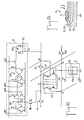
- the retina illustrated in FIG. 1 is constituted by a network of identical cells 10 integrated on the same substrate and interconnected.
- Each cell 10 comprises a photosensitive element 11.
- This can be constituted by a photodiode which in NMOS technology, is for example produced by N + scattering in the substrate P- (FIG. 3). It is known in fact that such diffusions, even through the passivation layer (Si0 2 ), constitute vertical photo-diodes.
- the photo-diodes 11 are materialized by using the N + conductive layers formed in the substrate to connect the cells together, as will be described later.
- the photodiode 11 is shown with, in parallel, a current source 11a and a stray capacitance 11b, between the ground and a connection point A.
- the current of the source 11a is the leakage current of the parasitic capacity 11b.
- the intensity of the leakage current is a function in particular of the intensity of illumination of the photodiode.
- the charge level of the capacitor Ilb that is to say the voltage at point A, is representative of the value of the picture element which is projected on the surface of the retina at the location of the diode.
- the voltage at point A is applied to an analog-digital conversion and storage circuit comprising an inverter 11 connected between point A and a connection point B, two transistors T1, T2 whose output circuits are connected respectively between point B and a connection point C and between point A and a connection point D and a second inverter 12 connected between point C and point D.
- the inverter 11 constitutes an analog-digital converter element transforming the voltage at point A into binary information taking the value "0" or the value "1" depending on whether the voltage at point A is higher or lower than the operating threshold of the inverter. Pixel binarization is therefore performed by thresholding.
- the thresholding can, if necessary, be non-uniform over the entire retina. This is achieved by giving different sensitivities to the binarization photodiodes-inverters according to their location in the retina.
- Several means can be used for this purpose such as, for example, a selective masking of the photosensitive zones, a differentiation of the precharging voltages of the stray capacitances, a differentiation of the thresholds of the converters (differentiation of the inverters 11 formed on the substrate), or even a modulation of exposure times.
- the inverters 11, 12 constitute, with the transistors T1, T2, a circuit for memorizing the binary information obtained by conversion of the voltage at point A. Memorization is obtained by copying the information through the inverters 11, 12, by alternating switching of the transistors T1, T2 controlled by the signals t1, t2.
- the storage circuits of the cells 10 are organized in a two-dimensional network of shift registers.
- the cells are connected, in lines, by transistors S1, S2 which connect, respectively, the points B and A of a cell to the points C and D of the neighboring cell on the right and, in columns, by transistors V1, V2 which connect points D and C of a cell, respectively, to points A and B of the neighboring cell below.
- the transfer of information from one cell to another is controlled by means of control signals s1, s2, t1, t2, v1, v2 applied to the transistors S1, S2, T1, T2, V1 and V2.
- a shift to the right is controlled by closing S1 and T2, a shift to the left by closing T1 and S2, a shift upwards by closing V2 and T1, a shift downwards by closing T1 and V1, a shift diagonally down and to the right by closing S1 and V1 and an offset diagonally up and to the left by closing V2 and S2.
- each cell 10 comprises an elementary processor 12 integrated on the same substrate.
- Clock signals 01, 02, 03, 04 and a data signal e2 are applied in parallel to the various processors by means of control and data conductors formed on the substrate.
- Each processor 12 also receives, on a second data input, the information e1 stored in the cell storage circuit and available at point B.
- a data output from processor 12 is connected by a transistor Ts at point C of the storage circuit in order to be able to write, in the latter, the information representing the result of the processing carried out by the processor.
- the closing of the transistor Ts is controlled by a signal 0s.
- the integrated retina according to the invention is particularly suitable for the implementation of local combinatorial processing algorithms (TCL).
- TCL local combinatorial processing algorithms
- TCL local combinatorial processing algorithms
- Each of these elementary processing operations generally comprises a sequence of Boolean operations involving the binary information representing the pixel to be processed, the binary information representing the neighboring pixels and binary data representing predetermined thumbnails as a function of a reason to recognize or locate in the image to be processed.
- Each of these binary data is sent to the different cells to perform the desired treatments in parallel in the different cells, the image being shifted in front of the network of processors as a function of these treatments, by controlling the shift registers as appropriate.
- each processing the result for each pixel is written in the corresponding storage circuit, for possible further processing.
- each image is transformed successively on itself.
- the massive and natural parallelism of execution of the TCL algorithms on all the pixels of the image at the same time offers great processing power and speed.
- the information is extracted line by line, at the edge of the retina, by controlling the shift registers.
- the binary values are, for each column, available on the output terminals S1, S2, S3, ... in order to be serialized and memorized for further processing.
- a comparator 12a formed by a NON-EXCLUSIVE gate, receives the signals el and e2 and at its output connected by a transistor T01 to an input of an AND gate 12b with two inputs.
- the output of the gate 12b is connected, on the one hand, to the second input thereof and, on the other hand, by a transistor T03, to an input of an OR gate 12c with two inputs.
- the output of the gate 12c is connected to the second input of the latter and constitutes the data output of the processor 12.
- Transistors T02 and T04 controlled by the signals 02 and 04 are connected respectively between the output of the gate 12b and a point at high logic level (1) and between the output of gate 12c and earth (level 0).
- Transistors T01 and T03 are controlled by signals 01 and 03.
- the comparator 12a performs comparisons between data values e2 and the values e1 representing the pixel of the corresponding cell, or that of a neighboring cell after shifting the information.
- a processing phase consisting of a combination of a thumbnail with the image formed on the retina includes a series of comparisons between the pixels of the thumbnail and those occupying the same relative positions in the image.
- the output of AND gate 12b is initialized to 1 (closing of T02).
- the results of successive comparisons for processing a thumbnail are transmitted to gate 12b by successive closings of T01.
- the output of gate 12b remains at 1, but as soon as a result is negative (output of comparator at 0), the output of gate 12b changes to 0 and remains there until the end of the series of comparisons corresponding to the processing of the thumbnail, since this output is looped back into input.
- the buddy OR 12c has its output initialized to 0 by the closing of T04. At the end of each series of comparisons, the output of gate 12b is connected to the first input of gate 12c by closing transistor T03. If during the processing of several thumbnails, the output of the gate 12b is at 1 at the end of at least one series of comparisons (signifying recognition of the pattern of one of the thumbnails in the image formed on the retina), the output of the gate 12c goes to 1 and remains there because of its loopback at the input.
- FIG. 2 the production of the elementary processor, the block diagram of which is shown in FIG. 4, requires a low number of transistors, making integration very easy in each cell in the retina.
- the end of the exposure of the image corresponds to the instant of the first comparison of the binary information e1 with a data e2 since then the memory circuit is loaded with the binary information of a cell neighbor (offset).
- the retina according to the invention also allows operations other than the TCL algorithms.
- a displacement detection can be carried out by exposing an image, by reversing it, by re-exposing it and by detecting the existence of pixels of value 1 in the image obtained. It is also possible to load the retina with a non-blank image introduced line by line by acting on the shift registers.
Landscapes
- Engineering & Computer Science (AREA)
- Physics & Mathematics (AREA)
- Multimedia (AREA)
- Theoretical Computer Science (AREA)
- Nonlinear Science (AREA)
- General Physics & Mathematics (AREA)
- Signal Processing (AREA)
- Image Processing (AREA)
- Transforming Light Signals Into Electric Signals (AREA)
- Image Analysis (AREA)
- Image Input (AREA)
- Solid State Image Pick-Up Elements (AREA)
- Character Input (AREA)
Claims (7)
Applications Claiming Priority (2)
| Application Number | Priority Date | Filing Date | Title |
|---|---|---|---|
| FR8509256 | 1985-06-18 | ||
| FR8509256A FR2583602B1 (fr) | 1985-06-18 | 1985-06-18 | Retine integree a reseau de processeurs |
Publications (2)
| Publication Number | Publication Date |
|---|---|
| EP0211702A1 EP0211702A1 (de) | 1987-02-25 |
| EP0211702B1 true EP0211702B1 (de) | 1990-05-23 |
Family
ID=9320387
Family Applications (1)
| Application Number | Title | Priority Date | Filing Date |
|---|---|---|---|
| EP86401311A Expired - Lifetime EP0211702B1 (de) | 1985-06-18 | 1986-06-17 | Integrierte Netzhaut mit Prozessorennetz |
Country Status (5)
| Country | Link |
|---|---|
| US (1) | US4792982A (de) |
| EP (1) | EP0211702B1 (de) |
| JP (1) | JPH0795342B2 (de) |
| DE (1) | DE3671594D1 (de) |
| FR (1) | FR2583602B1 (de) |
Families Citing this family (18)
| Publication number | Priority date | Publication date | Assignee | Title |
|---|---|---|---|---|
| JPH07117380B2 (ja) * | 1986-07-18 | 1995-12-18 | アンリツ株式会社 | 受光変換装置 |
| US4921770A (en) * | 1988-08-04 | 1990-05-01 | Tetsuo Murayama | Photoreceptor for electrophotography |
| FR2641432B1 (fr) * | 1988-12-30 | 1995-07-21 | Thomson Csf | Dispositif integre d'acquisition et de traitement d'images |
| FR2656700B1 (fr) * | 1989-12-28 | 1992-08-07 | Aerospatiale | Procede de restitution du mouvement d'un mobile par observation d'un symbole forme sur ce dernier et dispositifs pour la mise en óoeuvre du procede. |
| US5086477A (en) * | 1990-08-07 | 1992-02-04 | Northwest Technology Corp. | Automated system for extracting design and layout information from an integrated circuit |
| US5754705A (en) * | 1990-11-02 | 1998-05-19 | Canon Kabushiki Kaisha | Image data compressing apparatus having a sensor size matching compression processing block size |
| FR2683348B1 (fr) * | 1991-11-06 | 1994-01-14 | Etat Francais Delegue Armement | Reseau bidimensionnel periodique de memorisation et de traitement booleen d'images. |
| WO1993025005A1 (en) * | 1992-05-22 | 1993-12-09 | Indiana University Foundation | Area-efficient implication circuits for very dense lukasiewicz logic arrays |
| US5262632A (en) * | 1992-05-29 | 1993-11-16 | International Business Machines Corporation | Integrated circuit for achieving pattern recognition |
| JPH0652319A (ja) * | 1992-05-29 | 1994-02-25 | Internatl Business Mach Corp <Ibm> | イメージ分析装置 |
| JPH09511078A (ja) * | 1993-12-12 | 1997-11-04 | エーエスピー ソルーション ユーエスエイ インコーポレイション | 信号処理方法および装置 |
| US6067368A (en) * | 1996-01-26 | 2000-05-23 | Authentec, Inc. | Fingerprint sensor having filtering and power conserving features and related methods |
| JP2980063B2 (ja) * | 1997-06-10 | 1999-11-22 | 三菱電機株式会社 | 画像処理装置 |
| EP1038259B1 (de) | 1997-12-18 | 2003-04-09 | Infineon Technologies AG | Vorrichtung zur bilderfassung |
| JP4458678B2 (ja) | 1998-10-07 | 2010-04-28 | 浜松ホトニクス株式会社 | 高速視覚センサ装置 |
| US6461562B1 (en) | 1999-02-17 | 2002-10-08 | American Scientific Materials Technologies, Lp | Methods of making sintered metal oxide articles |
| GB2398446B (en) * | 2003-02-12 | 2006-06-07 | Snell & Wilcox Ltd | Image processing |
| FR2934391B1 (fr) * | 2008-07-23 | 2010-08-27 | Ecole Nale Sup Artes Metiers | Circuit de traitement de donnees a processeur elementaire, ensemble de tels circuits, et capteur matriciel associe |
Family Cites Families (5)
| Publication number | Priority date | Publication date | Assignee | Title |
|---|---|---|---|---|
| US3683193A (en) * | 1970-10-26 | 1972-08-08 | Rca Corp | Bucket brigade scanning of sensor array |
| JPS5856363A (ja) * | 1981-09-30 | 1983-04-04 | Hitachi Ltd | 受光素子 |
| JPS5932250A (ja) * | 1982-08-16 | 1984-02-21 | Fuji Xerox Co Ltd | 原稿読取装置 |
| DE3236073A1 (de) * | 1982-09-29 | 1984-03-29 | Siemens AG, 1000 Berlin und 8000 München | Zweidimensionaler halbleiter-bildsensor mit einer anordnung zur reduzierung des ueberstrahlens |
| FR2539529B1 (fr) * | 1983-01-17 | 1987-08-21 | Dassault Electronique | Procede pour le traitement d'informations binaires et processeur pour la mise en oeuvre de ce procede |
-
1985
- 1985-06-18 FR FR8509256A patent/FR2583602B1/fr not_active Expired
-
1986
- 1986-06-17 US US06/875,078 patent/US4792982A/en not_active Expired - Fee Related
- 1986-06-17 EP EP86401311A patent/EP0211702B1/de not_active Expired - Lifetime
- 1986-06-17 DE DE8686401311T patent/DE3671594D1/de not_active Expired - Lifetime
- 1986-06-18 JP JP61143977A patent/JPH0795342B2/ja not_active Expired - Lifetime
Also Published As
| Publication number | Publication date |
|---|---|
| EP0211702A1 (de) | 1987-02-25 |
| FR2583602B1 (fr) | 1988-07-01 |
| DE3671594D1 (de) | 1990-06-28 |
| JPH0795342B2 (ja) | 1995-10-11 |
| JPS626384A (ja) | 1987-01-13 |
| US4792982A (en) | 1988-12-20 |
| FR2583602A1 (fr) | 1986-12-19 |
Similar Documents
| Publication | Publication Date | Title |
|---|---|---|
| EP0211702B1 (de) | Integrierte Netzhaut mit Prozessorennetz | |
| EP0052035B1 (de) | Dezentralisierte Zugriffsanordnung für verschiedene Datenverarbeitungseinheiten in einem Multiprozessorsystem | |
| FR2472784A1 (fr) | Matrice de traitement de donnees en parallele, notamment pour l'analyse d'images prises par un satellite | |
| FR2566219A1 (fr) | Procede et dispositif pour l'exploration d'une fenetre de la zone image d'un dispositif a transfert de charges du type a transfert de trames | |
| FR2743462A1 (fr) | Dispositif de lecture de barrettes de detecteurs avec effet tdi | |
| EP0115225B1 (de) | Verfahren zur Abtastung eines nach dem Zwischenspaltenprinzips wirkenden Bildsensors und Anordnung zur Durchführung des Verfahrens | |
| CH688425A5 (fr) | Circuit électronique organisé en réseau matriciel de cellules. | |
| EP0114768B1 (de) | Lichtempfindliche Ladungstransfervorrichtung | |
| EP0298002A1 (de) | Transpositionsspeicher für eine Datenverarbeitungsschaltung | |
| EP0039635A1 (de) | Zentralisiertes Zuteilungsverfahren und zentraler Arbiter | |
| FR2654283A1 (fr) | Dispositif de mise au point automatique pour un systeme optique. | |
| EP0540402B1 (de) | Netzwerk binärer Widerstände und dessen Gebrauch für die Etikettierung von verbündenen Komponenten numerischer Bilder | |
| FR2593634A1 (fr) | Dispositif a transfert de charges anti-bruit et procede de fonctionnement | |
| FR2532777A1 (fr) | Circuit de translation de signaux | |
| EP1976265B1 (de) | Bildsensor, der in der Lage ist, in einem Modus unter der Normauflösung zu funktionieren | |
| EP0680015B1 (de) | Pixelzuführgerät einer Kompressionsschaltungsoperatorsequenz sich bewegender Bilder | |
| EP0640910B1 (de) | Verfahren zur Steuerung einer FIFO-Schaltung und Einrichtung zu seiner Durchführung | |
| EP2188810A2 (de) | Speicherpunkt eines statischen speichers und anwendung für einen bildsensor | |
| FR2566162A1 (fr) | Dispositif memoire d'image analogique utilisant le transfert de charge | |
| FR2683348A1 (fr) | Reseau bidimensionnel periodique de memorisation et de traitement booleen d'images. | |
| EP0949761B1 (de) | Verfahren und Vorrichtung zur Bearbeitung von binären Daten | |
| FR2627876A1 (fr) | Dispositif de traitement parallele d'informations | |
| FR2538200A1 (fr) | Procede d'analyse d'un dispositif photosensible a transfert de ligne et dispositif de mise en oeuvre d'un tel procede | |
| FR2563035A1 (fr) | Dispositif de formation et de memorisation d'image a semi-conducteur | |
| FR3115145A1 (fr) | Dispositif d'acquisition d'une image 2d et d'une image de profondeur d'une scene |
Legal Events
| Date | Code | Title | Description |
|---|---|---|---|
| PUAI | Public reference made under article 153(3) epc to a published international application that has entered the european phase |
Free format text: ORIGINAL CODE: 0009012 |
|
| AK | Designated contracting states |
Kind code of ref document: A1 Designated state(s): DE GB IT NL |
|
| 17P | Request for examination filed |
Effective date: 19870725 |
|
| 17Q | First examination report despatched |
Effective date: 19890807 |
|
| GRAA | (expected) grant |
Free format text: ORIGINAL CODE: 0009210 |
|
| AK | Designated contracting states |
Kind code of ref document: B1 Designated state(s): DE GB IT NL |
|
| ITF | It: translation for a ep patent filed | ||
| GBT | Gb: translation of ep patent filed (gb section 77(6)(a)/1977) | ||
| REF | Corresponds to: |
Ref document number: 3671594 Country of ref document: DE Date of ref document: 19900628 |
|
| PLBE | No opposition filed within time limit |
Free format text: ORIGINAL CODE: 0009261 |
|
| STAA | Information on the status of an ep patent application or granted ep patent |
Free format text: STATUS: NO OPPOSITION FILED WITHIN TIME LIMIT |
|
| 26N | No opposition filed | ||
| PGFP | Annual fee paid to national office [announced via postgrant information from national office to epo] |
Ref country code: GB Payment date: 19930611 Year of fee payment: 8 |
|
| PGFP | Annual fee paid to national office [announced via postgrant information from national office to epo] |
Ref country code: DE Payment date: 19930621 Year of fee payment: 8 |
|
| ITTA | It: last paid annual fee | ||
| PGFP | Annual fee paid to national office [announced via postgrant information from national office to epo] |
Ref country code: NL Payment date: 19930630 Year of fee payment: 8 |
|
| PG25 | Lapsed in a contracting state [announced via postgrant information from national office to epo] |
Ref country code: GB Effective date: 19940617 |
|
| PG25 | Lapsed in a contracting state [announced via postgrant information from national office to epo] |
Ref country code: NL Effective date: 19950101 |
|
| GBPC | Gb: european patent ceased through non-payment of renewal fee |
Effective date: 19940617 |
|
| NLV4 | Nl: lapsed or anulled due to non-payment of the annual fee | ||
| PG25 | Lapsed in a contracting state [announced via postgrant information from national office to epo] |
Ref country code: DE Effective date: 19950301 |
|
| PG25 | Lapsed in a contracting state [announced via postgrant information from national office to epo] |
Ref country code: IT Free format text: LAPSE BECAUSE OF NON-PAYMENT OF DUE FEES;WARNING: LAPSES OF ITALIAN PATENTS WITH EFFECTIVE DATE BEFORE 2007 MAY HAVE OCCURRED AT ANY TIME BEFORE 2007. THE CORRECT EFFECTIVE DATE MAY BE DIFFERENT FROM THE ONE RECORDED. Effective date: 20050617 |