EP0212499A2 - Informationsverarbeitungsanlage mit einem Allzweckprozessor und einem Sonderzweckprozessor - Google Patents
Informationsverarbeitungsanlage mit einem Allzweckprozessor und einem Sonderzweckprozessor Download PDFInfo
- Publication number
- EP0212499A2 EP0212499A2 EP86110992A EP86110992A EP0212499A2 EP 0212499 A2 EP0212499 A2 EP 0212499A2 EP 86110992 A EP86110992 A EP 86110992A EP 86110992 A EP86110992 A EP 86110992A EP 0212499 A2 EP0212499 A2 EP 0212499A2
- Authority
- EP
- European Patent Office
- Prior art keywords
- data
- purpose processor
- processor
- general purpose
- special purpose
- Prior art date
- Legal status (The legal status is an assumption and is not a legal conclusion. Google has not performed a legal analysis and makes no representation as to the accuracy of the status listed.)
- Granted
Links
Images






Classifications
-
- G—PHYSICS
- G06—COMPUTING OR CALCULATING; COUNTING
- G06F—ELECTRIC DIGITAL DATA PROCESSING
- G06F9/00—Arrangements for program control, e.g. control units
- G06F9/06—Arrangements for program control, e.g. control units using stored programs, i.e. using an internal store of processing equipment to receive or retain programs
- G06F9/30—Arrangements for executing machine instructions, e.g. instruction decode
- G06F9/38—Concurrent instruction execution, e.g. pipeline or look ahead
- G06F9/3885—Concurrent instruction execution, e.g. pipeline or look ahead using a plurality of independent parallel functional units
- G06F9/3889—Concurrent instruction execution, e.g. pipeline or look ahead using a plurality of independent parallel functional units controlled by multiple instructions, e.g. MIMD, decoupled access or execute
-
- G—PHYSICS
- G06—COMPUTING OR CALCULATING; COUNTING
- G06F—ELECTRIC DIGITAL DATA PROCESSING
- G06F9/00—Arrangements for program control, e.g. control units
- G06F9/06—Arrangements for program control, e.g. control units using stored programs, i.e. using an internal store of processing equipment to receive or retain programs
- G06F9/30—Arrangements for executing machine instructions, e.g. instruction decode
- G06F9/38—Concurrent instruction execution, e.g. pipeline or look ahead
- G06F9/3877—Concurrent instruction execution, e.g. pipeline or look ahead using a secondary processor, e.g. coprocessor
- G06F9/3879—Concurrent instruction execution, e.g. pipeline or look ahead using a secondary processor, e.g. coprocessor for non-native instruction execution, e.g. executing a command; for Java instruction set
-
- G—PHYSICS
- G06—COMPUTING OR CALCULATING; COUNTING
- G06F—ELECTRIC DIGITAL DATA PROCESSING
- G06F9/00—Arrangements for program control, e.g. control units
- G06F9/06—Arrangements for program control, e.g. control units using stored programs, i.e. using an internal store of processing equipment to receive or retain programs
- G06F9/44—Arrangements for executing specific programs
- G06F9/448—Execution paradigms, e.g. implementations of programming paradigms
- G06F9/4494—Execution paradigms, e.g. implementations of programming paradigms data driven
Definitions
- the present invention relates to an information processing apparatus of a dual processor system having a general purpose processor and a special purpose processor.
- Microcomputers includes a general purpose processor which is designed according to standard microcomputer architecture and used in many application fields.
- a general purpose processor which is designed according to standard microcomputer architecture and used in many application fields.
- a dual processor system is usually employed, wherein the general purpose processor is used as a host processor to control a processing sequence or a processing flow of a system.
- a specific processing is usually required in the system.
- Numeric processing, transaction processing and data transmission processing are enumerated as the specific processing. Further, the specific processing must be performed at high speed in real time operation. In addition, a large amount of data is to be manipulated in the specific processing. Therefore, the special purpose processor is used to perform the specific processing in a required program.
- a numeric processor or an I/O processor is known as the special purpose processor and is used as a co-processor or a slave-processor in the dual processor system.
- the conventional special purpose processors are all designed according to the von Neumann architecture. That is, the special-purpose co-processor or slave-processor is basically similar to the general purpose processor.
- the special purpose processor is different from the general purpose processor only in an arithmetic operation function or in an input-output function.
- one of the special purpose processors is designed so as to be applied to an arithmetic operation of variable bit length.
- an arithmetic logic unit (ALU) with a long bit length is employed.
- the other special purpose processor contains two ALUs for executing a floating-point operation.
- these processors require a long period of time to perform the above-mentioned specific processing, with the operating timing different from that of the general purpose processor. Therefore, the general purpose processor must always supervise the operation of the special purpose processor, so that the general purpose processor can not execute the required program when the special purpose processor is executing the specific processing.
- the special purpose processor is basically designed according to the stored program architecture as described above and the required specific processing can not be enabled until all of the data to be processed are entered into the special purpose processor. For example, if A x B + C x D is to be executed as the specific processing, the special purpose processor can not start the calculation until all the four data, A, B, C and D are entered thereinto. If the data C and D are entered into the special purpose processor earlier than the entry of the data A and B, the calculation can not be started until both the data A and B are entered. These data A, B, C and D are entered into the special purpose processor under the control of the general purpose processor. Therefore, the queuing time in the special purpose processor becomes long, so that the performance of the special purpose processor is reduced.
- the special purpose processor requires a complex ALU with a large size and therefore can not be formed on the same chip of the general purpose processor.
- the conventional dual processor system includes separate chips of the special purpose processor and the general purpose processor. Further, the two chips are associated by means of a connection whose dimensions are by no means negligible as compared with the size of the two chips and associating them militates against satisfying the criterion of small size.
- a complex interface circuit is required to arbitrate a bus coupling between the general purpose processor and the special purpose processor.
- Another object of the present invention is to provide an information processing apparatus wherein both a general purpose processor and the special purpose processor can be formed on a single semiconductor chip.
- Another object of the present invention is to provide an information processing apparatus of a dual processor system suitable for a high-speed operation or a real time operation.
- Still another object of the present invention is to provide an improved special purpose processor which can be used as co-processor or slave processor.
- An information processing apparatus of the present invention has a general purpose processor and a special purpose processor, characterized in that a data flow processor is used as the special purpose processor and is designed according to pipeline control architecture with a token ring bus.
- the general purpose processor prepares a plurality of token, each token having a sequence control information and a data to be processed, and supplies each token to the data flow processor as a co-processor or a slave-processor in a random order through a bus coupling the general purpose processor to the data flow processor.
- the data flow processor handles data inputted in a random and unscheduled manner on the basis of the sequence control information of the supplied token according to the data flow sequence.
- the data flow processor executes a required special processing asynchronous with the operation of the general purpose processor, so that the general purpose processor need not supervise the processing status of the special purpose processor and may execute a given program in parallel with the special processing in the data flow processor.
- the data flow processor as the special purpose processor sends a data transfer request signal to the general purpose processor after the special processing has been terminated and sends the result of the special processing to the general purpose processor in response to a data transfer acknowledge signal which is returned from the general purpose processor.
- the general purpose processor can operate the program independent of the special processing when the special purpose processor executes the special processing. Further, the general purpose processor can randomly supply unscheduled tokens to the special purpose processor. Thus, a queuing time of data to be processed can be remarkably reduced.
- the data flow processor of the present invention is featured in that the data and the sequence control information contained in each token are separately stored in different first and second memories, respectively.
- the first memory is used to store the data only, while the second memory is used to store the sequence control information only. Further, the first memory contains two storage areas; that is, a source data area and a destination data area. A pair of a source data and a destination data is required to execute a dyadic operation.
- the first memory further has a first flag portion, while the second memory has a second flag portion. The first flag portion stores "1" when the corresponding source data is stored in the source data area, while the second flag portion stores "1" when the corresponding destination data is stored in the destination data area.
- the data of each token is classified and stored in either the source data area or the destination data area according to a source/destination designating bit included in the sequence control information in each token.
- the first memory is used as a queue memory.
- both the source flag portion and the destination flag portion are "1”
- the source data and the destination data are simultaneously read out from the same address.
- either the source flag portion or the destination flag portion is "0”
- the first memory does not perform a read operation.
- the dyadic operation is accurately executed according to the source and destination flag bits.
- an interface control between the general purpose processor and the special purpose processor is simplified and is performed without any complex hardware means. Further the special purpose processor requeres neither complex arithmetic means nor complex input/output means. Therefore, the special purpose processor can be easily formed on the same chip as the general purpose processor chip.
- a conventional single-chip microcomputer A comprises a central processing unit (CPU) 100, a peripheral I/O control circuit 101, a program memory (ROM) 102, a data memory (RAM) 103 and an internal bus 104.
- the CPU 100 includes a program counter 100-1 (hereinafter called “PC"), a program status word register (hereinafter called "PSW") 100-2, a general purpose register set 100-3 and an interrupt control circuit 100-4.
- the interrupt control circuit 100-4 accepts an interrupt request signal 101-1 from the peripheral I/O control circuit 101 and controls the interrupt processing of the CPU 100.
- the program memory 102 stores an interrupt execution command and commands for a required program and the data memory 103 stores data. They are connected to each other by the internal bus 104 which is coupled to an external bus 105.
- the CPU 100 reads out commands from the program memory 102 whose addresses are designated by the PC, and sequentially executes the commands.
- the input portion 101-1 of the peripheral I/O control circuit 101 is coupled to various sensors, while its output portion 101-2 is coupled to a utilization device such as a driving circuit for a motor.
- the peripheral I/O 101 informs the interrupt control circuit 100-4 of the occurrence of interruption by sending the interrupt request signal 101-1.
- the CPU 100 shelters the concurrent contents of PC 100-1, PSW 100-2 and the general purpose register set 100-3 to a stack area (not shown) and executes the specific processing corresponding to the interruption.
- the CPU 100 receives the data to be processed from the peripheral I/O control circuit 101, calculates the received data and outputs the result of calculation to the peripheral I/O 101.
- the CPU 100 returns the contents of the stack area into PC 100-1, PSW 100-2 and the general purpose register set 100-3, respectively, and restarts the main routine.
- each specific processing (the input/output processing and calculation processing)must be executed under the interruption operation.
- these specific processings must be executed at a high speed or as a real time operation and a large amount of data must be processed.
- the dual chip processor system has a general purpose processor chip (GPP) 200 and the special purpose processor chip (SPP) 201 which are coupled to a common memory 202 containing a program and data via a common external bus 203. They receive simultaneously the same instruction from the memory 202 and decode it, respectively. If the instruction is to be used in the GPP 200, the general purpose processor 200 executes the instruction, while the SPP 201 cancels the instruction and enters a wait state. On the other hand, if it is to be used in the specific purpose processor chip 201, the processor 201 informs the general purpose processor 200 of the start of the specific processing by activating a signal 201-1 and thereafter executes the specific processing according to the instruction.
- GPP general purpose processor chip
- SPP special purpose processor chip
- the SPP 201 uses the common bus 203 to access the memory 202 for data read out from the memory 202 or data written into the memory 202 after sending a bus request signal 201-2 to the GPP 200 and receiving a bus grant signal 201-3 returned from the GPP 200.
- the conventional dual processor system shown in Fig. 2 can execute the general processing and the specific processing in the two processor chips, respectively.
- each instruction must be decoded simultaneously by the two processors, either processor cannot decode the instruction earlier than the other processor. This forces one processor to wait until the other processor terminates the concurrent processing.
- the general purpose processor 200 checks the signal 201-1 from the special purpose processor 201 and if the special purpose processor 201 is executing the special processing, it enters necessarily the waiting state. Accordingly, even if the processing capacity of each processor is high, a parallel processing is not performed.
- Fig. 3 shows an improved dual processor system in which the general purpose processor (GPP) 200 and the special purpose processor (SPP) 201 have their local memories 204, 205 connected to local buses 206, 207, respectively, and when the data exchange is to be made between both processors, they make access to the common memory 202 connected to the common bus 203 through a bus control unit 208.
- Both processors 200 and 201 orginarily execute the instruction by use of their own local buses 206, 207 and local memories 204, 205, and each processor makes access to the common memory 202 when the general purpose processor 200 delivers the data to be calculated to the special purpose processor 201 or when the special purpose processor 201 delivers the calculation result to the general purpose processor 200.
- the bus control unit 208 first receives the address information from the general purpose processor 200 and judges whether the memory to which access is made is the local memory 204 or the common memory 202. When the address is that of the common memory 202, competition of the special purpose processor 201 and the common bus 203 is checked. It the special purpose processor acquires the common bus 203 at that time with reading out the data from the common memory 202 and writing the data into the common memory 202, the bus control unit 208 makes active the bus hold signal 208-1 to the general purpose processor 200 and keeps the disconnection between the local bus 206 and the common bus 203.
- the general purpose processor 200 checks the bus hold signal 208-1 at a predetermined time interval and continues the waiting state until the signal becomes inactive.
- the bus control unit 208 connects the local bus 206 to the common bus 203 and the general purpose processor 200 can write the data into the common memory 202 through the common bus 203.
- the two processors shown in Fig. 3 can independently operate except for the period of access to the common memory and the system allows the parallel processing.
- this system has many drawbacks.
- the system itself is large in scale and a specific hardware such as the bus control unit 208 is necessary for controlling the common bus. Since the bus control unit 208 always judges the address every time the access is made to the memory, the access speed is low. Since data communication between the processors is made through an external common bus 203, a large quantity of power is necessary for driving the external common bus. In addition, when the data communication quantity between both processors becomes great, a bus neck occurs in the common bus, and the waiting state of one of the processors becomes a serious problem for improving the effect of parallel processing.
- the general purpose processor 200 as a host processor controls the peripheral devices (not shown) while the special purpose processor 201 as a co-processor executes numeric calculation for the data sent from the peripheral device.
- the local memory 205 of the processor 201 stores a plurality of calculation programs.
- the signals sent from the various sensors are inputted asynchronously to the general purpose processor 200 through the peripheral I/O control unit, and the general purpose processor 200 writes the data necessary for the calculation of the specific processing into the common memory 202 through the common bus 203.
- the special purpose processor 201 receives the data from the common memory, and starts the calculation after all the data to be calculated are prepared in the memory.
- the calculation result is written into the memory 202, and the general purpose processor 200 accesses the memory 202 and transfers the result to the peripheral device.
- the special purpose processor In the control field where the calculation processing of the asynchronous input data is primarily effected as described above, the special purpose processor has an extremely long waiting time by poring of the data to be calculated because it starts execution only after all the data are prepared for the calculation. Therefore, although parallel execution is possible, the working ratio of the special purpose processor is limited to a low level.
- a microcomputer in accordance with a first embodiment of the present invention comprises a general purpose processor (GPP) 1 for executing general processing among a required program, a special purpose processor (SPP) 2 for executing specific processing (e.g. numeric calculation processing) among the required program, a data memory 3 for storing processing data, a program memory 4 for storing instructions necessary to the processing of the program, and a peripheral input/output unit 5 coupled to at least one peripheral device (not shown). These units are connected to one another by a bus 6.
- the feature of the present invention is in the use of a data flow processor for the SPP 2.
- the general purpose processor 1 has a program counter used to read out instructions from the program memory 4 and controls sequentially the program flow. In response to such an instruction read out of the program memory 4 that is to be executed by the special purpose processor 2, the general purpose processor 1 produces a token by combining a sequence control information and data to be calculated and transfers the token to the special purpose processor 2 through the bus 6.
- the special purpose processor 2 contains a memory table in which a plurality of instructions are preliminarily stored, each instruction being prepared according to the minimum calculation unit of the monadic or dyadic operation.
- the processor 2 handles each calculation unit as the independent calculation task and executes the processing for each calculation task.
- the processor 2 is actuated by the token transferred thereto from the general purpose processor 1 via the bus 6.
- one calculation task is executed according to the corresponding instruction which is selected by the sequence control information contained in the token.
- the result of processing of the calculation task may be used as a new data of the next calculation task. In this manner, this procedure is sequentially executed by using a token ring bus.
- the special purpose processor 2 is designed according to the data flow (data driven) architecture and is used as co-processor or slave processor.
- T3 Since T3 is actuated after completion of execution of T1 and T2, it is subordinate in terms of time sequence, but it is irrelevant to T1 and T2 in relation to the data to be calculated because the data necessary for T3 are only A' and C' and it is not necessary for T3 to watch the execution state of T1 and T2 such as the input state of A, B, C and D, and the like. Accordingly, T1, T2 and T3 can be regarded as the mutually independent calculation tasks.
- calculation task T1 When the data A and B are transferred from the general purpose processor 1, the calculation task T1 is executed in the processor 2. Similarly, when the data C and D are transferred from the general purpose processor 1, the calculation task T2 is executed in the processor 2.
- the data A, B, C and D may be randomly entered into the processor 2, and the task T2 may be executed before the execution of the task T1. Only calculation task T3 is executed when A' and C' are prepared after completion of execution of T1 and T2.
- a large number of calculation programs consisting of a plurality of calculation tasks are preliminarily stored in the processor 102, and each calculation task is executed as soon as the data for it are prepared.
- the sequence control information in each token designates the calculation tasks for the data corresponding to each information, so that the data of each calculation task are mutually discriminated.
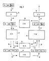
- FIG. 5 shows an internal block diagram of the special purpose processor 2, the function of the processor 2 will be described.
- the processor 2 contains the following seven units:
- the input interface unit 21 and the data transfer unit 27 are connected to the bus 6, while the other five units 22, 23, 24, 25 and 26 are connected in the ring form by token buses 28, 29, 30, 31, 32 and 33. Further, address buses 34 and 35 are used to couple the DLM 23 to the ACU 22 and TSCU 25, respectively.
- the interface unit (IU) 21 receives the token from the general purpose processor 1 and transfers the received token to the address calculation unit (ACU) 22 when the data bus 28 is empty.
- the address calculation unit (ACU) 22 calculates an address of the DLM 23 at which the data in the token is to be stored by use of the sequence control information in the token, outputs the address to the address bus 34 and transfers the data contained in the token to the data latch memory (DLM) 23 through the token bus 29. Further, the sequence control information caontained in the token and added with the calculated address is transferred to the FIFO type task queue memoty (TRQ) 24 through the parallel token bus 30.
- TRQ FIFO type task queue memoty
- the sequence control information arrived earliest at the TRQ 24 is firstly read out of the TRQ 24 and is transferred to the TSCU 25 via the token bus 32.
- the TSCU 25 accesses the DLM 23 according to the address produced by the ACU 22 and added to the sequence control information via the address bus 35.
- the data at the accessed address is read out of the DLM 23 and sent to the TSCU 35 through the parallel token bus 31.
- the data latch memory 23 examines whether or not the other data has already stored therein. If the other data has already presented in the data latch memory 23, the data latch memory 23 transfers both data to the TSCU 25 simultaneously. On the other hand, if the other data has not yet arrived at the data latch memory (DLM) 23, the accessed data is not transferred to the TSCU 25 and is retained therein, waiting for the arrival of the other data. At this time, the sequence control information is transferred as it is through the token buses 33, 28 and 30 and is entered into the TRQ 24 again.
- DLM data latch memory
- the data latch memory (DLM) 23 transfers the data to the TSCU 25 via the token bus 32 because the calculation task is in the ready state without waiting.
- the task sequence control unit (TSCU) 25 contains a memory table storing a plurality of calculation mode and designates the calculation mode to be executed according to the control information of the calculation task under the ready state.
- the data to be calculated are transferred to the execution unit (EXU) 26 through the token bus 23.
- the execution unit (EXU) 26 transfers the data as the final calculation result to the data transfer unit (DTU) 27 through the bus 33.
- the execution unit (EXU) 26 executes the calculation processing designated by the calculation mode supplied from the TSCU 25.
- the EXU 26 constitutes the token by the sequence control information updated by the task sequence control unit 25 and transfers the token to the address calculation unit 22 through the token bus 28.
- the data transfer unit (DTU) 27 receives the final calculation result from the task sequence control unit 25 and informs the termination of the processing to the general purpose processor 1.
- the general purpose processor 1 transfers the final calculation result to the data memory 3 through the bus 6.
- a plurality of tokens inputted from the general purpose processor 1 are calculated in accordance with a plurality of calculation tasks with queuing operation.
- the general purpose processor 1 can enter randomly unscheduled data into the special purpose processor 2.
- the calculation result is produced in the processor 2.
- Fig. 6 is an internal block diagram of the general purpose processor 1.
- the processor 1 is basically designed according to von Neumann architecture in this embodiment and contains a program memory (ROM) 36 storing instructions for processing a required program, a program counter (PC) 37 to read instructions out of the ROM 36 sequentially, a queue memory 38 used as an instruction register, a micro-sequencer 39 storing microprograms, an instruction decoder 40 decoding instructions, an arithmetic and logic unit (ALU) 41, a temporary register 42 storing the result of ALU, a data memory (RAM) 43 containing a working register set, an address producing unit 44 and an I/O control unit 45.
- ROM program memory
- PC program counter
- the system bus 6 is coupled to a first internal bus 48 which is connected to ROM 36 and the queue memory 38.
- the queue memory 38 can receive an instruction from the external through the system bus 6 and the instruction in the ROM 36 can be transferred to the system bus 6.
- the I/O control unit 45 is coupled to the bus 6 via the first internal bus 48 and has a bus control function as well as a data transfer function.
- the processor employs a dual bus structure with two buses 49 and 50 separately provided.
- the RAM 43 of a dual-port type is coupled to both buses 49 and 50.
- the dual buses 49 and 50 are coupled to the first internal bus 48 and a second internal bus 51 via buffers 46 and 47, respectively.
- sequence control information and the data to be calculated are produced and are transferred to the special purpose processor 2 as a token.
- the sequence control information may be transferred to the system bus 6 through the internal buses 50 and 51, and the data may be transferred to the system bus 6 through the internal buses 49 and 48.
- the sequence control information and the data may be transferred to the system bus 6 in serial via the bus 48.
- a bus 52 is provided to connect the bus 51 to the bus 48.
- the general purpose processor 1 can be coupled to the data flow type special purpose processor 2 according to a normal bus coupling technique.
- the processor 1 prepares the sequence control information containing a table address (TA), a data base pointer (DBP), a source/destination designating bit (S/D), a data length code (DL) and a data format code (DF).
- the table address (TA) and the data base pointer (DBP) are produced by the address producing unit 44 and used in the address calculation unit (ACU) 22 in the special purpose processor 2 for producing the address to access the DLM 23.
- the S/D is used to indicate that the data to be calculated in the processor 2 is whether the source data or the destination data. For example, when the S/D is "1", the data is manipulated as the source data, while when the S/D is "0", the data is manipulated as the destination data.
- the data length code (DL) indicates the number of bytes of the data to be calculated. When the data consists of one byte, the DL is "00", while the DL is "01" for the data consisting of two bytes. It is "10" for the data of three bytes.
- the code of DL may be arbitrarily prepared according to the data to be processed.
- the data format code DF represents as shown in Table 1.
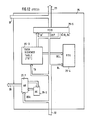
- Flow of the sequence control information (TA, DBP, S/D, DL and DF) in the processor 2 will be now explained with reference to Figs. 7 to 14. It is first entered into the input interface unit 21 in Fig. 7 through the system bus 6 and is stored in a data buffer (DB) 21-1 therein shown in Fig. 8. The DL among the sequence control information is further entered into a timing controller (TC) 21-2 (Fig. 8). The timing controller 21-2 controls entry of the data according to the DL. That is, when the DL is "01", the TC 21-2 controls the DB 21-1 so as to store two bytes of the data. The byte is transferred one by one.
- TC timing controller
- the sequence control information is transferred to the address calculation unit (ACU) 22 shown in Fig. 9 through the bus 28.
- the information is stored in a tag data buffer (TDB) 22-1.
- the table address (TA) is applied to a data address table (DAT) 22-2 as an address.
- the DAT 22-2 has a data and a control code (CTL).
- the data is applied to an adder (ADD) 22-3 together with the data base pointer (DBP).
- the result of the addition is transferred to the address bus 34 coupled to the DLM 23 via an address buffer (AB) 22-5 as an effective address designating a location in which the data to be processed is stored.
- the effective address to be transferred to the DLM is also stored in the TDB 22-1 as a data storage address (DSA).
- the CTL is transferred to the DLM 23 through the bus 29 and indicates a processing task function as shown in Table 2.
- the S/D bit is also transferred to the DLM 23 through the bus 29 to indicate either the source data or the destination data.
- the data format (DF) shown in table 1 is applied to a timing controller (TC) 22-4 to indicate predetermined timing operation according to the designated format.
- the sequence control information (TA, DBP, DSA and DL) is transferred to the task queue memory (TRQ) 24 through the bus 30.
- the data to be processed is directly transferred from the bus 28 through the bus 29 to the DLM 23 together with the CTL and S/D.
- the task queue memory 24 has a tag data queue (TDQ) 24-1 of a first-in first-out (FIFO) memory structure and a queue status controller (QSC) 24-2 as shown in Fig. 10.
- the sequence control information is entered into the TDQ 24-1 through the bus 30.
- the oldest sequence control information stored in the TDQ 24-1 is firstly derived therefrom and transferred to the task sequence control unit (TSCU) 25 through the bus 32.
- the queue status controller (QSC) 24-2 checks the status of the TDQ 24-1 and generates a queue overflow control signal (QSCC) when the TDQ 24-1 is filled with the entered information. That is, when the TDQ 24-1 has no empty memory area, an entry of a new sequence control information is stopped by the QSCC signal.
- QSCC queue overflow control signal
- the QSCC signal is applied to the timing controller (TC) 22-4 in the ACU 22 (Fig. 9) to stop output of the subsequent control information.
- TC timing controller
- Fig. 9 the entry into the TDQ 24-1 is inhibited until the information already stored in the TDQ 24-1 is derived therefrom.
- the data latch memory DLM 23 (Fig. 11) has a storage means including a source data area (SDA) 23-2 and a destination data area (DDA) 23-4, each of which has a plurality of storage locations. Each location has a flag bit. That is, the source data area contains a source flag bit V s 23-1 corresponding to each source data storage location, while the destination data area contains a destination flag bit V d 23-3 corresponding to each destination data storage location. Both areas are simultaneously accessed by either the address sent from the ACU 22 through the address bus 34 or the address sent from the TSCU 25 through the address bus 35. The address is decoded by an address decoder (AD) 23-5 to designate one of the common storage locations of the both areas SDA and DDA.
- AD address decoder
- the read-out V s and V d are applied to a memory controller (MC) 23-6 to which the CTL and S/D are also supplied from the bus 29.
- the memory controller (MC) 23-6 selects either one of SDA and DDA according to the S/D bit when the CTL 29 is "11". For example, when the S/D bit is "0", the SDA is selected and the data on the bus 29 is written at the location designated by the address. Further, the V s flag bit corresponding to the designated location is set. On the other hand, when the S/D bit is "1", the DDA is selected and the data is written at the location designated by the address. In addition, the V d flat bit corresponding to the designated location is set.
- the memory controller (MC) 23-6 further performs set or reset of the flag bit according to the CTL.
- the read address is applied from the address bus 35 to the AD 23-5 and both of V s and V d at the designated location are read out and supplied to the MC 23-6.
- both bits are set, the data in the SDA and DDA are both simultaneously read out and transferred to the TSCU 25 through the bus 31.
- the MC 23-6 checks the flag bits of V s and V d and enables the read operation only when both bits are set.
- the task sequence control unit (TSCU) 25 shown in Fig. 12 receives the control information consisting of TA, DBP, DSA and DL from the bus 32.
- the DSA which has been produced by the ACU 22 is supplied to an address buffer 25-1 and used to make access to the DLM 23 through the address bus 35.
- An address counter 25-2 is provided for the address buffer 25-1 for producing the sequential addresses to access the data of a plurality of bytes.
- the table address (TA) is supplied to a task sequence table (TST) 25-3 which produces a new table address (TA'), a new source/destination designating bit (S/D') and a new data length code (DL') to be used in a new sequence control information which in turn indicates a new processing with respect to the concurrent data if necessary and a selection code to be applied to a bus selector (BSL) 25-4.
- the bus selector 25-4 sends the data from the bus 31 to the execution unit 26 when the select code indicates the EXU 26 or to the data transfer unit (DTU) 27 when the select code indicates the DTU 27, that is, when the data processing is completed.
- the BSL 25-4 controls the data transfer according to the data length code (DL) supplied thereto.
- the execution unit (EXU) 26 (Fig. 13) has a sequencer 26-1 for indicating a calculation mode according to the control information, two registers 26-2 and 26-3, an arithmetic and logic unit (ALU) 26-4 and a latch 26-5.
- the ALU 26-4 executes a calculation (addition, subtraction, multiplication, division, comparison, etc.) according to the calculation mode indicated by the sequencer 26-1 and transfers the calculation result to the bus 28.
- the data transfer unit (DTU) 27 (Fig. 14) has a data buffer (DB) 27-1 coupled to the bus 33 at its input and to the system bus 6 at its output and temporarily storing the processing result, and a timing controller (TC) 27-2.
- DB data buffer
- TC timing controller
- the interface unit (IU) 21 in the special purpose processor 2 has the input data buffer (DB) 21-1 for storing the input token from the general purpose processor 1 while the data transfer unit (DTU) 27 has the output data buffer (DB) 27-1 for storing the processing result of the special purpose processor 2.
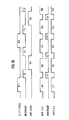
- the following control signals are used in order to control the communication between the general purpose processor 1 and the special purpose processor 2.
- the processor 1 applies a token transfer signal 60 which informs the processor 2 that the token is outputted to the bus 6.
- the signal 60 is generated by the peripheral control unit 45 in the GPP 1 and is received by the timing controller (TC) 21-2 of the IU 21.
- the timing controller 21-2 activates a signal 61 to inform the general purpose processor 1 that the interface unit 21 of the processor 2 cannot receive the token transferred from the general purpose processor 1.
- the TC 21-2 does not activate the signal 61.
- the processor 1 can acknowledge the token transfer according to the signal 61.
- the timing controller (TC) 21-1 activates the signal 61 when the QSCC signal is present but inactivates it when the QSCC signal is absent.
- the QSCC signal may be directly applied to the general purpose processor 1 as a signal 62 from the TRQ so as to directly inform the GPP 1 of such a status of the special purpose processor 2 that the TDQ has been filled and no more control information is accepted.
- the signal 61 can be omitted.
- the TC 27-2 when the processing result is stored in the data buffer 27-1 of the DTU 27, the TC 27-2 generates a data transfer request signal 63 which is applied to the peripheral control unit 45 of the processor 1.
- the processor 1 receives the processing result through the bus 6 when the data entry is acceptable by returning a grant signal 63. Though the request signal and the grant signal are transferred bidirectionally on the source signal line, these signals may be separated from each other. Further, the processing result may be sent directly to the data memory 3.
- the general purpose processor 1 fetches the instruction from the program memory 4 and when the instruction is judged to be such one that commands the specific processing to be executed by the processor 2, the general purpose processor 1 adds the sequence control information designating the calculation task to the data to be processed, whereby the token is prepared.
- the general purpose processor 1 then generates the token transfer signal 60, outputs the token to the bus 6 and checks the level of the signal 61 from the processor 2.
- the signal 61 is active, the general purpose processor 1 is under the waiting state while outputting the token to the bus 6, and repeatedly checks the signal 61.
- the signal 61 becomes inactive, it judges that the processor 2 receives the token, and fetches the next instruction from the program memory 4 to execute that instruction simultaneously with the execution of the specific processing by the processor 2.
- the processor 2 checks the state of the input buffer 21-1 in the interface unit 21, makes inactive the signal 61 when the input token buffer 21-1 is empty, and takes the token on the bus 6 into the input token buffer 21-1.
- the processor 2 keeps the signal 61 active until the interface unit 21 transfers the token to the address calculation unit 22.
- the general purpose processor 101 checks the state of the signal 62 from the processor 2. When the QSCC signal is present, the general purpose processor 1 suspends the transfer of the token to the processor 2 and executes other processings. After that, it transfers the token again to the processor 2 in the same way as the method described in the item (1) above.
- the general purpose processor 1 In connection with the transfer operation by the general purpose processor 1 of the calculation result of the processor 2 to the data memory 3, when the data transfer unit 27 in the processor 2 receives the final calculation result from the task sequence control unit 25, it requires the general purpose processor 1 to receive the calculation result by using the request signal 63. When accepting the request, the general purpose processor 1 temporarily stops the execution of the present program, receives the calculation result from the output data buffer 27-1 of the data transfer unit 27 and transfers it to the data memory 3 through the bus 6.
- the processor 2 waits for the calculation result thereinside irrespective of the transfer sequence of the data to be processed which is transferred from the general purpose processor 1, while the general purpose processor 1 need not at all consider the timing such as waiting in connection with the transfer sequence of the data to the processor 2 in order to establish the synchronous relation of the instruction execution sequence. Accordingly, the synchronous communication method of the instruction execution between the processor 1 and the processor 2 becomes simple. Further, the processor 2 can execute the input operation of the token, output operation of the calculation result and the calculation processing entirely independently of one another.
- the processor 2 can be formed on the same chip of the processor 1 together with the memories 3 and 4 and the peripheral I/O unit 5. Further, the present invention utilizes the processor of a data from (or driven) control type, in which an instruction is started upon data input, as the special purpose processor and can therefore provide the following advantages:
- the special purpose processor has therein a plurality of processing programs, and each program is divided into independent tasks so as to execute the processing in the task unit. Accordingly, a plurality of programs can be executed in parallel with one another. There does not exist fundamentally the execution sequence between a plurality of tasks, and those tasks are sequentially executed whose data are prepared. Accordingly, there is hardly any overhead such as the waiting for the input of the processing data.
- the speical purpose processor waits for the processing data thereinside in accordance with the sequence control information in the token irrespective of the transfer sequence of the processing data in the token transferred thereto from the general purpose processor and establishes the synchronous relation of the instruction execution sequence, the general purpose processor need not at all consider the timing such as waiting in connection with the transfer of the data to the special purpose processor. Accordingly, these general purpose processor have an extremely reduced overhead in conjunction with the transfer of the data to the special purpose processor.
- the present invention can remarkably improve the parallel processing efficiency of the dual processor system by reducing the overhead in connection with the data transfer between the processors.
- the conventional dual processor system in Fig. 2 requires different time periods for the processings G1, G2 in the GPP and those S1 and S2 in the SPP with intervals I1, I2, I3 used for data and information transfer.
- the GPP and the SPP can execute the respective processings G1, G2, ... and S1, S2 ... at the same time periods with intervals I1, I2 ... used for data and information transfer therebetween.
- the hardware resources can be utilized more effectively, and the single-chip microcomputer having an drastically improved processing capacity can be provided.
- the present invention provides great practical significance in accomplishing the high speed real time control particularly in the control field where parallel processing by multiprogramming is a requisite.
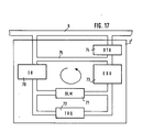
- Fig. 17 shows a block diagram of another embodiment of a numeric value calculation processor (special purpose processor) 2' for the data flow control.
- the numeric value calculation processor 2' contains an interface unit 70 which manages the state of the calculation task, a ready state task queue 72 which selectively stores the sequence control information of the token, a data latch memory 71 for storing the data to be calculated, an execution unit 73 for executing the calculation of the task, and a data transfer unit 74 for transferring the final calculation result.
- the interface unit 70, the ready state task queue 72, the data memory 71 and the execution unit 73 are connected to a token ring bus 75 in which the data move unidirectionally.
- the general purpose processor 1 addes predetermined control information to the calculation data to prepare the token, and transfers it to the interface unit 70 of the numeric calculation processor 2'.
- the interface unit 70 transfers the data among the inputted token to the data memory 71, decodes the control information, discriminates one of calculation tasks to be executed.
- the calculation task relating to the token is monadic calculation
- the calculation task enters the ready state upon receiving the data input, but in the case of the dyadic calculation, the counter-part data is first inputted to the numeric value calculation processor 2' and the interface unit 70 checks whether or not it is transferred to the data memory 71. As a result, if the counterpart data is found to have been transferred first to the data memory 71, the calculation task is under the ready state and if not, the input data wait for the counter-part data on the data memory 71.
- the interface unit 70 When the calculation task enters the ready state by the data input, the interface unit 70 generates the control information designating the calculation in the execution unit 73 and the storage address of the data memory for the calculation data, and transfers the information to the ready state task queue 72.
- the execution unit 73 receives the control information from the start of the ready state task queue 72 and the calculation data from the data memory 71 and calculates the task. After the calculation processing is complete, the execution unit 73 outputs the calculation result to the data transfer unit 74 when the calculation result is the final result to be delivered to the general purpose processor 1, or add the control information designating the next calculation task which uses the calculation result as its input data, to the calculation result and transfers it to the interface unit 70 when the calculation result is an intermediate result to the processing program.
- the data transfer unit 74 may transfer the calculation result to the data memory 3 through the bus 6.
- the DTU 74 may generate an interruption signal upon receipt of the final calculation result, to inform the general purpose processor 1 of the data transfer.
- the data inputted from the general purpose processor 1 moves on the ring bus 75 while waitng for the counterpart data on the data memory 71, as the calculation data of the predetermined calculation task, and is calculated at the execution unit 73.
- the calculation result is used as the input data for the next calculation task. This procedure is repeated while the data moves round the ring bus 75 a predetermined number of times, and the final calculation result is transferred by the data transfer unit 74 to the external data memory 3.
- the program memory 4 of the general purpose processor 1 stores the input/output processing program with the peripheral I/O unit 5, self-diagnosis program for fail-safe, and so forth, and a plurality of calculation processing programs for the asynchronous input data are written into the numeric value calculation processor 2' in the form of sequence of the calculation tasks.
- the peripheral I/O unit 5 When the data or signals are inputted from the various sensors to the peripheral I/O unit 5 (Fig. 4), the peripheral I/O unit generates the processing request to the general purpose processor 1.
- the general purpose processor 1 accepts this request and starts the corresponding processing routine.
- the general purpose processor 1 receives the data from the peripheral I/O unit 5 and if this input data requires the calculation processing with the asynchronous input data from other peripheral I/O unit 5, the general purpose processor 1 adds a predetermined tag data to the input data and transfers it to the numeric value calculation processor 2'. Then, it shifts to the next processing.
- the general purpose processor 1 repeats the operations of adding the predetermined tag data to the input data and transferring it to the numeric value calculation processor 2' in conjunction with the calculation processing of the asynchronous input data, but does not need the processing involving the overhead such as waiting for the data input of the counter-part calculation.
- the numeric value calculation processor 2' upon receiving the calculation data from the general purpose processor 1, the numeric value calculation processor 2' starts the calculation task while waiting for the counter-part data as described already, executes a plurality of instructions in parallel with one another and outputs the final calculation result to the data memory 3.
- the general purpose processor 1 reads out the calculation result written by the numerial calculation processor 2' from the data memory 3 and outputs it to the peripheral I/O unit 5.
- the general purpose processor 1 executes the data input/output processing with the peripheral I/O unit 5, the asynchronous input data transfer to the numeric value calculation processor and self-diagnosis processing of the system, while the numeric value calculation processor 2' executes the calculation processing of the asynchronous input data.
- both processors employ a clear function dispersion system.
- the present invention constitutes the function dispersion type dual processor system consisting of the general purpose processor and the numeric value calculation processor on the single semiconductor chip and employs the data flow control system for the numeric value calculation processor. Accordingly, the present invention can realize the single-chip microcomputer which can drastically reduce the effective calculation time of the numeric calculation processing of the asynchronous input data and can make real time control in the high end control field without using any particular hardwares for exclusive calculation purpose.
- the present invention constitutes the dual processor system on the single semiconductor chip without using any particular hardwares such as a bus arbiter, the present invention can reduce the package area and cost of production in the application system in comparison with the conventional 2-chip dual processor system, and can improve the system reliability.
- the on-chip dual processor system consisting of the general purpose processor and the numeric value calculation processor in accordance with the present invention provides a microcomputer system having extremely high cost performance and its practical utility is extremely high.
Landscapes
- Engineering & Computer Science (AREA)
- Software Systems (AREA)
- Theoretical Computer Science (AREA)
- Physics & Mathematics (AREA)
- General Engineering & Computer Science (AREA)
- General Physics & Mathematics (AREA)
- Multi Processors (AREA)
- Advance Control (AREA)
Applications Claiming Priority (4)
| Application Number | Priority Date | Filing Date | Title |
|---|---|---|---|
| JP17511785 | 1985-08-08 | ||
| JP175117/85 | 1985-08-08 | ||
| JP28878885 | 1985-12-20 | ||
| JP288788/85 | 1985-12-20 |
Publications (3)
| Publication Number | Publication Date |
|---|---|
| EP0212499A2 true EP0212499A2 (de) | 1987-03-04 |
| EP0212499A3 EP0212499A3 (en) | 1990-12-19 |
| EP0212499B1 EP0212499B1 (de) | 1993-12-15 |
Family
ID=26496480
Family Applications (1)
| Application Number | Title | Priority Date | Filing Date |
|---|---|---|---|
| EP86110992A Expired - Lifetime EP0212499B1 (de) | 1985-08-08 | 1986-08-08 | Informationsverarbeitungsanlage mit einem Allzweckprozessor und einem Sonderzweckprozessor |
Country Status (4)
| Country | Link |
|---|---|
| US (2) | US4860191A (de) |
| EP (1) | EP0212499B1 (de) |
| JP (1) | JP2564805B2 (de) |
| DE (1) | DE3689394T2 (de) |
Cited By (5)
| Publication number | Priority date | Publication date | Assignee | Title |
|---|---|---|---|---|
| GB2215878A (en) * | 1988-03-23 | 1989-09-27 | Benchmark Technologies | Chip-independant numeric subsystem |
| GB2261968A (en) * | 1991-11-26 | 1993-06-02 | Toshiba Kk | Cooperative distributed problem solver |
| EP0475028A3 (en) * | 1990-08-29 | 1993-11-10 | Siemens Ag | Procedure for operating a coprocessor in a distributed computer system |
| GB2392742A (en) * | 2002-09-04 | 2004-03-10 | Advanced Risc Mach Ltd | Synchronisation between pipelines in a data processing apparatus by using tokens |
| EP1271307A4 (de) * | 2000-03-03 | 2007-07-25 | Sony Computer Entertainment Inc | Kompatibles unterhaltungsgerät und computersystem |
Families Citing this family (90)
| Publication number | Priority date | Publication date | Assignee | Title |
|---|---|---|---|---|
| EP0576749B1 (de) * | 1992-06-30 | 1999-06-02 | Discovision Associates | Datenpipelinesystem |
| US5117489A (en) * | 1987-04-22 | 1992-05-26 | Mitsubishi Denki Kabushiki Kaisha | Data-driven processor having an internal tag-generating system for generating a distinct tagged information and assembling with un-tagged information of an input/output data packet |
| US5321845A (en) * | 1987-09-09 | 1994-06-14 | Hitachi, Ltd. | Single-chip microcomputer including non-volatile memory elements |
| JPS6481066A (en) * | 1987-09-24 | 1989-03-27 | Nec Corp | Connection system for multi-processor |
| US5115510A (en) * | 1987-10-20 | 1992-05-19 | Sharp Kabushiki Kaisha | Multistage data flow processor with instruction packet, fetch, storage transmission and address generation controlled by destination information |
| JPH0646414B2 (ja) * | 1987-10-20 | 1994-06-15 | シャープ株式会社 | 情報処理装置 |
| JPH01116733A (ja) * | 1987-10-30 | 1989-05-09 | Agency Of Ind Science & Technol | データフロー・プロセッサ |
| US5117499A (en) * | 1988-01-22 | 1992-05-26 | Sharp Kabushiki Kaisha | Data flow type processing apparatus having external and cache memories for fetching paired executing instruction when mishit occurs |
| US5257392A (en) * | 1988-01-29 | 1993-10-26 | Sharp Kabushiki Kaisha | System for loading and dumping data in a data flow processor based on paired program data and data to be processed |
| JPH01297764A (ja) * | 1988-05-25 | 1989-11-30 | Nec Corp | プロセッサ |
| JPH01303502A (ja) * | 1988-05-31 | 1989-12-07 | Fanuc Ltd | 数値制御装置 |
| US5214764A (en) * | 1988-07-15 | 1993-05-25 | Casio Computer Co., Ltd. | Data processing apparatus for operating on variable-length data delimited by delimiter codes |
| US5040109A (en) * | 1988-07-20 | 1991-08-13 | Digital Equipment Corporation | Efficient protocol for communicating between asychronous devices |
| WO1990001192A1 (en) * | 1988-07-22 | 1990-02-08 | United States Department Of Energy | Data flow machine for data driven computing |
| US5287450A (en) * | 1988-09-29 | 1994-02-15 | Mitsubishi Denki Kabushiki Kaisha | Video signal brancher |
| US5293586A (en) * | 1988-09-30 | 1994-03-08 | Hitachi, Ltd. | Data processing system for development of outline fonts |
| US5241635A (en) * | 1988-11-18 | 1993-08-31 | Massachusetts Institute Of Technology | Tagged token data processing system with operand matching in activation frames |
| US5497344A (en) * | 1989-01-26 | 1996-03-05 | Sharp Kabushiki Kaisha | Data flow type information processor |
| US5025390A (en) * | 1989-01-31 | 1991-06-18 | Staubli International Ag | Robotic workcell control system with a binary accelerator providing enhanced binary calculations |
| US5165036A (en) * | 1989-01-31 | 1992-11-17 | Sharp Kabushiki Kaisha | Parallel processing development system with debugging device includes facilities for schematically displaying execution state of data driven type processor |
| US5276893A (en) * | 1989-02-08 | 1994-01-04 | Yvon Savaria | Parallel microprocessor architecture |
| DE69031233T2 (de) * | 1989-02-24 | 1997-12-04 | At & T Corp | Adaptive Arbeitsfolgeplanung für Mehrfachverarbeitungssysteme |
| JP2668438B2 (ja) * | 1989-04-21 | 1997-10-27 | 三菱電機株式会社 | データ検索装置 |
| JP2559850B2 (ja) * | 1989-05-26 | 1996-12-04 | 三菱電機株式会社 | 制御用プロセッサ |
| JPH03154105A (ja) * | 1989-11-10 | 1991-07-02 | Toshiba Mach Co Ltd | Ncプログラム作成装置 |
| US5150470A (en) * | 1989-12-20 | 1992-09-22 | International Business Machines Corporation | Data processing system with instruction queue having tags indicating outstanding data status |
| EP0843254A3 (de) * | 1990-01-18 | 1999-08-18 | National Semiconductor Corporation | Integrierte, digital arbeitende Signalverarbeitungsanlage/Universalprozessor mit anteilig genutzten internem Speicher |
| US5028186A (en) * | 1990-01-29 | 1991-07-02 | Mechanical Plastics Corp. | Hollow wall anchor with enhanced holding strength |
| JPH03226883A (ja) * | 1990-01-31 | 1991-10-07 | Mitsubishi Electric Corp | 制御プロセッサ |
| US5305446A (en) * | 1990-09-28 | 1994-04-19 | Texas Instruments Incorporated | Processing devices with improved addressing capabilities, systems and methods |
| US5386537A (en) * | 1991-03-28 | 1995-01-31 | Minolta Camera Kabushiki Kaisha | System with reduced instruction set processor accessing plural memories at different speeds using bank interleaving |
| JP2582956B2 (ja) * | 1991-05-07 | 1997-02-19 | 三菱電機株式会社 | プログラマブル制御装置 |
| CA2074769C (en) * | 1991-08-09 | 2001-03-20 | International Business Machines Corporation | Formula processor |
| DE69228980T2 (de) * | 1991-12-06 | 1999-12-02 | National Semiconductor Corp., Santa Clara | Integriertes Datenverarbeitungssystem mit CPU-Kern und unabhängigem parallelen, digitalen Signalprozessormodul |
| JPH05181984A (ja) * | 1991-12-27 | 1993-07-23 | Sharp Corp | データ処理システム |
| IL100598A0 (en) * | 1992-01-06 | 1992-09-06 | Univ Bar Ilan | Dataflow computer |
| JPH0660015A (ja) * | 1992-06-08 | 1994-03-04 | Mitsubishi Electric Corp | 情報処理装置 |
| US6435737B1 (en) | 1992-06-30 | 2002-08-20 | Discovision Associates | Data pipeline system and data encoding method |
| US6330665B1 (en) | 1992-06-30 | 2001-12-11 | Discovision Associates | Video parser |
| US6047112A (en) * | 1992-06-30 | 2000-04-04 | Discovision Associates | Technique for initiating processing of a data stream of encoded video information |
| US6067417A (en) * | 1992-06-30 | 2000-05-23 | Discovision Associates | Picture start token |
| US7095783B1 (en) | 1992-06-30 | 2006-08-22 | Discovision Associates | Multistandard video decoder and decompression system for processing encoded bit streams including start codes and methods relating thereto |
| US6112017A (en) * | 1992-06-30 | 2000-08-29 | Discovision Associates | Pipeline processing machine having a plurality of reconfigurable processing stages interconnected by a two-wire interface bus |
| US6079009A (en) * | 1992-06-30 | 2000-06-20 | Discovision Associates | Coding standard token in a system compromising a plurality of pipeline stages |
| US5768561A (en) * | 1992-06-30 | 1998-06-16 | Discovision Associates | Tokens-based adaptive video processing arrangement |
| US5784631A (en) * | 1992-06-30 | 1998-07-21 | Discovision Associates | Huffman decoder |
| US5809270A (en) * | 1992-06-30 | 1998-09-15 | Discovision Associates | Inverse quantizer |
| JPH0628322A (ja) * | 1992-07-10 | 1994-02-04 | Canon Inc | 情報処理装置 |
| US5586281A (en) * | 1992-10-27 | 1996-12-17 | Sharp Kabushiki Kaisha | Data driven type information processing apparatus |
| US5861894A (en) * | 1993-06-24 | 1999-01-19 | Discovision Associates | Buffer manager |
| US5805914A (en) * | 1993-06-24 | 1998-09-08 | Discovision Associates | Data pipeline system and data encoding method |
| US5768629A (en) * | 1993-06-24 | 1998-06-16 | Discovision Associates | Token-based adaptive video processing arrangement |
| AU674435B2 (en) * | 1993-07-09 | 1996-12-19 | Akzo Nobel N.V. | Memory control device for an assay apparatus |
| US5765014A (en) * | 1993-10-12 | 1998-06-09 | Seki; Hajime | Electronic computer system and processor element for processing in a data driven manner using reverse polish notation |
| TW243568B (en) * | 1993-11-16 | 1995-03-21 | At & T Corp | Digital signal processor with an embedded viterbi co-processor |
| US5432804A (en) * | 1993-11-16 | 1995-07-11 | At&T Corp. | Digital processor and viterbi decoder having shared memory |
| JPH07219774A (ja) * | 1994-02-07 | 1995-08-18 | Fujitsu Ltd | データ処理装置および例外処理方法 |
| US6163793A (en) * | 1994-08-05 | 2000-12-19 | Intel Corporation | Method and apparatus for using a driver program executing on a host processor to control the execution of code on an auxiliary processor |
| JP3581419B2 (ja) * | 1995-03-17 | 2004-10-27 | シャープ株式会社 | データ駆動型情報処理装置 |
| JPH0922251A (ja) * | 1995-07-04 | 1997-01-21 | Mitsubishi Electric Corp | ナビゲーション装置 |
| GB9600336D0 (en) * | 1996-01-09 | 1996-03-13 | Int Computers Ltd | Arbitration method and apparatus |
| US6006320A (en) * | 1996-07-01 | 1999-12-21 | Sun Microsystems, Inc. | Processor architecture with independent OS resources |
| WO1998028695A1 (en) * | 1996-12-19 | 1998-07-02 | Hyundai Electronics America | Video frame rendering engine |
| US6332215B1 (en) | 1998-12-08 | 2001-12-18 | Nazomi Communications, Inc. | Java virtual machine hardware for RISC and CISC processors |
| US7225436B1 (en) | 1998-12-08 | 2007-05-29 | Nazomi Communications Inc. | Java hardware accelerator using microcode engine |
| US20050149694A1 (en) * | 1998-12-08 | 2005-07-07 | Mukesh Patel | Java hardware accelerator using microcode engine |
| US6826749B2 (en) | 1998-12-08 | 2004-11-30 | Nazomi Communications, Inc. | Java hardware accelerator using thread manager |
| US6952215B1 (en) * | 1999-03-31 | 2005-10-04 | International Business Machines Corporation | Method and system for graphics rendering using captured graphics hardware instructions |
| US6762761B2 (en) * | 1999-03-31 | 2004-07-13 | International Business Machines Corporation | Method and system for graphics rendering using hardware-event-triggered execution of captured graphics hardware instructions |
| CN1154060C (zh) * | 2000-07-18 | 2004-06-16 | 徐肇昌 | 一种基于分布结构的并行模块结构及并行处理方法 |
| JP4651790B2 (ja) * | 2000-08-29 | 2011-03-16 | 株式会社ガイア・システム・ソリューション | データ処理装置 |
| EP1197847A3 (de) * | 2000-10-10 | 2003-05-21 | Nazomi Communications Inc. | Java-Hardwarebeschleuniger mit Mikrokodemaschine |
| JP4783527B2 (ja) | 2001-01-31 | 2011-09-28 | 株式会社ガイア・システム・ソリューション | データ処理システム、データ処理装置およびその制御方法 |
| JP2004525449A (ja) * | 2001-02-14 | 2004-08-19 | クリアスピード・テクノロジー・リミテッド | 相互接続システム |
| US20020152061A1 (en) * | 2001-04-06 | 2002-10-17 | Shintaro Shimogori | Data processing system and design system |
| JP4865960B2 (ja) * | 2001-06-25 | 2012-02-01 | 株式会社ガイア・システム・ソリューション | データ処理装置およびその制御方法 |
| JP5372307B2 (ja) * | 2001-06-25 | 2013-12-18 | 株式会社ガイア・システム・ソリューション | データ処理装置およびその制御方法 |
| JP2003005958A (ja) * | 2001-06-25 | 2003-01-10 | Pacific Design Kk | データ処理装置およびその制御方法 |
| US8769508B2 (en) | 2001-08-24 | 2014-07-01 | Nazomi Communications Inc. | Virtual machine hardware for RISC and CISC processors |
| US6993674B2 (en) * | 2001-12-27 | 2006-01-31 | Pacific Design, Inc. | System LSI architecture and method for controlling the clock of a data processing system through the use of instructions |
| US20030163674A1 (en) * | 2002-02-26 | 2003-08-28 | Mitsumasa Yoshimura | Data processing apparatus, processor unit and debugging unit |
| US7363559B2 (en) * | 2005-12-30 | 2008-04-22 | Intel Corporation | Detection of tap register characteristics |
| JP6115564B2 (ja) * | 2012-03-13 | 2017-04-19 | 日本電気株式会社 | データ処理システム、半導体集積回路およびその制御方法 |
| US9702305B2 (en) | 2013-04-17 | 2017-07-11 | Micron Technology, Inc. | Multiple engine sequencer |
| US10205666B2 (en) * | 2013-07-29 | 2019-02-12 | Ampere Computing Llc | End-to-end flow control in system on chip interconnects |
| US9928074B2 (en) | 2013-09-06 | 2018-03-27 | Huawei Technologies Co., Ltd. | System and method for an asynchronous processor with token-based very long instruction word architecture |
| DE102016005026B3 (de) * | 2016-04-24 | 2017-05-18 | Sami Haddadin | System und Verfahren zum Steuern eines Roboters |
| US10956078B2 (en) * | 2018-03-27 | 2021-03-23 | EMC IP Holding Company LLC | Storage system with loopback replication process providing object-dependent slice assignment |
| US10866969B2 (en) | 2018-03-28 | 2020-12-15 | EMC IP Holding Company LLC | Storage system with loopback replication process providing unique identifiers for collision-free object pairing |
| CN115113937B (zh) * | 2022-06-02 | 2025-07-22 | 电子科技大学 | 基于数据驱动和软硬件协同工作的协处理器及其控制方法 |
Family Cites Families (16)
| Publication number | Priority date | Publication date | Assignee | Title |
|---|---|---|---|---|
| US3980992A (en) * | 1974-11-26 | 1976-09-14 | Burroughs Corporation | Multi-microprocessing unit on a single semiconductor chip |
| US4149244A (en) * | 1976-06-07 | 1979-04-10 | Amdahl Corporation | Data processing system including a program-executing secondary system controlling a program-executing primary system |
| US4270167A (en) * | 1978-06-30 | 1981-05-26 | Intel Corporation | Apparatus and method for cooperative and concurrent coprocessing of digital information |
| US4215399A (en) * | 1978-08-24 | 1980-07-29 | Texas Instruments Incorporated | Special function control system for a dual microprocessor programmable process control system |
| JPS5840214B2 (ja) * | 1979-06-26 | 1983-09-03 | 株式会社東芝 | 計算機システム |
| US4455661A (en) * | 1980-04-03 | 1984-06-19 | Codex Corporation | Dual processor digital modem apparatus |
| US4491907A (en) * | 1980-12-15 | 1985-01-01 | Texas Instruments Incorporated | Plurality of processors sharing the memory, the arithmetic logic unit and control circuitry all on a single semiconductor chip |
| US4467412A (en) * | 1981-05-18 | 1984-08-21 | Atari, Inc. | Slave processor with clock controlled by internal ROM & master processor |
| US4482950A (en) * | 1981-09-24 | 1984-11-13 | Dshkhunian Valery | Single-chip microcomputer |
| JPS5870360A (ja) * | 1981-10-22 | 1983-04-26 | Nec Corp | デ−タフロ−処新装置 |
| JPS58159156A (ja) * | 1982-03-18 | 1983-09-21 | Fujitsu Ltd | プログラム実行方式 |
| JPS59146345A (ja) * | 1983-02-10 | 1984-08-22 | Masahiro Sowa | コントロ−ルフロ−並列計算機方式 |
| JPS60132243A (ja) * | 1983-12-20 | 1985-07-15 | Nec Corp | テンプレ−ト読み出し回路 |
| US4641308A (en) * | 1984-01-03 | 1987-02-03 | Texas Instruments Incorporated | Method of internal self-test of microprocessor using microcode |
| US4814978A (en) * | 1986-07-15 | 1989-03-21 | Dataflow Computer Corporation | Dataflow processing element, multiprocessor, and processes |
| US4845609A (en) * | 1986-07-25 | 1989-07-04 | Systech Corporation | Computer communications subsystem using an embedded token-passing network |
-
1986
- 1986-08-07 JP JP61186430A patent/JP2564805B2/ja not_active Expired - Lifetime
- 1986-08-08 DE DE86110992T patent/DE3689394T2/de not_active Expired - Fee Related
- 1986-08-08 EP EP86110992A patent/EP0212499B1/de not_active Expired - Lifetime
- 1986-08-08 US US06/894,535 patent/US4860191A/en not_active Expired - Lifetime
-
1989
- 1989-02-15 US US07/310,577 patent/US4953082A/en not_active Expired - Lifetime
Cited By (9)
| Publication number | Priority date | Publication date | Assignee | Title |
|---|---|---|---|---|
| GB2215878A (en) * | 1988-03-23 | 1989-09-27 | Benchmark Technologies | Chip-independant numeric subsystem |
| EP0475028A3 (en) * | 1990-08-29 | 1993-11-10 | Siemens Ag | Procedure for operating a coprocessor in a distributed computer system |
| GB2261968A (en) * | 1991-11-26 | 1993-06-02 | Toshiba Kk | Cooperative distributed problem solver |
| GB2261968B (en) * | 1991-11-26 | 1996-02-07 | Toshiba Kk | Cooperative distributed problem solver |
| US5546594A (en) * | 1991-11-26 | 1996-08-13 | Kabushiki Kaisha Toshiba | Cooperative distributed problem solver |
| EP1271307A4 (de) * | 2000-03-03 | 2007-07-25 | Sony Computer Entertainment Inc | Kompatibles unterhaltungsgerät und computersystem |
| GB2392742A (en) * | 2002-09-04 | 2004-03-10 | Advanced Risc Mach Ltd | Synchronisation between pipelines in a data processing apparatus by using tokens |
| GB2392742B (en) * | 2002-09-04 | 2005-10-19 | Advanced Risc Mach Ltd | Synchronisation between pipelines in a data processing apparatus |
| US7490221B2 (en) | 2002-09-04 | 2009-02-10 | Arm Limited | Synchronization between pipelines in a data processing apparatus utilizing a synchronization queue |
Also Published As
| Publication number | Publication date |
|---|---|
| JP2564805B2 (ja) | 1996-12-18 |
| JPS62229359A (ja) | 1987-10-08 |
| EP0212499A3 (en) | 1990-12-19 |
| US4953082A (en) | 1990-08-28 |
| DE3689394T2 (de) | 1994-04-07 |
| DE3689394D1 (de) | 1994-01-27 |
| EP0212499B1 (de) | 1993-12-15 |
| US4860191A (en) | 1989-08-22 |
Similar Documents
| Publication | Publication Date | Title |
|---|---|---|
| EP0212499B1 (de) | Informationsverarbeitungsanlage mit einem Allzweckprozessor und einem Sonderzweckprozessor | |
| EP0080891B1 (de) | Direktes Speicherzugriffslogiksystem für ein Datenübertragungsnetzwerk | |
| US5608881A (en) | Microcomputer system for accessing hierarchical buses | |
| EP0073710B1 (de) | Datenübertragungsnetz | |
| US4967375A (en) | Fast architecture for graphics processor | |
| US4803622A (en) | Programmable I/O sequencer for use in an I/O processor | |
| EP0080890B1 (de) | Schnittstellenschaltung für Untersystemsteuerung | |
| US5210828A (en) | Multiprocessing system with interprocessor communications facility | |
| US4456970A (en) | Interrupt system for peripheral controller | |
| JPH01131949A (ja) | 処理依頼機能を持つ並列計算機 | |
| JPH01102644A (ja) | パイプライン式処理装置 | |
| US5029073A (en) | Method for fast establishing a co-processor to memory linkage by main processor | |
| US4731736A (en) | Method and apparatus for coordinating execution of an instruction by a selected coprocessor | |
| EP0074704B1 (de) | Subsystemsteuerung | |
| US5790887A (en) | Method and apparatus for processing programmed input/output (PIO) operations in a computer system | |
| KR900004291B1 (ko) | 데이터 프로세서 | |
| US5742842A (en) | Data processing apparatus for executing a vector operation under control of a master processor | |
| US4409653A (en) | Method of performing a clear and wait operation with a single instruction | |
| EP0385136B1 (de) | Mikroprozessor, der mit einem Coprozessor zusammenarbeitet | |
| EP0301707B1 (de) | Vorrichtung und Verfahren zur Versorgung einer erweiterten Verarbeitungsumgebung für ein nichtmikrokodiertes Datenverarbeitungssystem | |
| EP0376003A2 (de) | Mehrrechnersystem mit Zwischenprozessor-Datenkommunikationseinrichtungen | |
| US4758978A (en) | Method and apparatus for selectively evaluating an effective address for a coprocessor | |
| US7934075B2 (en) | Method and apparatus for monitoring inputs to an asyncrhonous, homogenous, reconfigurable computer array | |
| EP0074300B1 (de) | Speichersteuerungssystem für eine Subsystemsteuerung | |
| EP0015276B1 (de) | Ein digitaler computer mit überlappter steuerung |
Legal Events
| Date | Code | Title | Description |
|---|---|---|---|
| PUAI | Public reference made under article 153(3) epc to a published international application that has entered the european phase |
Free format text: ORIGINAL CODE: 0009012 |
|
| 17P | Request for examination filed |
Effective date: 19860808 |
|
| AK | Designated contracting states |
Kind code of ref document: A2 Designated state(s): DE FR GB |
|
| PUAL | Search report despatched |
Free format text: ORIGINAL CODE: 0009013 |
|
| AK | Designated contracting states |
Kind code of ref document: A3 Designated state(s): DE FR GB |
|
| 17Q | First examination report despatched |
Effective date: 19920323 |
|
| GRAA | (expected) grant |
Free format text: ORIGINAL CODE: 0009210 |
|
| AK | Designated contracting states |
Kind code of ref document: B1 Designated state(s): DE FR GB |
|
| PG25 | Lapsed in a contracting state [announced via postgrant information from national office to epo] |
Ref country code: FR Effective date: 19931215 |
|
| REF | Corresponds to: |
Ref document number: 3689394 Country of ref document: DE Date of ref document: 19940127 |
|
| EN | Fr: translation not filed | ||
| PLBE | No opposition filed within time limit |
Free format text: ORIGINAL CODE: 0009261 |
|
| STAA | Information on the status of an ep patent application or granted ep patent |
Free format text: STATUS: NO OPPOSITION FILED WITHIN TIME LIMIT |
|
| 26N | No opposition filed | ||
| REG | Reference to a national code |
Ref country code: GB Ref legal event code: IF02 |
|
| PGFP | Annual fee paid to national office [announced via postgrant information from national office to epo] |
Ref country code: GB Payment date: 20020807 Year of fee payment: 17 |
|
| PGFP | Annual fee paid to national office [announced via postgrant information from national office to epo] |
Ref country code: DE Payment date: 20020816 Year of fee payment: 17 |
|
| PG25 | Lapsed in a contracting state [announced via postgrant information from national office to epo] |
Ref country code: GB Free format text: LAPSE BECAUSE OF NON-PAYMENT OF DUE FEES Effective date: 20030808 |
|
| PG25 | Lapsed in a contracting state [announced via postgrant information from national office to epo] |
Ref country code: DE Free format text: LAPSE BECAUSE OF NON-PAYMENT OF DUE FEES Effective date: 20040302 |
|
| GBPC | Gb: european patent ceased through non-payment of renewal fee |
Effective date: 20030808 |