EP0212520A2 - Datenverarbeitungsverfahren - Google Patents
Datenverarbeitungsverfahren Download PDFInfo
- Publication number
- EP0212520A2 EP0212520A2 EP86111057A EP86111057A EP0212520A2 EP 0212520 A2 EP0212520 A2 EP 0212520A2 EP 86111057 A EP86111057 A EP 86111057A EP 86111057 A EP86111057 A EP 86111057A EP 0212520 A2 EP0212520 A2 EP 0212520A2
- Authority
- EP
- European Patent Office
- Prior art keywords
- data
- rays
- treatment
- effected
- memory means
- Prior art date
- Legal status (The legal status is an assumption and is not a legal conclusion. Google has not performed a legal analysis and makes no representation as to the accuracy of the status listed.)
- Withdrawn
Links
Images
Classifications
-
- H—ELECTRICITY
- H10—SEMICONDUCTOR DEVICES; ELECTRIC SOLID-STATE DEVICES NOT OTHERWISE PROVIDED FOR
- H10W—GENERIC PACKAGES, INTERCONNECTIONS, CONNECTORS OR OTHER CONSTRUCTIONAL DETAILS OF DEVICES COVERED BY CLASS H10
- H10W44/00—Electrical arrangements for controlling or matching impedance
- H10W44/20—Electrical arrangements for controlling or matching impedance at high-frequency [HF] or radio frequency [RF]
-
- G—PHYSICS
- G01—MEASURING; TESTING
- G01R—MEASURING ELECTRIC VARIABLES; MEASURING MAGNETIC VARIABLES
- G01R31/00—Arrangements for testing electric properties; Arrangements for locating electric faults; Arrangements for electrical testing characterised by what is being tested not provided for elsewhere
- G01R31/28—Testing of electronic circuits, e.g. by signal tracer
- G01R31/302—Contactless testing
- G01R31/308—Contactless testing using non-ionising electromagnetic radiation, e.g. optical radiation
-
- G—PHYSICS
- G11—INFORMATION STORAGE
- G11C—STATIC STORES
- G11C16/00—Erasable programmable read-only memories
- G11C16/02—Erasable programmable read-only memories electrically programmable
- G11C16/06—Auxiliary circuits, e.g. for writing into memory
- G11C16/10—Programming or data input circuits
- G11C16/18—Circuits for erasing optically
-
- G—PHYSICS
- G11—INFORMATION STORAGE
- G11C—STATIC STORES
- G11C29/00—Checking stores for correct operation ; Subsequent repair; Testing stores during standby or offline operation
- G11C29/04—Detection or location of defective memory elements, e.g. cell constructio details, timing of test signals
- G11C29/50—Marginal testing, e.g. race, voltage or current testing
-
- H—ELECTRICITY
- H10—SEMICONDUCTOR DEVICES; ELECTRIC SOLID-STATE DEVICES NOT OTHERWISE PROVIDED FOR
- H10F—INORGANIC SEMICONDUCTOR DEVICES SENSITIVE TO INFRARED RADIATION, LIGHT, ELECTROMAGNETIC RADIATION OF SHORTER WAVELENGTH OR CORPUSCULAR RADIATION
- H10F30/00—Individual radiation-sensitive semiconductor devices in which radiation controls the flow of current through the devices, e.g. photodetectors
- H10F30/301—Individual radiation-sensitive semiconductor devices in which radiation controls the flow of current through the devices, e.g. photodetectors the devices being sensitive to very short wavelength, e.g. being sensitive to X-rays, gamma-rays or corpuscular radiation
Definitions
- Data that are once stored in EPROM using MOSFETs can be erased by irradiating ultraviolet rays to a chip through a window disposed on the main plane of a package.
- MOSFETs insulated gate field effect transistors
- a ceramic package having the glass window is expensive to produce, and resin (plastic) package has been used to reduce the cost of production as typified by "HN482764P-3" produced by Hitachi, Ltd.
- this ROM can be produced at a low cost of production, its stored data cannot be erased by the irradiation of ultraviolet rays.
- This ROM is referred to as "OTP (One Time Electrically Programmable) ROM".
- the ray quality of the X-rays used for the X-ray irradiation and its irradiation time are closely related with the quantity of the resulting damage of the memory cell. Therefore, the present invention irradiates the X-rays having the quality for a radiation time such that the X-rays can transmit through the molding member but do not impart an excessive damage to the memory cell. Furthermore, in conjunction with heat-treatment (annealing) which is one of the most significant factors in the data processing method of the invention, the necessity of annealing, a suitable temperature range, an annealing time and an annealing atmosphere (e.g. humidity) will be described next.
- heat-treatment annealing
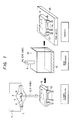
- the heat-treatment is carried out in an annealing furnace the atmosphere of which is filled by hot air or with an inert gas such as an N2 gas and which has a heat block 12 or the like.
- This annealing may be effected in a lamp annealing apparatus using a halogen lamp or an argon lamp.
- the relative humidity of the internal gas of the annealing furnace or the lamp annealing apparatus is such that a moisture reaches the chip 7 during annealing but aluminum wirings on the chip are not corroded by the entering moisture.
- the relative humidity is such that the defect of moisture-proofness of the chip 7 can be prevented.
- the relative humidity is preferably below from 40% to 50%, and more preferably from below 10% to 20%.
- the annealing cost can be reduced by carrying out the annealing step in air, it is preferably carried out in an inert gas such as the N2 gas (non-oxidizing atmosphere) in order to prevent oxidation of lead materials of IC.
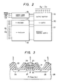
- the chip 7 described above has a system construction such as shown in Fig. 2, for example. Namely, it comprises of a 64 K bit memory matrix 21, an X decoder 18, a Y decoder 17, a Y gate 20, an output buffer 19, and a program logic control circuit 16 for controlling a disenable or enable state, or the like.
- Each memory cell as the memory means that constitutes the memory matrix has a known laminated gate memory cell structure using a metal oxide semiconductor field effect transistor (hereinafter called "MOSFET”) such as shown in Fig. 3.
- MOSFET metal oxide semiconductor field effect transistor
- the threshold voltage of N-MOSFET becomes extremely high and a so-called "low (L) state” is established where the channel is not formed even when a negative potential is applied to the gate electrode (G) 23.
- the memory cell is under the state where the channel is formed and a so-called “high (H)” state is established. Accordingly, the data can be stored.
- the electrons are injected by effecting annealing to cause thermal excitation so that the positive charge is neutralized or transferred by applying thereto the thermal energy. Data erasure for effecting stable re-writing can be made only after this step.
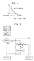
- V cc Assuming that the data are not completely erased and the electrons remain at the floating gate, a higher V cc is necessary for writing "H". In other words, when the completely erased memory cell and the incompletely erased memory cell are compared with other, "H" written by the same V cc is weaker in the incompletely erased memory cell and hence the access time becomes much more elongated.
- Fig. 4 shows this, relation between V cc and the access time
- Table 1 illustrates the result of judgement wherein V cc at the access time of 3,000 ns is called V ccmin A, and the memory cells whose V ccmin A is below 4.5 V are judged as accepted products having good erasing characteristics.
- Table 4 shows the result of judgement of the characteristics of the samples Nos. 1 to 5 to which the X-ray irradiation is made at 40 KV and 30 mA for 60 minutes using the Cr target and which are then subjected to annealing at 150°C for 24 hours. Since the X-ray irradiation energy (V2 ⁇ I ⁇ T) is too great, the X-ray damage is so great that the satisfactory writing characteristics cannot be obtained even when annealing is made.
- Table 5 shows the test results of the data retention characteristics by irradiating the X-rays to the samples at 30 KV and 40 mA for 15 minutes using the Cr target and by changing the annealing time while the annealing temperature is fixed at 170°C. It can be understood from this table that annealing must be made for at least 4 hours in order to obtain the satisfactory data retention characteristics.
- Table 6 shows the test results of the erasing characteristics of OTPROMs by irradiating the X-rays to the memory cells under the same condition as that of Table 5 and then changing the annealing time while the annealing temperature is fixed at 170°C. The satisfactory erasing characteristics can be obtained when annealing is made for 2 hours.
- the X-rays must satisfy the requirements, i.e. (1) they must have energy such that they can pass through the molding member and reach the chip, but (2) they have an optimal energy value so that they do not impart excessive damage to the chip.
- the X-rays consist of continuous X-rays and characteristics X-rays. The shorter the wavelength, the higher becomes the material transmission effect of the X-rays and the greater becomes the X-ray damage of the member to which the X-rays are irradiated. On the other hand, the longer the wavelength, the lower the transmission effect, so that the X-rays will be absorbed by the resin package and the like and cannot sufficiently reach the chip.
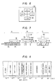
- Fig. 8 shows the classification of electromagnetic waves in accordance with their wavelengths.
- the X-rays to be used are preferably in the range of soft X-rays.
- the wavelengths K ⁇ 1 and K ⁇ 2 of the characteristics X-rays of Cr used for the experiments described already are from 0.2 to 0.3 nm. If carbon C is used in place of the Cr target, for example, the wavelength of the resulting X-rays is so long that the X-rays are absorbed by the resin package and cannot sufficiently reach the chip.
- the wavelength K ⁇ 1 and K ⁇ 2 of the resulting characteristic X-rays are about 0,021 nm and are within the range of hard X-rays. Therefore, the wavelength of the X-rays is so short that damge to the memory chip (memory chip itself and its peripheral circuits) will be too great. Thus, the X-ray target must be selected carefully.
- sample examination if any samples are found defective in the sampling test (sample examination) after extraction of the samples, the products of that lot are subjected once to the write and read tests (lot inspection, lot examination, total inspection), and only those products which are surely judged as defective are discarded while the data of the rest of the products are erased in accordance with the present method and the products are then shipped.
- the present invention can be applied not only to OTPROM but also to single chip microcomputer with built-in PROMs.
- the single chip microcomputer comprises of CPU 41, RAM 42, I/0 port 43 and PROM 44 as shown in Fig. 6, and is molded by plastics or the like.
- the inventors of the present invention conducted the experiments by irradiating the X-rays to the single chip microcomputer and then annealing it.
- the experimental condition is the same as described already, and the experiment is effected so that the X-rays are concentrated on the PROM portion.
- the result is found to be extremely satisfactory in the same way as in the case of OTPROM.
- Table 7 shows examples of the results.
- Fig. 7 shows an example of such an apparatus.
- An automatic transfer machine using an air conveyor transfers ICs to a portion B, then brings a mask 36 into close contact with each IC and thereafter irradiates the X-rays to only the necessary portions of the IC.
- annealing treatment is carried out by utilizing a heat block 38 and a hot jet to recover the X-ray irradiation damage.
- data erasure of PROM can be made reliably for single chip microcomputers, and the like.
Landscapes
- Physics & Mathematics (AREA)
- Engineering & Computer Science (AREA)
- Health & Medical Sciences (AREA)
- Computer Vision & Pattern Recognition (AREA)
- Electromagnetism (AREA)
- Toxicology (AREA)
- General Engineering & Computer Science (AREA)
- General Physics & Mathematics (AREA)
- Read Only Memory (AREA)
- Non-Volatile Memory (AREA)
- Encapsulation Of And Coatings For Semiconductor Or Solid State Devices (AREA)
- Analysing Materials By The Use Of Radiation (AREA)
Applications Claiming Priority (2)
| Application Number | Priority Date | Filing Date | Title |
|---|---|---|---|
| JP174152/85 | 1985-08-09 | ||
| JP60174152A JPS6235674A (ja) | 1985-08-09 | 1985-08-09 | 記憶装置のデ−タ消去方法 |
Publications (2)
| Publication Number | Publication Date |
|---|---|
| EP0212520A2 true EP0212520A2 (de) | 1987-03-04 |
| EP0212520A3 EP0212520A3 (de) | 1988-11-30 |
Family
ID=15973588
Family Applications (1)
| Application Number | Title | Priority Date | Filing Date |
|---|---|---|---|
| EP86111057A Withdrawn EP0212520A3 (de) | 1985-08-09 | 1986-08-08 | Datenverarbeitungsverfahren |
Country Status (4)
| Country | Link |
|---|---|
| EP (1) | EP0212520A3 (de) |
| JP (1) | JPS6235674A (de) |
| KR (1) | KR870002651A (de) |
| CN (1) | CN86105632A (de) |
Cited By (4)
| Publication number | Priority date | Publication date | Assignee | Title |
|---|---|---|---|---|
| US5656521A (en) * | 1995-01-12 | 1997-08-12 | Advanced Micro Devices, Inc. | Method of erasing UPROM transistors |
| EP1411526A3 (de) * | 1998-07-17 | 2007-03-07 | Koninklijke Philips Electronics N.V. | Verfahren zum Löschen eines nichtflüchtigen Speichers |
| WO2015007847A1 (de) * | 2013-07-19 | 2015-01-22 | Fraunhofer-Gesellschaft zur Förderung der angewandten Forschung e.V. | Verfahren zum löschen eines nicht flüchtigen halbleiterspeichers mit ionisierender strahlung |
| US20240211164A1 (en) * | 2022-12-27 | 2024-06-27 | Lionel UZZAN | Automated data erasure device and method |
Families Citing this family (2)
| Publication number | Priority date | Publication date | Assignee | Title |
|---|---|---|---|---|
| JPS63229696A (ja) * | 1987-03-18 | 1988-09-26 | Nec Corp | 読み出し専用メモリを有する半導体装置 |
| US6913649B2 (en) * | 2003-06-23 | 2005-07-05 | Sharp Laboratories Of America, Inc. | System and method for forming single-crystal domains using crystal seeds |
Family Cites Families (2)
| Publication number | Priority date | Publication date | Assignee | Title |
|---|---|---|---|---|
| JPS5330838A (en) * | 1976-09-03 | 1978-03-23 | Fujitsu Ltd | Erasing method of erasable rom |
| US4393479A (en) * | 1980-11-17 | 1983-07-12 | Texas Instruments Incorporated | Method for erasing data of a non-volatile semiconductor memory integrated circuit |
-
1985
- 1985-08-09 JP JP60174152A patent/JPS6235674A/ja active Pending
-
1986
- 1986-08-04 KR KR1019860006414A patent/KR870002651A/ko not_active Withdrawn
- 1986-08-08 EP EP86111057A patent/EP0212520A3/de not_active Withdrawn
- 1986-08-09 CN CN198686105632A patent/CN86105632A/zh active Pending
Cited By (5)
| Publication number | Priority date | Publication date | Assignee | Title |
|---|---|---|---|---|
| US5656521A (en) * | 1995-01-12 | 1997-08-12 | Advanced Micro Devices, Inc. | Method of erasing UPROM transistors |
| EP1411526A3 (de) * | 1998-07-17 | 2007-03-07 | Koninklijke Philips Electronics N.V. | Verfahren zum Löschen eines nichtflüchtigen Speichers |
| WO2015007847A1 (de) * | 2013-07-19 | 2015-01-22 | Fraunhofer-Gesellschaft zur Förderung der angewandten Forschung e.V. | Verfahren zum löschen eines nicht flüchtigen halbleiterspeichers mit ionisierender strahlung |
| US9633739B2 (en) | 2013-07-19 | 2017-04-25 | Fraunhofer-Gesellschaft Zur Foerderung Der Angewandten Forschung E.V. | Method of erasing information and device for performing same |
| US20240211164A1 (en) * | 2022-12-27 | 2024-06-27 | Lionel UZZAN | Automated data erasure device and method |
Also Published As
| Publication number | Publication date |
|---|---|
| JPS6235674A (ja) | 1987-02-16 |
| EP0212520A3 (de) | 1988-11-30 |
| KR870002651A (ko) | 1987-04-06 |
| CN86105632A (zh) | 1987-04-22 |
Similar Documents
| Publication | Publication Date | Title |
|---|---|---|
| US6246606B1 (en) | Memory using insulator traps | |
| KR910008103B1 (ko) | 박막 산화물 퓨우즈 | |
| US6566699B2 (en) | Non-volatile electrically erasable and programmable semiconductor memory cell utilizing asymmetrical charge trapping | |
| KR100433994B1 (ko) | 비대칭전하트래핑을사용하는비활성반도체메모리셀 | |
| Masuoka et al. | A new flash E 2 PROM cell using triple polysilicon technology | |
| EP0247875A2 (de) | Blockmässig elektrisch löschbarer Speicher | |
| JP3061924B2 (ja) | 不揮発性記憶装置の消去方法 | |
| US6930928B2 (en) | Method of over-erase prevention in a non-volatile memory device and related structure | |
| EP0108650A2 (de) | Programmierbarer MOS-Transistor | |
| EP0212520A2 (de) | Datenverarbeitungsverfahren | |
| US4590503A (en) | Electrically erasable programmable read only memory | |
| KR100506978B1 (ko) | 휘발성 반도체 메모리의 제조공정에서 제조된 불휘발성메모리 셀 트랜지스터를 퓨즈소자로서 갖는 반도체 집적회로장치 | |
| US4393479A (en) | Method for erasing data of a non-volatile semiconductor memory integrated circuit | |
| US5656521A (en) | Method of erasing UPROM transistors | |
| US6054351A (en) | Method of evaluating a tunnel insulating film | |
| US6842381B2 (en) | Method of marginal erasure for the testing of flash memories | |
| Sikora et al. | Technologies and reliability of modern embedded flash cells | |
| JP2907225B2 (ja) | 半導体記憶装置の製造方法 | |
| US7826287B2 (en) | Testing non-volatile memory devices for charge leakage | |
| US6822259B1 (en) | Method of detecting and distinguishing stack gate edge defects at the source or drain junction | |
| US7679150B2 (en) | Semiconductor device and programming method therefor | |
| US20040027877A1 (en) | Method for setting the threshold voltage of a field-effect transistor, field-effect transistor and integrated circuit | |
| JPH0534838B2 (de) | ||
| JPH01105397A (ja) | 記憶装置のデータ消去方法 | |
| Verma et al. | Proposed on-chip test structure to quantify trap densities within flash meories |
Legal Events
| Date | Code | Title | Description |
|---|---|---|---|
| PUAI | Public reference made under article 153(3) epc to a published international application that has entered the european phase |
Free format text: ORIGINAL CODE: 0009012 |
|
| AK | Designated contracting states |
Kind code of ref document: A2 Designated state(s): DE FR GB IT |
|
| PUAL | Search report despatched |
Free format text: ORIGINAL CODE: 0009013 |
|
| AK | Designated contracting states |
Kind code of ref document: A3 Designated state(s): DE FR GB IT |
|
| STAA | Information on the status of an ep patent application or granted ep patent |
Free format text: STATUS: THE APPLICATION IS DEEMED TO BE WITHDRAWN |
|
| 18D | Application deemed to be withdrawn |
Effective date: 19890627 |
|
| RIN1 | Information on inventor provided before grant (corrected) |
Inventor name: TOKAI, TATSUO Inventor name: ABE, AKIRA Inventor name: MITSUISHI, TOMOKUNI Inventor name: TAKEI, ICHIRO |