EP0214465B1 - Procédé de placage pour un élément électronique - Google Patents
Procédé de placage pour un élément électronique Download PDFInfo
- Publication number
- EP0214465B1 EP0214465B1 EP86110808A EP86110808A EP0214465B1 EP 0214465 B1 EP0214465 B1 EP 0214465B1 EP 86110808 A EP86110808 A EP 86110808A EP 86110808 A EP86110808 A EP 86110808A EP 0214465 B1 EP0214465 B1 EP 0214465B1
- Authority
- EP
- European Patent Office
- Prior art keywords
- plating
- electronic part
- pellet
- pad
- plating process
- Prior art date
- Legal status (The legal status is an assumption and is not a legal conclusion. Google has not performed a legal analysis and makes no representation as to the accuracy of the status listed.)
- Expired
Links
Images
Classifications
-
- C—CHEMISTRY; METALLURGY
- C25—ELECTROLYTIC OR ELECTROPHORETIC PROCESSES; APPARATUS THEREFOR
- C25D—PROCESSES FOR THE ELECTROLYTIC OR ELECTROPHORETIC PRODUCTION OF COATINGS; ELECTROFORMING; APPARATUS THEREFOR
- C25D5/00—Electroplating characterised by the process; Pretreatment or after-treatment of workpieces
-
- C—CHEMISTRY; METALLURGY
- C25—ELECTROLYTIC OR ELECTROPHORETIC PROCESSES; APPARATUS THEREFOR
- C25D—PROCESSES FOR THE ELECTROLYTIC OR ELECTROPHORETIC PRODUCTION OF COATINGS; ELECTROFORMING; APPARATUS THEREFOR
- C25D5/00—Electroplating characterised by the process; Pretreatment or after-treatment of workpieces
- C25D5/48—After-treatment of electroplated surfaces
- C25D5/50—After-treatment of electroplated surfaces by heat-treatment
-
- C—CHEMISTRY; METALLURGY
- C25—ELECTROLYTIC OR ELECTROPHORETIC PROCESSES; APPARATUS THEREFOR
- C25D—PROCESSES FOR THE ELECTROLYTIC OR ELECTROPHORETIC PRODUCTION OF COATINGS; ELECTROFORMING; APPARATUS THEREFOR
- C25D5/00—Electroplating characterised by the process; Pretreatment or after-treatment of workpieces
- C25D5/10—Electroplating with more than one layer of the same or of different metals
- C25D5/12—Electroplating with more than one layer of the same or of different metals at least one layer being of nickel or chromium
-
- C—CHEMISTRY; METALLURGY
- C25—ELECTROLYTIC OR ELECTROPHORETIC PROCESSES; APPARATUS THEREFOR
- C25D—PROCESSES FOR THE ELECTROLYTIC OR ELECTROPHORETIC PRODUCTION OF COATINGS; ELECTROFORMING; APPARATUS THEREFOR
- C25D5/00—Electroplating characterised by the process; Pretreatment or after-treatment of workpieces
- C25D5/60—Electroplating characterised by the structure or texture of the layers
- C25D5/615—Microstructure of the layers, e.g. mixed structure
- C25D5/617—Crystalline layers
-
- H—ELECTRICITY
- H10—SEMICONDUCTOR DEVICES; ELECTRIC SOLID-STATE DEVICES NOT OTHERWISE PROVIDED FOR
- H10W—GENERIC PACKAGES, INTERCONNECTIONS, CONNECTORS OR OTHER CONSTRUCTIONAL DETAILS OF DEVICES COVERED BY CLASS H10
- H10W70/00—Package substrates; Interposers; Redistribution layers [RDL]
- H10W70/01—Manufacture or treatment
- H10W70/04—Manufacture or treatment of leadframes
-
- H—ELECTRICITY
- H10—SEMICONDUCTOR DEVICES; ELECTRIC SOLID-STATE DEVICES NOT OTHERWISE PROVIDED FOR
- H10W—GENERIC PACKAGES, INTERCONNECTIONS, CONNECTORS OR OTHER CONSTRUCTIONAL DETAILS OF DEVICES COVERED BY CLASS H10
- H10W70/00—Package substrates; Interposers; Redistribution layers [RDL]
- H10W70/40—Leadframes
- H10W70/456—Materials
- H10W70/457—Materials of metallic layers on leadframes
-
- H—ELECTRICITY
- H05—ELECTRIC TECHNIQUES NOT OTHERWISE PROVIDED FOR
- H05K—PRINTED CIRCUITS; CASINGS OR CONSTRUCTIONAL DETAILS OF ELECTRIC APPARATUS; MANUFACTURE OF ASSEMBLAGES OF ELECTRICAL COMPONENTS
- H05K1/00—Printed circuits
- H05K1/02—Details
- H05K1/09—Use of materials for the conductive, e.g. metallic pattern
- H05K1/092—Dispersed materials, e.g. conductive pastes or inks
-
- H—ELECTRICITY
- H05—ELECTRIC TECHNIQUES NOT OTHERWISE PROVIDED FOR
- H05K—PRINTED CIRCUITS; CASINGS OR CONSTRUCTIONAL DETAILS OF ELECTRIC APPARATUS; MANUFACTURE OF ASSEMBLAGES OF ELECTRICAL COMPONENTS
- H05K3/00—Apparatus or processes for manufacturing printed circuits
- H05K3/22—Secondary treatment of printed circuits
- H05K3/24—Reinforcing of the conductive pattern
- H05K3/245—Reinforcing conductive patterns made by printing techniques or by other techniques for applying conductive pastes, inks or powders; Reinforcing other conductive patterns by such techniques
-
- H—ELECTRICITY
- H10—SEMICONDUCTOR DEVICES; ELECTRIC SOLID-STATE DEVICES NOT OTHERWISE PROVIDED FOR
- H10W—GENERIC PACKAGES, INTERCONNECTIONS, CONNECTORS OR OTHER CONSTRUCTIONAL DETAILS OF DEVICES COVERED BY CLASS H10
- H10W72/00—Interconnections or connectors in packages
- H10W72/071—Connecting or disconnecting
- H10W72/075—Connecting or disconnecting of bond wires
-
- H—ELECTRICITY
- H10—SEMICONDUCTOR DEVICES; ELECTRIC SOLID-STATE DEVICES NOT OTHERWISE PROVIDED FOR
- H10W—GENERIC PACKAGES, INTERCONNECTIONS, CONNECTORS OR OTHER CONSTRUCTIONAL DETAILS OF DEVICES COVERED BY CLASS H10
- H10W72/00—Interconnections or connectors in packages
- H10W72/50—Bond wires
-
- H—ELECTRICITY
- H10—SEMICONDUCTOR DEVICES; ELECTRIC SOLID-STATE DEVICES NOT OTHERWISE PROVIDED FOR
- H10W—GENERIC PACKAGES, INTERCONNECTIONS, CONNECTORS OR OTHER CONSTRUCTIONAL DETAILS OF DEVICES COVERED BY CLASS H10
- H10W72/00—Interconnections or connectors in packages
- H10W72/90—Bond pads, in general
- H10W72/951—Materials of bond pads
- H10W72/952—Materials of bond pads comprising metals or metalloids, e.g. PbSn, Ag or Cu
-
- H—ELECTRICITY
- H10—SEMICONDUCTOR DEVICES; ELECTRIC SOLID-STATE DEVICES NOT OTHERWISE PROVIDED FOR
- H10W—GENERIC PACKAGES, INTERCONNECTIONS, CONNECTORS OR OTHER CONSTRUCTIONAL DETAILS OF DEVICES COVERED BY CLASS H10
- H10W90/00—Package configurations
- H10W90/701—Package configurations characterised by the relative positions of pads or connectors relative to package parts
- H10W90/751—Package configurations characterised by the relative positions of pads or connectors relative to package parts of bond wires
- H10W90/754—Package configurations characterised by the relative positions of pads or connectors relative to package parts of bond wires between a chip and a stacked insulating package substrate, interposer or RDL
Definitions
- the invention relates to an electronic part having gold-plating on its metallic surface.
- Gold is widely used in various electronic parts because of its excellent heat resistance, corrosion resistance, solderability, wire bonding property and pellet-bonding property owing to formation of Au-Si eutectic alloy.
- Ni-plating is applied to the pad, and leads are connected to the pad which require lead connecting by soldering. Then coatings by Ni-plating, Co-plating and further Au-plating are applied onto a conductor by electric plating in that order.
- semiconductor pellet is subjected to die-bonding the on pad. After the pellet is connected to other pad by a wire bonding process, the semiconductor is sealed by glass having a low melting point, or the like.
- Ni-Co plating as primer coating for Au-plating herein is applied to prevent problems which are caused by peeling of Au-plating during seal heating after wire bonding. But in the step of further Co-plating onto Ni-plated film, hydrogen gas produced during the plating is occluded into plated layers, and thus remains as voids in Au-Si alloy formed on pellet upon pellet-bonding by heating at the step of pellet-bonding and the sealing by a low melting point glass, and thus results in serious a defect regarding the reliability of the pellet-bonding. Moreover, Ni-Co-Au plated layer consists of three layers, and consequently strains in the plates between the layers is so large that the problem of peeling of the plated layers may arise when a lead is bent.
- the object of this invention is to provide a plating process for an electronic part which has no voids in Au-Si eutectic crystals formed upon pellet-bonding when Au-plating is applied as the primary coating on Ni-Co platings for an electronic part.
- the characteristic of the invention is the plating process of an electronic part that is annealed after Ni-plating, Co-plating and a further Au-plating have been applied onto its metallic surface in that order.
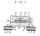
- Fig. 1 is the sectional view of an electronic part.
- Fig. 1 is the sectional view of a finished electronic part in which 1, 9, 10 and 5 are a ceramic board, a semiconductor pellet, a wire treated with wire bonding and a lead extended from this electronic part, respectively.
- 2a, 2b and 2c are conductor pads formed on ceramic board 1, i.e., a pad connected with pellet 9, a pad connected by a wire bonding and a pad connected with lead 5, respectively.
- 11 is a sealing cap. The method of the working example is explained below in due order.
- pads constituted of a metal having a high melting point such as W or Mo, etc. are formed on the ceramic substrate board 1 by a screen printing process, etc.
- the pads 2a, 2b and 2c are formed by consolidatedly mutual sintering of ceramic and the metal.
- Ni is plated on pads 2a, 2b and 2c to form Ni-plated film 3.
- pad 2c is soldered with lead 5 by a soldering material 4 such as eutectic silver.
- a soldering material 4 such as eutectic silver.
- Ni-plated film 6, Co-plated film 7, and further an Au-plated film 8 thereonto are formed in 2-5 pm, 0.5-2 pm, and 1-3 pm of thickness, respectively, by electric plating.
- the electronic part is annealed by heating up to 450°C, for 10 minutes under N 2 atmosphere.
- pellet 9 is die-bonded to pad 2a, and pellet 9 is connected to pad 2b through wire 10 by wire bonding, and a sealing cap 11 is fused to the ceramic board 1 with a low melting point glass to seal pellet 9, and finally lead 5 is coated with solder.
- This invention can give a reliable plating process for an electronic part, which yields no voids in Au-Si eutectic crystal because it can eliminate residual gases in a'plating by an annealing process after plating.
Landscapes
- Chemical & Material Sciences (AREA)
- Organic Chemistry (AREA)
- Chemical Kinetics & Catalysis (AREA)
- Electrochemistry (AREA)
- Materials Engineering (AREA)
- Metallurgy (AREA)
- Engineering & Computer Science (AREA)
- Crystallography & Structural Chemistry (AREA)
- Electroplating Methods And Accessories (AREA)
- Die Bonding (AREA)
- Other Surface Treatments For Metallic Materials (AREA)
- Wire Bonding (AREA)
- Electroplating And Plating Baths Therefor (AREA)
- Electric Connection Of Electric Components To Printed Circuits (AREA)
- Lead Frames For Integrated Circuits (AREA)
Claims (4)
Applications Claiming Priority (2)
| Application Number | Priority Date | Filing Date | Title |
|---|---|---|---|
| JP60195856A JPS6256597A (ja) | 1985-09-06 | 1985-09-06 | 電子部品のメツキ方法 |
| JP195856/85 | 1985-09-06 |
Publications (2)
| Publication Number | Publication Date |
|---|---|
| EP0214465A1 EP0214465A1 (fr) | 1987-03-18 |
| EP0214465B1 true EP0214465B1 (fr) | 1988-12-28 |
Family
ID=16348133
Family Applications (1)
| Application Number | Title | Priority Date | Filing Date |
|---|---|---|---|
| EP86110808A Expired EP0214465B1 (fr) | 1985-09-06 | 1986-08-05 | Procédé de placage pour un élément électronique |
Country Status (5)
| Country | Link |
|---|---|
| US (1) | US4765528A (fr) |
| EP (1) | EP0214465B1 (fr) |
| JP (1) | JPS6256597A (fr) |
| KR (1) | KR900003472B1 (fr) |
| DE (1) | DE3661547D1 (fr) |
Families Citing this family (5)
| Publication number | Priority date | Publication date | Assignee | Title |
|---|---|---|---|---|
| JPH0364494A (ja) * | 1989-07-31 | 1991-03-19 | Yazaki Corp | 金めっき被膜の処理方法 |
| KR960039315A (ko) * | 1995-04-06 | 1996-11-25 | 이대원 | 리드프레임 제조방법 |
| JP3890539B2 (ja) * | 1996-04-12 | 2007-03-07 | Dowaホールディングス株式会社 | セラミックス−金属複合回路基板 |
| KR100243368B1 (ko) * | 1996-10-18 | 2000-02-01 | 유무성 | 리드프레임의 열처리 방법 |
| CN102544884B (zh) * | 2011-12-23 | 2015-04-01 | 富士康(昆山)电脑接插件有限公司 | 电连接器、电连接器壳体及其表面处理的方法 |
Family Cites Families (5)
| Publication number | Priority date | Publication date | Assignee | Title |
|---|---|---|---|---|
| JPS5644794A (en) * | 1979-09-14 | 1981-04-24 | Toyota Motor Corp | Dehydrogenation treatment of plated member |
| US4411965A (en) * | 1980-10-31 | 1983-10-25 | Occidental Chemical Corporation | Process for high speed nickel and gold electroplate system and article having improved corrosion resistance |
| JPS58158950A (ja) * | 1982-03-16 | 1983-09-21 | Nec Corp | 半導体装置 |
| EP0127857B1 (fr) * | 1983-05-28 | 1987-07-29 | Masami Kobayashi | Objet soudable en acier inoxydable et procédé pour sa fabrication |
| JPS60115247A (ja) * | 1983-11-28 | 1985-06-21 | Fujitsu Ltd | 半導体装置 |
-
1985
- 1985-09-06 JP JP60195856A patent/JPS6256597A/ja active Pending
-
1986
- 1986-06-25 KR KR1019860005072A patent/KR900003472B1/ko not_active Expired
- 1986-08-05 EP EP86110808A patent/EP0214465B1/fr not_active Expired
- 1986-08-05 DE DE8686110808T patent/DE3661547D1/de not_active Expired
- 1986-08-12 US US06/895,842 patent/US4765528A/en not_active Expired - Fee Related
Non-Patent Citations (2)
| Title |
|---|
| PATENT ABSTRACT OF JAPAN, unexamined applications, C field, vol. 8, no. 46, 29.02.84. THE PATENT OFFICE JAPANESE GOVERNMENT page 65 C 212 * |
| PATENT ABSTRACT OF JAPAN, unexamined applications, C field, vol.4, no.69, 22.05.80. THE PATENT OFFICE JAPANESE GOVERNMENT page 66 C 11 * |
Also Published As
| Publication number | Publication date |
|---|---|
| JPS6256597A (ja) | 1987-03-12 |
| US4765528A (en) | 1988-08-23 |
| KR870003234A (ko) | 1987-04-16 |
| EP0214465A1 (fr) | 1987-03-18 |
| DE3661547D1 (en) | 1989-02-02 |
| KR900003472B1 (ko) | 1990-05-19 |
Similar Documents
| Publication | Publication Date | Title |
|---|---|---|
| US3729820A (en) | Method for manufacturing a package of a semiconductor element | |
| US3881884A (en) | Method for the formation of corrosion resistant electronic interconnections | |
| US4675243A (en) | Ceramic package for semiconductor devices | |
| JPS60257160A (ja) | 半導体装置 | |
| JPS6043851A (ja) | 被覆金属リ−ドフレ−ム基板 | |
| EP0537162A1 (fr) | Boitier electronique en metal possedant une resistance amelioree aux perturbations electromagnetiques | |
| USH498H (en) | Electronic component including soldered electrical leads | |
| EP0214465B1 (fr) | Procédé de placage pour un élément électronique | |
| US7329944B2 (en) | Leadframe for semiconductor device | |
| JPS61140160A (ja) | 半導体用リ−ドフレ−ム | |
| JPS6149450A (ja) | 半導体用リ−ドフレ−ム | |
| JP2627509B2 (ja) | 導電層を有する電子部品 | |
| JP2000068396A (ja) | ハーメチックシール用カバー | |
| Smith et al. | Hybrid Microcircuit Tape Chip Carrier Materials/Processing Trade-Offs | |
| JPS63137574A (ja) | メタライズ金属層の表面被覆構造 | |
| JPS6083356A (ja) | 半導体装置 | |
| JPS6214452A (ja) | 半導体用リ−ドフレ−ム | |
| JPS60195953A (ja) | 半導体装置およびその製造方法 | |
| JPS60107845A (ja) | 半導体用回路基板 | |
| JPS6178150A (ja) | 樹脂封止型半導体装置用リ−ドフレ−ム | |
| JPH07153866A (ja) | セラミック回路基板 | |
| JPS59144159A (ja) | プラスチツク封止型ic | |
| JPS60195952A (ja) | 半導体装置 | |
| JPS6273648A (ja) | 気密ガラス端子 | |
| JPS6383291A (ja) | 金の導電層を有する電子部品 |
Legal Events
| Date | Code | Title | Description |
|---|---|---|---|
| PUAI | Public reference made under article 153(3) epc to a published international application that has entered the european phase |
Free format text: ORIGINAL CODE: 0009012 |
|
| AK | Designated contracting states |
Kind code of ref document: A1 Designated state(s): DE FR GB |
|
| 17P | Request for examination filed |
Effective date: 19870320 |
|
| 17Q | First examination report despatched |
Effective date: 19880211 |
|
| GRAA | (expected) grant |
Free format text: ORIGINAL CODE: 0009210 |
|
| AK | Designated contracting states |
Kind code of ref document: B1 Designated state(s): DE FR GB |
|
| REF | Corresponds to: |
Ref document number: 3661547 Country of ref document: DE Date of ref document: 19890202 |
|
| ET | Fr: translation filed | ||
| PLBE | No opposition filed within time limit |
Free format text: ORIGINAL CODE: 0009261 |
|
| STAA | Information on the status of an ep patent application or granted ep patent |
Free format text: STATUS: NO OPPOSITION FILED WITHIN TIME LIMIT |
|
| 26N | No opposition filed | ||
| PGFP | Annual fee paid to national office [announced via postgrant information from national office to epo] |
Ref country code: FR Payment date: 19980616 Year of fee payment: 13 |
|
| PGFP | Annual fee paid to national office [announced via postgrant information from national office to epo] |
Ref country code: GB Payment date: 19980724 Year of fee payment: 13 |
|
| PGFP | Annual fee paid to national office [announced via postgrant information from national office to epo] |
Ref country code: DE Payment date: 19981029 Year of fee payment: 13 |
|
| PG25 | Lapsed in a contracting state [announced via postgrant information from national office to epo] |
Ref country code: GB Free format text: LAPSE BECAUSE OF NON-PAYMENT OF DUE FEES Effective date: 19990805 |
|
| GBPC | Gb: european patent ceased through non-payment of renewal fee |
Effective date: 19990805 |
|
| PG25 | Lapsed in a contracting state [announced via postgrant information from national office to epo] |
Ref country code: FR Free format text: LAPSE BECAUSE OF NON-PAYMENT OF DUE FEES Effective date: 20000428 |
|
| PG25 | Lapsed in a contracting state [announced via postgrant information from national office to epo] |
Ref country code: DE Free format text: LAPSE BECAUSE OF NON-PAYMENT OF DUE FEES Effective date: 20000601 |
|
| REG | Reference to a national code |
Ref country code: FR Ref legal event code: ST |