EP0216928A1 - Procede et appareil de compression de donnees video - Google Patents
Procede et appareil de compression de donnees video Download PDFInfo
- Publication number
- EP0216928A1 EP0216928A1 EP86900240A EP86900240A EP0216928A1 EP 0216928 A1 EP0216928 A1 EP 0216928A1 EP 86900240 A EP86900240 A EP 86900240A EP 86900240 A EP86900240 A EP 86900240A EP 0216928 A1 EP0216928 A1 EP 0216928A1
- Authority
- EP
- European Patent Office
- Prior art keywords
- image
- original image
- pixels
- data
- register
- Prior art date
- Legal status (The legal status is an assumption and is not a legal conclusion. Google has not performed a legal analysis and makes no representation as to the accuracy of the status listed.)
- Granted
Links
Images



Classifications
-
- G—PHYSICS
- G06—COMPUTING OR CALCULATING; COUNTING
- G06T—IMAGE DATA PROCESSING OR GENERATION, IN GENERAL
- G06T3/00—Geometric image transformations in the plane of the image
- G06T3/40—Scaling of whole images or parts thereof, e.g. expanding or contracting
-
- H—ELECTRICITY
- H04—ELECTRIC COMMUNICATION TECHNIQUE
- H04N—PICTORIAL COMMUNICATION, e.g. TELEVISION
- H04N1/00—Scanning, transmission or reproduction of documents or the like, e.g. facsimile transmission; Details thereof
- H04N1/387—Composing, repositioning or otherwise geometrically modifying originals
- H04N1/393—Enlarging or reducing
- H04N1/3935—Enlarging or reducing with modification of image resolution, i.e. determining the values of picture elements at new relative positions
Definitions
- the present invention relates to compression of image data, and, more particularly, to a method of and apparatus for compressing image data for use in displaying an image on a monitor or reproducing an image at a desired reproduction magnification based on image data obtained by photoelectrically scanning an original.
- color scanner It is well known in graphic arts to prepare color separation negatives or positives by applying predetermined processes to image data obtained by photoelectrically scanning an original by an image scanning and recording apparatus (hereinafter referred to as "color scanner").
- color scanner since desired color corrections or gradation changes are made in processing electric image signals, it is necessary to display an image to be processed on a monitor or to simulate the image on a desired layout, in order to e.g. in the case that an original image having loon pixels is to be compressed into an image having 350 pixels which correspond to the entire pixels of the monitor, it is possible to effect the compression in an approximate integer compression ratio like 1/3.
- an image displayed on the monitor is relatively small in comparison with an effective area of the monitor. This is undesirable in the graphic arts, because it is necessary to display an image as large as possible throughout the effective area of the monitor, especially in modern graphic arts which often requires quite fine and minute corrections and changes of the image.
- the aforementioned problems may be caused when a reduced image with a desired reduction ratio is reproduced from an original.
- Another object of the invention is to ensure an image to be displayed as large as possible on an effective area of a monitor.
- a further object of the invention is to simplify the hardware construction of the apparatus.
- an apparatus which comprises: compression data input means for inputting image compression data including both the number of pixels of an original image and the number of pixels of a desired compressed image; first processing means for assigning the pixels of the original image to the the same number of blocks as the pixels of the desired compressed image, based on said image compression data, which is adapted for the desired image compression; original image data storing means for storing the pixel data of the original image therein; and second processing mears for receiving the pixel data of the original image sequentially outputted from the original image data storing means and averaging the pixel data received theretofore every time respective pixel data are received, thereby outputting an average value of pixels forming respective blocks assigned by the first processing means.
- the apparatus further comprises third processing means having substantially the same construction as the first processing means; and fourth processing means having substantially the same construction as the second processing means.
- the first processing mears assigns the pixels of the original image sequentially aligned in the vertical direction to a predeterminec number of blocks.
- the second processing means averages the pixel data of respective blocks sequentially aligned in the vertical direction of the original image, in accordance with the assignment of blocks by the first processing means.
- the third processing means assigns the pixels of the original image sequentially aligned in the horizontal direction to a predetermined number of blocks.
- the fourth processing means averages the pixel data of respective blocks sequentially aligned in the horizontal direction of the original image, according to the assignment of blocks by the third processing means and based on the average value of respective blocks obtained by the second processing means.
- the first processing means preferably comprises: an adder to one of input terminals of which the number of pixel of a desired compressed image is inputted; a subtractor one of input terminals of which is connected to the output terminal of said adder; a first register connected to the output terminal of said subtractor, the output terminal of said first register being connected to the other input terminal of said adder so as to form a positive feedback, said first register latching an output from said subtractor thereinto synchronously with an input clock of the pixel data of the original image; a comparator one of the input terminals of which is connected to the output terminal of said first register, the number of pixels of the original image being inputted to the other terminal thereof; and a selector for selectively inputting either a zero signal or the number of pixels of the original image, the input terminal of said selector being connected to the output terminal of said comparator, the output terminal of said selector being in turn connected to the other input terminal of said subtractor.
- the comparator compares the output from the first register with the number of pixels of the original image. When the output of the first register is smaller than the number of pixels of the original image, the selector selects a zero signal, whereas when the output of the first register is larger than the number of pixels of the original image, said selector selects the number of pixels of the original image, and simultaneously the comparator outputs an assignment signal for assigning the predetermined number of pixels to a block.
- the second processing means preferably comprises: a second register for sequentially latching the pixel data of the original image thereinto synchronously with a clock signal; a subtractor, one of the input terminals of which is connected to the output terminal of said second register; a counter for counting said clock signal; divider means, one of the input terminals of which is connected to the output terminal of said subtractor, and the other input terminal of which is connected to said counter; an adder, one of the input terminals of which is connected to the output terminal of said divider means; a third register connected to the output terminal of said adder for latching the output of said adder synchronously with said clock signal, the output terminal of said third register being connected to the other output terminals of said adder and of said subtractor respectively; and a fourth register connected to the output terminal of said adder.
- the above mentioned divider means preferably comprises a ROM table and a multiplier.
- the counter is cleared by the assigment signal outputted from the first processing means, and the output from the adder is inputted to the fourth register synchronously with said assignment signal.
- Another feature of the present invention relates to method of compressing image data, which comprises the steps of: inputting image compression data including both the number of pixels of an original image and the number of pixels of a desired compressed image; assigning the pixels of the original image to the same number of blocks as that of pixels of said desired compressed image, based on said image compression data, which is adapted for this desired image compression; subsequentially inputting pixel data of the original image synchronously with an input clock signal; averaging the pixel data theretofore every time respective pixel data are inputted; and outputting the average value of pixel data at the time when the same number of the pixel data as that of pixel forming one block is inputted.
- the present invention produces practically useful advantages as follows: the image compression of an original image can be made at a desired compression ratio, and furthermore with high fdelity to the original image.
- image compression of an original image can be made at a desired compression ratio, and furthermore with high fdelity to the original image.
- image can be displayed as large as possible over the full effective area thereof, whereby a quite fine and minute image correction such as color correction can be easily made.
- image data compression is attained by a simple hardware arrangement.
- FIG. 1 is a block diagram schematically showing an outline of an image processing apparatus embodying the present invention, and described hereinafter is the color correction of an image by using this image precessing apparatus.
- An oricinal image is photoelectrically scanned by an image scanning apparatus (not shown) to obtain original image data, the image data being stored in an input disk (1) in the form of digital signals.
- the image data are read out sequentially from the input disk (1), which are compressed at a desired compression ratio by an image data compression circuit (8) provided to an interface (2).
- the image data are in turn stored in a first memory (4), through a data I/O register (3) according to the address assignment from an address generation circuit (9).
- the data compression by the circuit (8) is directed to conversion from the image of fine pixels stored in the input disk (1) to image data of relatively coarse pixels adapable for display on a monitor(6), which is described in detail later.
- the image data stored in the first memory (4) is then fed to a display control circuit (5) through the data I/0 register (3) to display an image to be processed on a color monitor (6).
- An operator can apply the color correction to the image by operating a tablet (17) and a keyboard (18), while observing the image displayed on the color monitor (6). That is, instructions from the tablet (17) and the keyboard (18) are delivered to a CPU (16) which produces masking data for masking an area to be corrected.
- the masking data are stored in a control memory (15), according to address assignment from the address generation circuit (9).
- the masking data are stored in the control memory (15) in such a manner that the inside of the contour is established as "1" while the outside as "0".
- the color correction for a desired portion is effected by an operation circuit (7) based on both the image data from the first memory (4) and the mask data from control memory (15).
- the image data from the first memory (4) are inputted from an input data line (24).
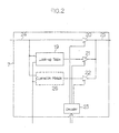
- ther image data for a part of the original image where color correction is not required are inputted, a buffer (20) is opened by a control code, through a decoder (23), given from the CPU (16) as an operation mode, and the image data are outputted to an output data line (25) by way of a pass-line.
- a buffer (21) is opened by a control code, through the decoder (23), provided by the CPU (16) as an operation mode, and the image data are corrected by a lookup table (19), which are outputted to the output data line (25).
- required correction data are supplied by the CPU (16) to the lookup table (19) according to the instruction by the operator, so that a desired color correction is applied to the image data inputted to the operation circuit (7).
- An operation module (26) is provided in the operation circuit (7) for other various operations, and the operation module (26) may be increased depending on the kind of operation required.
- the operation module (26) has various functions: such as color data processing, e.g. color masking correction, under color removal hue discrimination and gradation change; filtering processings, e.g. detail emphasizing; and masking processing, e.g. masking extraction.
- the hardware may be comprised of such components as operation elements for addition, subtraction, multiplication and division by using logical gates, comparator and I C devices having data processing function enabling pipe line procession, instead of the lookup table as mentioned above.
- the image data to which color correction has been applied by the operation circuit (7) are stored in a second memory (10) by way of a data 1/0 register (11) according to address assignment from the address generation circuit (9), and at the same time the content of correction in the operation circuit (7) is stored in a memory of the CPU (16) as historical data of the image correction applied to the image data stored in the first memory (4).
- An operator can confirm visually states of images prior and subsequent to the image correction by displaying alternately the image data stored in the first memory (4) prior to the correction and the image data stored in the second memory (10) after the correction on the color monitor (6).
- the image correction described above is applied to the image having coarse pixels stored in the first memory, i.e. to the image of which data is compressed by the data compression circuit (8), it is necessary to process the image data of fine pixels stored in the input disk (1) while referring to the historical data of the image correction stored in a memory provided in the CPU (16), and to store the corrected image which is confirmed by the operator on the color monitor (6), as image data of fine pixels which are adaptable for use in actual image reproduction, in an output disk (13).
- memeries (4), (10) and (15) are cleared by instructions from the keyboard (18), and the image data of fine pixels stored in the input disk (1) are stored in the first memory (4), by way of the interface (2) and the data I/O register (3), according to address assignment from the address generation circuit (9).
- it may be impossible to store all the image data of an image stored in the input disk (1) because the number of pixels obtained by scanning an original image of 10 cm square with a 50 ⁇ m sampling spot is up to 2000 x 2000 pixels, when each of the memories (4) (10) has an ordinary capacity of 1024 x 1024 pixels.
- the original image data are assigned to predetermined groups, and the image data of each of the groups are stored in the first memory (4) alternately.
- the image data stored in the first memory (4) are read out and inputted to the operation circuit (7), where a desired color correction is applied to the image data according to the historical data stored in the memory of the CPU (16).
- the image data are then stored in the second memory (10) according to address assignment from the address generation circuit (9) and further stored in the output disk (13) sequentially ir order by way of the data I/O register (11) and an interface (12).
- the corrected image data are stored in the output disk (13).
- the corrected image data are to be used as input data for an image recording apparatus (not shown), by which a reproduction image with desired color correction is obtained.
- FIG 3 is a circuit diagram which shows an embodiment of the image data compression circuit (8) according to the invention.
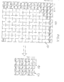
- the provision of the data compression circuit (8) is to compress the image data of fine pixels from the input disk (1) at a desired compression ratio as described above, but for the sake- of simplicity, described hereunder is a case of data compression in which image data of an original image comprising 12 x 15 pixels as shown in Figure 4(a) are compressed into the compressed image of 5 x 6 pixels as shown in Figure 4(b).
- a block (30) shown in Figure 3 is a circuit for applying DDA to the pixels aligned in the Y-direction of the original image (or) shown in Figure 4(a), in which the data compression in the Y-direction of the original image is carried out.
- the operator inputs desired compression data, i.e. a compression ratio of 5/12 in the X-direction and that of 6/15 in the Y-direction, to the CPU (16) through the keyboard (18).
- the CPU (16) in turn outputs a number signal (Yout) which represents the number of pixels in the Y-direction of the desired compression image (Co), i.e. "6", which is inputted to an adder (31) of the DDA circuit (30).
- the CPU (16) outputs a number signal (Yin) which represents the number of pixels aligned in the Y-direction of the original image (or), i.e. "15", which is inputted to a selector (32).
- a zero signal (“0") is inputted to another terminal of the selector (32).
- the number signal (Yout) from the CPU (16) is inputted to a register (34) by way of the adder (31) and a subtractor (33).
- the register (34) latches the number signal (Yout) synchronously with a clock signal (CY), and then outputs an accumulated value (SY) of the number signal (Yout), for positive feedback- to the other terminal of the adder (31).
- the output (SY) from the register (34) is further inputted to an input terminal of a comparator (35) for comparison with the number signal (Yin) inputted to the other input terminal of the comparator (35).
- the selector (35) When the value of the number signal (Yin) is bigger than that of the signal (SY), the selector (35) outputs a zero signal, which is inputted to the selector (32).
- the selector (32) At the time when the zero signal from the comparator (35) is inputted to the selector (32), the selector (32) outputs a zero signal to the subtractor (33). In such a way the number signal (Yout) is repeatedly latched into the register (34) synchronously with the clock signal (CY).
- the value of the output (SY) from the register (34) synchronously with the third clock signal (CY) results in "18".
- the value of the number signal (Yin) is smaller than that of the signal (SY), thus the comparator (35) outputs a "1" signal to the selector (32).
- the selector (32) outputs the number signal (Yin), i.e. "15", to the subtractor (33).
- the comparator (35) also generates a clock signal (CX) to clear a counter (41).
- the clock signal (CX) from the comparator (35) is counted by a counter (36) to be compared with the number signal (Yout) by a comparator (37). When the counted number reaches " Yout + 1", a signal (Yend) is outputted from the comparator (37).
- the counter (36) is cleared to be- "1" by the signal (Yend).
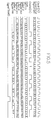
- the operations in the DDA circuit (30) described above are shown in the timing chart of Figure 5.
- the signal (CX) outputted from the DDA circuit (30) assigns a predetermined number of pixels aligned in the Y-direction with respect to the respective lines of the original image or), i.e. a 1.1, a 1.2, .... a 1.14, a 1.15; a 2.1, a 2.2 ..., a 2.14; a 2.15; a 12.1, ..., a 12.15, for respective pixels of the compressed image.
- pixel data (a x.y ) of the original image (Or) are sequentially inputted to an averaging circuit (40) provided in the image data comoression circuit (8) by way of the interface (2), and the pixel data (a x ⁇ y ) are latched into a register (-2) synchronously with the clock signal (CY) thereby outputting an image signal (a 1 ).
- the image signal (a 1 ) is inputted to a terminal of a subtractor (43), and an output (D 1 ) of the subtractor (43) is in turn inputted to a terminal of a multiplier (44).
- An inverse number of a counted value (i) is inputted from the counter (41) to the other terminal of the multiplier (44), by way of a ROM table (45).
- An output from the multiplier (44), i.e. Di/i, is inputted to a terminal of an adder (46), and an output (Mi) from the adder (46) is further inputted to a terminal of a register (47), where the output (Mi) of the adder (46) is latched thereinto synchronously with the clock signal (CY), and an output (M i-1 ) therefron is inputted to respective terminals of the adder (46) and the subtractor (43).
- the averaging circuit (40) has such an arrangement as described above, and subtractor (43) carries out the operation:
- M i-1 is the average value up to (i-l)the input data, and thus it can be expressed as follows:
- the function of the averaging circuit (40) in connection with, for example, the first line (a 1.1 -a 1.15 ) of the original image (OR) shown in Figure 4(a) is as follows.
- the pixel data (a x.y ) are latched into the register (42) in sequential order beginning with the pixel data (a 1.1 ) synchronously with the clock signal (CY), and every time the pixel data (a x.y ) ) are latched into the register (42), the average value (M i-1 ) of the pixel data latched theretofore is renewed.
- a difference (D3) between a value of the pixel (a 1.3 ) and an average value of both the pixels (a l . 1 ) and (a 1.2 ) - is outputted from the subtractor (43), which is inputted to a terminal of the multiplier (44).
- an inverse number of the number of the pixel signal (1) counted by the counter (41), i.e. the inverse number of "3” is inputted from the ROM table (45) to be multicliec in the multiplier (44).
- an output value of the is added to an average value up to the pixel (a 1.2 ) in the adder (46), and the output value (M 2 ) is into a register (48) syncnronessly with the clock signal (CX).
- the output value (M 3 ) latched is an average value of the pixels (a 1.1 ⁇ a 1 . a 1.3 ).
- both a value (a 5 ) of the pixel (a 1.5 ) and a value of the fourth pixel (the average value up to the third pixel is cleared by the clock signal (CX) are inputted to a terminal of the multiplier (44).
- an inverse number of the number of pixel signals (i), i.e. the inverse number of "2", counted by the counter (41) is inputted from the ROM table (45) to the other terminal of the multiplier (44) to be multiplied therein. Furthermore, an output value of the multiplier (44) is added to a value of the pixel (a 1.4 ) in the adder (46), and an output (M 5 ) therefrom is latched into the register (48) as an average value of the pixels (a 1.4 ) and (a 1.5 ) sanchronously with the clock signal (CX).
- the DDA circuit (30) it is decided to assign a predetermined number of pixels to compressed image pixels of a desired compression ratio, with respect to the pixels continuously aligned in the Y-direction of the original image (or), and the signal (CX) is outputted for asignment of the pixels.
- the assignment decided by the DDA circuit (30) for the first line shown in Figure 4 (a) results in six blocks, i.e.
- each average value of the pixel data for each block of the original image (Or) is also decided.
- the average value of the pixels (a 1.1 ⁇ a 1.3 ) of the original image (Or) is obtained from the register (48) as an output (b 1.1 ), that of the pixels (a 1,4 ⁇ a 1.5 ) as an output (bl.2) that of the pixels (a 1,6. ⁇ a 1.8 ) as an output (b 1.3 ), that of the pixels (a 1.9 ⁇ a 1.10 ) as an output (b 1.4 ), that of the pixels (a 1.11 ⁇ a 1.13 ) as an output (b l . 5 ) and that of the pixels ( a l.14 al.15) as an output (b 1.6 ), respectively.
- the data compression in the Y-direction is accomplished by both the DDA circuit (30) and the averaging circuit (40), while the data compression in the Y-direction is effected by both a DDA circuit (50) and an averaging circuit (60).
- the DDA circuit (50) is arranged substantially in the same manner as the DDA circuit (30), and in which the number of pixels aligned in the X-direction (Xout)-of the compressed image (Co), i.e. "5", is inputted to a terminal of an adder (51), while the number of pixels aligned in the X-direction (Xin) of the original (Or), i.e. "12", is Inputted to a terminal of a selector (52) respectively by instructions from the CPU (16).
- a clock signal applied to the resister (54) is an output of an AND gate (57), to which both the clock signal (CY) and the signal (Yend) are inputed.
- the register (54) outputs a signal (SX) synchroncusly with the clock signal outputted from the AND gate.
- SX Xin
- the comparator (55) outputs "1", by which the selector (52) outputs a number signal (Xin) which represents the number of pixels, i.e. "12".
- the output of the comparator (55) is inputted to a terminal of an AND gate (56), to the other terminal of which the signal (CX) is inputted, whereby a signal (CXY) is outputted from the AND gate (56).
- the output of the comparator (55) is further inputted to a counter (61) of the averaging circuit (60) to clear it.
- the signal (CXY) outputted from the DDA circuit (50) assigns the line pixels aligned in the X-direction of the original image (Or) shown in Figure 4(a) for a predetermined number adapted to the compressed image, that is, rescective blocks of 3 lines: 2 lines: 3 lines: 2 lines: 2 lines of the original (Or) correspond to each line of the compressed image.
- the average value for each block i.e. a 1.1 ⁇ a 1.3 .;a 1.4 ⁇ a 1.5 ; a 1.6 ⁇ a 1.8 ; a 1.9 ⁇ a 1.10 ; a 1.11 ⁇ a 1.13 ; a 1.14 ⁇ a 1.15 ; a 2.1 ⁇ a 2.3 ; a 2.4 ⁇ a 2.5 ..., determined by the DDA circuit (30) is latched into the register (48) synchronously with the clock signal (CX).
- the output (b x.y ) ) from the register (48) is inputted to a terminal of a subtractor (63), and an output from the subtractor (63) is further inputted to a terminal of a multiplier (64).
- To the other terminal of the multiplier (64) is inputted an inverse number of a counted value (j) from the counter (61) by way of a ROM table (65).
- An output from the multiplier (64) is inputted to a terminal of an adder (66), and an output from the adder (66) is further inputted to a terminal of a register (67) and to that of a selector (68) respectively.
- the selector (68) selects the input from the adder (66) when the input signal from the comparator (55) is zero, whereas it selects "0" when the input signal from the comparator (55) represents "1".
- a memory (69) a value counted by a counter (70) is written as a memory address, output from the selector (68). An output from the memory (69) is inputted to the other terminal of the adder (66) and to that of the subtractor (63) respectively.
- Average values of the pixel data for respective blocks (a 1.1 ⁇ a 1.3 ; a 1.4 ⁇ a 1.5 ; a 1.6 ⁇ a 1.8 ; a 1.9 ⁇ a 1.10 ; a 1.11 ⁇ a 1.13 ; a 1.14 ⁇ a 1.15 ) of the first line of the original image (Or) are latched into the register (48) synchronously with the clock signal (CX) in sequential order, and outputs (b 1.1 , b 1.2 , b 1.3 , b 1.4 , b 1.5 , b 1.6 ) are outputted from the register (48).
- the outputs (b 1.1 , b 1.2 , b 1.3 , b 1.4 , b 1.5 , bl.6) of the register (48) for the first line are written in the memory (69) as they are, according to the memory address given by the counter (70), since the value counted by the counter (61) represents "1" while the output of the memory (69) represents "0".
- the outputs are subtracted sequentially from outputs (N 1.1 , N 2.1 , N 3.1 , N 4.1 , N 5.1 , N 6.1 ) outputted from the memory (69) by the subtractor (63), and the results subtracted are sequentially inputted to the multiplier (69).
- the value counted by the counter (61) represents "2"
- the value 1/2 is inputted to the multiplier (64) by way of the ROM table (65) to effect the multiplication by 1/2.
- respective values of outputs (N 1.1 , N 2.1 , N 3.1 , N 4.1 , N 5.1 , N 6.1 ) outputted from the memory (69) are sequentially added to the respective resultant values of the multiplication.
- the results of the addition are stored sequentially in the memory (69) by way of the selector (68) according to address assicnment of the counter (70) to renew the contents stored in the memory (69).
- the data stored in the memory (69) are respective average values of the pixels (a 1.1 a 1.3 , a 2.1 a 2.3 , a 1.4 a 1.5 , a 2.4 a 2.5 , a 1.6 a 1.8 , a 2.6 a 2.8 , a 1.9 a 1.10 , a 2.9 a 2.10 , a 1.11 a 1.13 , a 2.11 a 2.13 , a 1.14 a 1.15 , a 2.14 a 2.15 ) of the original image (Or).
- the method and apparatus for compressing image data in accordance with the present invention is applicable when an original image is displayed on a monitor, or reproduced on a photosensitive material at a desired reduction ratio.
Landscapes
- Engineering & Computer Science (AREA)
- Physics & Mathematics (AREA)
- General Physics & Mathematics (AREA)
- Theoretical Computer Science (AREA)
- Multimedia (AREA)
- Signal Processing (AREA)
- Image Processing (AREA)
Abstract
Applications Claiming Priority (2)
| Application Number | Priority Date | Filing Date | Title |
|---|---|---|---|
| JP25874384 | 1984-12-06 | ||
| JP258743/84 | 1984-12-06 |
Publications (3)
| Publication Number | Publication Date |
|---|---|
| EP0216928A1 true EP0216928A1 (fr) | 1987-04-08 |
| EP0216928A4 EP0216928A4 (fr) | 1989-05-11 |
| EP0216928B1 EP0216928B1 (fr) | 1993-03-03 |
Family
ID=17324463
Family Applications (1)
| Application Number | Title | Priority Date | Filing Date |
|---|---|---|---|
| EP86900240A Expired - Lifetime EP0216928B1 (fr) | 1984-12-06 | 1985-12-06 | Procede et appareil de compression de donnees video |
Country Status (5)
| Country | Link |
|---|---|
| US (1) | US4764975A (fr) |
| EP (1) | EP0216928B1 (fr) |
| JP (1) | JP2583043B2 (fr) |
| DE (1) | DE3587155T2 (fr) |
| WO (1) | WO1986003610A1 (fr) |
Cited By (3)
| Publication number | Priority date | Publication date | Assignee | Title |
|---|---|---|---|---|
| FR2631766A1 (fr) * | 1988-05-17 | 1989-11-24 | Sony Corp | Procede et appareil de traitement d'un signal d'image fixe |
| WO1991013410A1 (fr) * | 1990-02-27 | 1991-09-05 | Eastman Kodak Company | Technique pour modifier numeriquement l'echelle d'une image en combinant ou en reproduisant logiquement les pixels dans des blocs de dimensions de groupe differentes |
| EP0521556A3 (en) * | 1991-07-05 | 1993-12-08 | Koninkl Philips Electronics Nv | Data processing system with means for display of reduced images and method for the reduction of images |
Families Citing this family (45)
| Publication number | Priority date | Publication date | Assignee | Title |
|---|---|---|---|---|
| IE852259L (en) * | 1985-09-13 | 1987-03-13 | Scottish & Newcastle Breweries | A method and apparatus for constructing, storing and¹displaying characters |
| US4947447A (en) * | 1986-04-24 | 1990-08-07 | Hitachi, Ltd. | Method for data coding |
| US5172245A (en) * | 1986-10-17 | 1992-12-15 | Sharp Kabushiki Kaisha | Electronic information retrieval apparatus for image information using primary and secondary menus |
| DE3852149T2 (de) * | 1987-06-19 | 1995-04-06 | Toshiba Kawasaki Kk | Kathodenstrahlröhre-/Plasmaanzeigesteuergerät. |
| EP0295689B1 (fr) * | 1987-06-19 | 1995-03-29 | Kabushiki Kaisha Toshiba | Dispositif de commande d'affichage pour une appareil de visualisation à TRC/plasma |
| US5351064A (en) * | 1987-06-19 | 1994-09-27 | Kabushiki Kaisha Toshiba | CRT/flat panel display control system |
| EP0295691B1 (fr) * | 1987-06-19 | 1994-11-23 | Kabushiki Kaisha Toshiba | Système de commutation du mode d'affichage pour un appareil de visualisation à plasma |
| EP0295690B1 (fr) * | 1987-06-19 | 1994-11-30 | Kabushiki Kaisha Toshiba | Système de commande de la zone de visualisation pour un dispositif d'affichage à plasma |
| GB2213345B (en) * | 1987-12-28 | 1992-01-15 | Mitsubishi Electric Corp | Image data filing system |
| JPH01233564A (ja) * | 1988-03-14 | 1989-09-19 | Fuji Photo Film Co Ltd | 放射線画像表示装置 |
| US5355447A (en) * | 1988-05-27 | 1994-10-11 | Wang Laboratories, Inc. | Method for color image reduction based upon determination of color components of pixels in neighboring blocks |
| US5161213A (en) * | 1988-05-27 | 1992-11-03 | Wang Laboratories, Inc. | Method for black and white image reduction based upon averaging black/white pixel counts of neighboring blocks |
| US5153936A (en) * | 1988-06-27 | 1992-10-06 | International Business Machines Corporation | Dual density digital image system |
| US5293485A (en) * | 1988-09-13 | 1994-03-08 | Kabushiki Kaisha Toshiba | Display control apparatus for converting color/monochromatic CRT gradation into flat panel display gradation |
| JP2909079B2 (ja) * | 1988-09-13 | 1999-06-23 | 株式会社東芝 | 表示制御方式 |
| EP0370323B1 (fr) * | 1988-11-23 | 1997-07-09 | Schlumberger Technologies, Inc. | Méthode et appareil de compression d'image haute résolution |
| US5086487A (en) * | 1988-11-24 | 1992-02-04 | Canon Kabushiki Kaisha | Method and apparatus for image encoding in which reference pixels for predictive encoding can be selected based on image size |
| US5250933A (en) * | 1989-03-02 | 1993-10-05 | Hewlett-Packard Company | Method and apparatus for the simultaneous display of one or more selected images |
| JPH0362090A (ja) * | 1989-07-31 | 1991-03-18 | Toshiba Corp | フラットパネル表示制御回路 |
| US5113455A (en) * | 1990-02-27 | 1992-05-12 | Eastman Kodak Company | Digital image scaling by stepwise pixel movement |
| US5022091A (en) * | 1990-02-28 | 1991-06-04 | Hughes Aircraft Company | Image processing technique |
| GB9006080D0 (en) * | 1990-03-17 | 1990-05-16 | Int Computers Ltd | Progressive encoding |
| CA2041819C (fr) * | 1990-05-07 | 1995-06-27 | Hiroki Zenda | Dispositif de commande d'afficheur couleur a cristaux liquides |
| US5070532A (en) * | 1990-09-26 | 1991-12-03 | Radius Inc. | Method for encoding color images |
| US5247589A (en) * | 1990-09-26 | 1993-09-21 | Radius Inc. | Method for encoding color images |
| JPH06318060A (ja) * | 1991-07-31 | 1994-11-15 | Toshiba Corp | 表示制御装置 |
| US5299028A (en) * | 1991-10-29 | 1994-03-29 | Eastman Kodak Company | Method and apparatus for image data resolution conversion |
| US5270695A (en) * | 1991-11-27 | 1993-12-14 | Eastman Kodak Company | Reduction technique for display of a radiographic image |
| FR2687034B1 (fr) * | 1992-02-04 | 1994-04-01 | Isaac Azancot | Procede et appareil de traitement-enregistrement et de reconstitution d'un signal video analogique haute resolution a cadence video normalisee destine aux procedures d'angiographie et d'angioplastie cardio vasculaire en temps reel. |
| JPH05244438A (ja) * | 1992-02-28 | 1993-09-21 | Canon Inc | 圧縮伸長回路 |
| US5400051A (en) * | 1992-11-12 | 1995-03-21 | International Business Machines Corporation | Method and system for generating variably scaled digital images |
| GB2273383A (en) * | 1992-12-10 | 1994-06-15 | Ibm | Character recognition |
| EP0610607A1 (fr) * | 1993-02-11 | 1994-08-17 | Agfa-Gevaert N.V. | Procédé pour l'évaluation du traitement d'image effectué sur une image radiographique |
| JPH06274612A (ja) * | 1993-03-17 | 1994-09-30 | Matsushita Electric Ind Co Ltd | 画像処理装置 |
| US5694149A (en) * | 1993-07-01 | 1997-12-02 | Intel Corporation | Vertically scaling image signals using digital differential accumulator processing |
| US5532717A (en) * | 1994-05-19 | 1996-07-02 | The United States Of America As Represented By The Secretary Of The Navy | Method of displaying time series data on finite resolution display device |
| US5745245A (en) * | 1995-01-06 | 1998-04-28 | Mita Industrial Co., Ltd. | Communication apparatus |
| GB9522077D0 (en) * | 1995-10-27 | 1996-01-03 | Univ Strathclyde | Data compression |
| US6094453A (en) * | 1996-10-11 | 2000-07-25 | Digital Accelerator Corporation | Digital data compression with quad-tree coding of header file |
| US6038033A (en) * | 1997-08-20 | 2000-03-14 | Lexmark International, Inc. | Method and apparatus for compressing and decompressing print data in the background operations of a printer |
| EP1042914A1 (fr) * | 1998-08-07 | 2000-10-11 | Koninklijke Philips Electronics N.V. | Compression adaptative |
| GB9817457D0 (en) * | 1998-08-12 | 1998-10-07 | Reckitt & Colman Inc | Improvements in or related to organic compositions |
| JP3937028B2 (ja) * | 1998-09-18 | 2007-06-27 | 富士フイルム株式会社 | 画像変換方法、画像変換装置及び画像変換プログラムを記録した記録媒体 |
| GB2354130B (en) * | 1999-09-09 | 2002-05-15 | Inventec Electronics | Method for enlarging/reducing digital images |
| KR102593265B1 (ko) * | 2019-04-08 | 2023-10-25 | 삼성전자주식회사 | 디스플레이 구동 장치 및 그 동작 방법 |
Family Cites Families (12)
| Publication number | Priority date | Publication date | Assignee | Title |
|---|---|---|---|---|
| GB1581546A (en) * | 1976-07-08 | 1980-12-17 | Xenotron Ltd | Compression and expansion of scanned images |
| GB1597484A (en) * | 1977-03-21 | 1981-09-09 | Rca Corp | Television picture compressor |
| GB2038142B (en) * | 1978-12-15 | 1982-11-24 | Ibm | Image data compression |
| JPS5676683A (en) * | 1979-11-28 | 1981-06-24 | Ricoh Co Ltd | Processing method for picture deformation |
| EP0051294B1 (fr) * | 1980-10-31 | 1986-10-01 | Kabushiki Kaisha Toshiba | Circuit de conversion de format d'image |
| US4541012A (en) * | 1982-01-04 | 1985-09-10 | Compression Labs, Inc. | Video bandwidth reduction system employing interframe block differencing and transform domain coding |
| DE3377447D1 (en) * | 1982-01-29 | 1988-08-25 | Toshiba Kk | Picture information display device |
| ATE16143T1 (de) * | 1982-05-28 | 1985-11-15 | Hell Rudolf Dr Ing Gmbh | Verfahren und einrichtung zur reproduktion eines bildes mit groeberer aufloesung als bei der bildabtastung. |
| US4528693A (en) * | 1982-09-30 | 1985-07-09 | International Business Machines Corporation | Apparatus and method for scaling facsimile image data |
| JPS59172686A (ja) * | 1983-03-23 | 1984-09-29 | フアナツク株式会社 | 画像表示方法 |
| GB2141607A (en) * | 1983-06-15 | 1984-12-19 | Philips Electronic Associated | Video display system with index pages |
| US4661987A (en) * | 1985-06-03 | 1987-04-28 | The United States Of America As Represented By The Secretary Of The Navy | Video processor |
-
1985
- 1985-12-06 WO PCT/JP1985/000671 patent/WO1986003610A1/fr not_active Ceased
- 1985-12-06 DE DE8686900240T patent/DE3587155T2/de not_active Expired - Fee Related
- 1985-12-06 EP EP86900240A patent/EP0216928B1/fr not_active Expired - Lifetime
- 1985-12-06 US US06/897,760 patent/US4764975A/en not_active Expired - Fee Related
- 1985-12-06 JP JP61500175A patent/JP2583043B2/ja not_active Expired - Lifetime
Cited By (3)
| Publication number | Priority date | Publication date | Assignee | Title |
|---|---|---|---|---|
| FR2631766A1 (fr) * | 1988-05-17 | 1989-11-24 | Sony Corp | Procede et appareil de traitement d'un signal d'image fixe |
| WO1991013410A1 (fr) * | 1990-02-27 | 1991-09-05 | Eastman Kodak Company | Technique pour modifier numeriquement l'echelle d'une image en combinant ou en reproduisant logiquement les pixels dans des blocs de dimensions de groupe differentes |
| EP0521556A3 (en) * | 1991-07-05 | 1993-12-08 | Koninkl Philips Electronics Nv | Data processing system with means for display of reduced images and method for the reduction of images |
Also Published As
| Publication number | Publication date |
|---|---|
| DE3587155D1 (de) | 1993-04-08 |
| JP2583043B2 (ja) | 1997-02-19 |
| EP0216928A4 (fr) | 1989-05-11 |
| US4764975A (en) | 1988-08-16 |
| WO1986003610A1 (fr) | 1986-06-19 |
| DE3587155T2 (de) | 1993-06-17 |
| EP0216928B1 (fr) | 1993-03-03 |
Similar Documents
| Publication | Publication Date | Title |
|---|---|---|
| EP0216928B1 (fr) | Procede et appareil de compression de donnees video | |
| EP0218633B1 (fr) | Procede et dispositif permettant de modifier des images numeriques en couleur | |
| EP0597555B1 (fr) | Appareil de traitement d'images | |
| EP0105116B1 (fr) | Amélioration des images vidéo par introduction sélective d'éléments d'image à échelle de gris | |
| EP0449407B1 (fr) | Appareils et méthodes pour le traitement de données, telles que les images en couleurs | |
| EP0227848A1 (fr) | Procédé pour le pré-traitement des images pour la suppression du bruit | |
| EP0269993B1 (fr) | Méthode et système de traitement d'image pour la reconstruction d'une image | |
| DE69032589T2 (de) | Farbbildverarbeitungsvorrichtung | |
| EP0442369B1 (fr) | Circuit de correction de gradation | |
| EP0264966B1 (fr) | Interpolateur pour système d'effets spéciaux de télévision | |
| JPS6255137B2 (fr) | ||
| EP0105085A2 (fr) | Procédé et appareil de filtrage de données d'image à échelle de gris | |
| US5489921A (en) | Method for generating uniform color area definitions with addition and removal operators | |
| US5140314A (en) | Image assembly | |
| US5559903A (en) | Method for generating geometric masks with a digital color computer | |
| US5502642A (en) | HSL neighborhoods in CMY color space | |
| JP2740517B2 (ja) | 画像処理装置 | |
| JPH07118002B2 (ja) | 画像処理装置 | |
| JP2844573B2 (ja) | 画像処理方法 | |
| JP2878477B2 (ja) | 画像処理装置 | |
| JPS61161891A (ja) | ビデオ製版装置における色修正方法 | |
| JP2737869B2 (ja) | 画像処理方法 | |
| JPH0721362A (ja) | ハイコントラスト処理装置 | |
| JPWO1986003610A1 (ja) | 画像データ圧縮装置 | |
| JPH0851509A (ja) | 画像処理装置 |
Legal Events
| Date | Code | Title | Description |
|---|---|---|---|
| PUAI | Public reference made under article 153(3) epc to a published international application that has entered the european phase |
Free format text: ORIGINAL CODE: 0009012 |
|
| 17P | Request for examination filed |
Effective date: 19860801 |
|
| AK | Designated contracting states |
Kind code of ref document: A1 Designated state(s): DE GB |
|
| A4 | Supplementary search report drawn up and despatched |
Effective date: 19890511 |
|
| 17Q | First examination report despatched |
Effective date: 19910524 |
|
| GRAA | (expected) grant |
Free format text: ORIGINAL CODE: 0009210 |
|
| AK | Designated contracting states |
Kind code of ref document: B1 Designated state(s): DE GB |
|
| REF | Corresponds to: |
Ref document number: 3587155 Country of ref document: DE Date of ref document: 19930408 |
|
| PLBE | No opposition filed within time limit |
Free format text: ORIGINAL CODE: 0009261 |
|
| 26N | No opposition filed | ||
| PGFP | Annual fee paid to national office [announced via postgrant information from national office to epo] |
Ref country code: GB Payment date: 19971127 Year of fee payment: 13 |
|
| PGFP | Annual fee paid to national office [announced via postgrant information from national office to epo] |
Ref country code: DE Payment date: 19971212 Year of fee payment: 13 |
|
| PG25 | Lapsed in a contracting state [announced via postgrant information from national office to epo] |
Ref country code: GB Free format text: LAPSE BECAUSE OF NON-PAYMENT OF DUE FEES Effective date: 19981206 |
|
| GBPC | Gb: european patent ceased through non-payment of renewal fee |
Effective date: 19981206 |
|
| PG25 | Lapsed in a contracting state [announced via postgrant information from national office to epo] |
Ref country code: DE Free format text: LAPSE BECAUSE OF NON-PAYMENT OF DUE FEES Effective date: 19991001 |