EP0220392A2 - In einer Rille angeordneter monolithischer Halbleiterkondensator und solche Kondensatoren enthaltende hochintegrierte dynamische Speicherzellen - Google Patents
In einer Rille angeordneter monolithischer Halbleiterkondensator und solche Kondensatoren enthaltende hochintegrierte dynamische Speicherzellen Download PDFInfo
- Publication number
- EP0220392A2 EP0220392A2 EP86110459A EP86110459A EP0220392A2 EP 0220392 A2 EP0220392 A2 EP 0220392A2 EP 86110459 A EP86110459 A EP 86110459A EP 86110459 A EP86110459 A EP 86110459A EP 0220392 A2 EP0220392 A2 EP 0220392A2
- Authority
- EP
- European Patent Office
- Prior art keywords
- capacitor
- layer
- polysilicon
- region
- mesa
- Prior art date
- Legal status (The legal status is an assumption and is not a legal conclusion. Google has not performed a legal analysis and makes no representation as to the accuracy of the status listed.)
- Granted
Links
Images


Classifications
-
- H—ELECTRICITY
- H10—SEMICONDUCTOR DEVICES; ELECTRIC SOLID-STATE DEVICES NOT OTHERWISE PROVIDED FOR
- H10B—ELECTRONIC MEMORY DEVICES
- H10B12/00—Dynamic random access memory [DRAM] devices
- H10B12/01—Manufacture or treatment
- H10B12/02—Manufacture or treatment for one transistor one-capacitor [1T-1C] memory cells
- H10B12/03—Making the capacitor or connections thereto
- H10B12/038—Making the capacitor or connections thereto the capacitor being in a trench in the substrate
-
- H—ELECTRICITY
- H10—SEMICONDUCTOR DEVICES; ELECTRIC SOLID-STATE DEVICES NOT OTHERWISE PROVIDED FOR
- H10B—ELECTRONIC MEMORY DEVICES
- H10B12/00—Dynamic random access memory [DRAM] devices
- H10B12/10—DRAM devices comprising bipolar components
-
- H—ELECTRICITY
- H10—SEMICONDUCTOR DEVICES; ELECTRIC SOLID-STATE DEVICES NOT OTHERWISE PROVIDED FOR
- H10B—ELECTRONIC MEMORY DEVICES
- H10B12/00—Dynamic random access memory [DRAM] devices
- H10B12/30—DRAM devices comprising one-transistor - one-capacitor [1T-1C] memory cells
- H10B12/37—DRAM devices comprising one-transistor - one-capacitor [1T-1C] memory cells the capacitor being at least partially in a trench in the substrate
-
- H—ELECTRICITY
- H10—SEMICONDUCTOR DEVICES; ELECTRIC SOLID-STATE DEVICES NOT OTHERWISE PROVIDED FOR
- H10W—GENERIC PACKAGES, INTERCONNECTIONS, CONNECTORS OR OTHER CONSTRUCTIONAL DETAILS OF DEVICES COVERED BY CLASS H10
- H10W10/00—Isolation regions in semiconductor bodies between components of integrated devices
- H10W10/01—Manufacture or treatment
- H10W10/011—Manufacture or treatment of isolation regions comprising dielectric materials
-
- H—ELECTRICITY
- H10—SEMICONDUCTOR DEVICES; ELECTRIC SOLID-STATE DEVICES NOT OTHERWISE PROVIDED FOR
- H10W—GENERIC PACKAGES, INTERCONNECTIONS, CONNECTORS OR OTHER CONSTRUCTIONAL DETAILS OF DEVICES COVERED BY CLASS H10
- H10W10/00—Isolation regions in semiconductor bodies between components of integrated devices
- H10W10/10—Isolation regions comprising dielectric materials
Definitions
- the invention relates to semiconductor devices and more particularly to a high capacitance and low-leakage integrated trench capacitor structure and a method for fabricating the same.
- the method is fully compatible with the advanced semiconductor manufacturing technologies, such as dielectric-filled trench isolation techniques to fabricate high density single device memory cells.
- Dynamic random access memories have been under active investigation by semiconductor manufacturers. According to the recent developments in this technology, fabrication of high density dynamic memory chips typically requires two device elements per storage cell, an active device (either a bipolar transistor or field effect transistor) and a passive device (e.g., capacitor).
- an active device either a bipolar transistor or field effect transistor
- a passive device e.g., capacitor
- the capacitor element In order to meet the ever-demanding requirements of higher integration density and superior performance of these memory structures, it is imperative that the capacitor element possess characteristics (both physical and electrical) which are consistent with these requirements. Among the different parameters which determine these capacitor characteristics, two are of significant importance: the surface area of the capacitor (which not only determines the capacitance but also the number of cells to be integrated in one chip) and leakage currents (which directly impact the ability of the capacitor to store the charge during the time between refresh cycles).
- a dynamic memory must have very low PN junction leakage currents in its storage node, even at elevated temperatures, e.g. 100°C and at the same time should also have a large capacitance in the storage node.
- the storage capacitor for dynamic memory cells consisted of one of the three junctions (emitter-base junction, collector-base junction or collector-substrate junction) associated with a bipolar transistor or the drain-substrate junction associated with a field effect transistor (FET).
- the bipolar transistor situation more specifically in case of a typical NPN device, it is well known that the leakage of the base-emitter junction is 2-3 orders of magnitude higher than that of the collector-base junction. If the charges are stored in the base of a bipolar transistor, they tend to leak away very fast because of the combined leakage of the base-emitter and base-collector junctions. If the charges are stored in the emitter, they are still subject to the high leakage of the emitter-base junction. On the other hand, if the charges are stored in a floating collector it tends to have about three orders of magnitude less leakage than the two other junctions rendering the floating collector as the desirable charge storage medium.
- the Jaccodine et al. process requires a specifically tailored and controlled ion implantation or diffusion step to form the doped regions constituting the one plate of the capacitor. Such a process is unsuitable in a high volume production environment. Also, to prevent formation of parasitic channels in the mesa surface region between the source/drain and the capacitor plate, the patented device requires a channel stop positioned adjacent to the capacitor plate in the mesa surface region. The channel stop-forming step further detracts the process from a high volume and high yield production environment. Yet another drawback of the Jaccodine et al.
- the Jaccodine et al. structure must have polysilicon-filled trench isolation, it suffers from the disadvantage associated with polysilicon trench isolation such as generation of defects in the silicon due to thermal mismatch between the trench-fill material and the trench insulator liner and that between the trench liner and the silicon substrate.
- the capacitor of the present invention overcomes all the disadvantages of the prior art structures and, in particular, the various problems associated with integrating an active device and a capacitor in a very dense configuration to form high performance dynamic one device cell.
- the capacitor structure is of the polysilicon-oxide-silicon (POS) type and is formed on the sidewalls of a mesa-shaped silicon regions delineated and surrounded by an isolation trench formed in the silicon material.
- the mesa-shaped silicon material serves as the first plate of the capacitor.
- a thin dielectric layer formed on the vertical sidewalls of the mesa serves as the capacitor insulator and a thin conductive polysilicon layer formed directly over the capacitor insulator serves as the second plate of the capacitor.
- the thin polysilicon layer is wrapped around the outer peripheral surface of the mesa. Since the second plate of the capacitor is formed as a coating of the vertical sidewalls of the mesa it encompasses a large area.
- the thin polysilicon layer which acts as the second plate of the capacitor does not fill the trench, but merely wraps around the trench sidewalls.
- the trench itself is filled with a plastic, low temperature deposition material, such as polyimide for device isolation purposes.
- the silicon substrate is of a first type of conductivity (e.g., P-) which is covered with an epitaxial silicon layer of the opposite type (e.g., N-).
- the stud- or mesa-shaped locations of the substrate containing the capacitor are provided with a heavily doped buried layer (e.g., N+) which can also be used as a low resistance subcollector of a bipolar transistor located in the silicon stud/mesa.
- the trench is etched into the substrate penetrating to a desired depth.
- Integrating the POS capacitor into the sidewalls results in a large storage capacitor because the surface area of the plate is the product of the depth of the trench and the perimeter of the mesa. It is therefore, easy to adjust the capacitance value either by adjusting the top planar dimensions of the mesa, the depth of the trench or both of these parameters.
- this particular structure significantly reduces PN junction leakage currents.
- the mesa includes an active device, the presence of this capacitor results in little or no increase in the device area thereby obtaining a very dense integrated circuit structure.
- the active device which is formed in a mesa-shaped silicon region, is a bipolar NPN transistor.
- the silicon mesa is dielectrically isolated from other adjacent mesas by polyimide-filled deep trenches.
- Fig. 1 the basics of a vertical bipolar NPN transistor structure 10 which results from conventional processing steps is shown.
- the basic structure 10 is comprised of a p-doped silicon structure 11, having a buried N+ subcollector 12 and N- epitaxial layer 13 thereon.
- the latter includes the vertical NPN transistor comprised of a N+ reach through region 14, a p-type base region 15 and a N+ emitter region 16.
- the structure is passivated with a composite insulating layer of silicon dioxide 17 of typical thickness of about 300 nm and silicon nitride 18 of approximate thickness 170 nm.
- the silicon nitride layer usually acts as an oxidation barrier to protect the top surface during trench sidewall oxidation. Any other desired active and/or passive devices would have been already incorporated into the structure at this stage of the process.
- the buried N+ subcollector may be either a blanket layer or composed of discrete regions formed at desired locations of the chip, for example, at the location where a bipolar transistor or capacitor structure of the present invention is to be formed.
- the exposed silicon is reactively ion etched in an atmosphere containing SF6, Cl2 and He to form deep and narrow trenches 19 by etching through the N- epitaxial layer 13, the N+ subcollector 12 and into the P- substrate 11 to produce the structure shown in Fig. 2.
- the trenches define a mesa-shaped silicon region 20 where active and/or passive devices may be located. Trench formation may be accomplished also by other techniques such as those detailed in U.S. Patent No. 4,381,953 to Ho et al. and copending application Serial No. 566,693 filed December 29, 1983 entitled "Trench Etch Process for Dielectric Isolation", by Goth et al., both of which are assigned to the present assignee.
- the trenches 19 are typically about 6 microns deep, 2 microns wide and have near vertical (i.e., greater than 85° with respect to the horizontal) sidewalls.
- the design layout of the trenches 19 is such that it delineates a square-shaped central stud or mesa 20 (which contains above-mentioned NPN transistor) enclosed by trenches 19 (Fig. 2).
- a standard ion implantation is conducted and boron is introduced at the bottom of the trenches 19 to create channel stop.
- the function of a channel stop is to avoid leakage between collector 12 in one mesa and its counterpart collector in an adjacent mesa due to inversion of the P- substrate 11 after forming the silicon dioxide layer 21.
- the next sequence of process steps is the formation in the trenches 19 of the four-layer composite consisting of the silicon dioxide 21, polysilicon 22, silicon dioxide 23 and silicon nitride 24.
- a thin oxide layer 21 having a thickness of about 30-100 nm is thermally grown to coat the sidewalls and floor of trench 19.
- a doped polysilicon layer 22 is formed on the resulting structure.
- An exemplary process of forming polysilicon 22 is by low pressure chemical vapor deposition (LPCVD) at a temperature of about 620°C obtaining about 200 nm to 300 nm thick blanket layer.
- LPCVD low pressure chemical vapor deposition
- This layer is then doped, for example, with phosphorous atoms to a high phosphorous concentration of ⁇ about 5 ⁇ 1019 atoms/cm3 to increase t polysilicon conductivity and attain a low sheet resistivity of about 50-100 ohms/square.
- doped polysilicon may be directly deposited on the oxide layer 21.
- the top surface of the polysilicon layer 22 is oxidized to form a thin silicon dioxide layer 23 of a thickness of about 50-100 nm.
- a thin silicon nitride layer 24 of about 50-100 nm thickness is blanket deposited by chemical vapor deposition at a temperature of about 775°C.
- the nitride 23 serves as a passivating overcoat.
- oxide 21 is grown only in the trench regions and not on the surface of the mesa 20 (which is protected from oxidation by the nitride layer 18). Consequently, while a four-layer composite (oxide 21 - polysilicon 22 - oxide 23 - nitride 24) is formed in the trench sidewalls and floor, a three-layer composite (polysilicon 22 - oxide 23 - nitride 24) is formed on the surface of mesa 20 which previously has been coated with oxide 17 and nitride 18.
- the next process step is patterning of the composite layers.
- the pattern definition of this composite layer is preferably accomplished in a two-step lithographic process.
- a photoresist block out mask (not shown) is used to remove the silicon nitride layer 24 from all regions where capacitors are not desired.
- Layer 24 is isotropically etched to remove the nitride from the trench sidewalls as well as from the horizontal surface of the mesa.
- An organic underlay material such as polyimide (2.0-4.0 ⁇ m thick) is first applied (not shown) onto the nitride layer 24 by spin coating.
- An inorganic barrier layer, for example SiOx, with a thickness in the 100 to 300 nm range is subsequently deposited in a CVD plasma.
- Polyimide is preferred over photoresist because it fills trenches without voids, is optically transparent, therefore allowing precise mask alignment, and lastly is thermally stable during deposition of the barrier layer.
- This step is followed by the application of a conventional photoresist such AZ 1340J (a trade name of Shipley Company), by spin coating.
- the photoresist layer is exposed according to a desired pattern to ultraviolet light through a mask and subsequently developed, in a conventional manner.
- the block out photoresist layer is typically 0.7-1.5 ⁇ m thick to optimize exposed image quality. It is important in our particular embodiment that the opening in the block out mask be wider than the mesa as apparent from Fig.2.
- the capacitor contact is defined by employing a contact mask and the process using polyimide discussed above.
- the silicon nitride overcoat layer 24 is anisotropically etched at this process stage, selectively retaining the overcoat layer 24 only on the trench sidewalls where the trench capacitor is required and on a desired portion on the horizontal top surface of the mesa at the location of the subcollector region 14, to delineate the top surface contact of the capacitor.
- the underlying silicon dioxide layer 23 and the N+ polysilicon layer 22 are, in turn, isotropically etched using the remaining portions of the nitride overcoat layer as an etch mask.
- Typical etchants include buffered HF for oxide removal and a solution composed of CrO3, HF and H2O to etch the N+ polysilicon layer without significant attack of the overcoat nitride layer 24.
- the resulting structure is illustrated in Fig. 4. As a result of etching the polysilicon 22, the then silicon dioxide 19 corresponding to the bottom of the trenches will be exposed.
- the contact mask not only overlap the trench sidewall as required, but also extends a little further in the trench. This process aspect has not been represented in Fig. 4.
- the polysilicon layer 22 is wrapped around the periphery of the mesa as a relatively thin coating on the vertical sidewalls of the mesa, leaving the trenches 19 available for filling with a dielectric medium.
- a preferred material for filling the trenches 19 is a material that is conducive for deposition at a low temperature.
- An example of this class of materials is plastic, more specifically, polyimide. This clearly distinguishes the present invention over the prior art according to which, the trench is filled with polysilicon.
- the use on a thin polysilicon layer instead of a solid polysilicon bar is considered as a primary feature of the present invention. Also, as is clear from Fig.
- portion 22a of the polysilicon layer 22 contains a small extension or tab 22′a just above the subcollector region 14. Tab 22′a will serve as a capacitor contact as will become more apparent later.
- the conductive polysilicon layer is formed only on the vertical sidewalls of the mesa-shaped, dielectrically isolated region 20. This allows each trench capacitor to be connected where desired. However in certain applications such as one-device dynamic RAM memory cell, it is desirable to have one plate of each capacitor connected to a common node of potential, such as the ground. In these applications, the conductive polysilicon layer may be left intact on the floor of the trenches, thereby providing a continuous polysilicon coating on the sidewalls of all mesa shaped isolated regions where a capacitor structure is to be formed.
- Device passivation is completed with the deposition of a blanket silicon nitride layer 26 as shown in Fig. 6.
- This layer is deposited in a CVD at a low temperature (approximately 750-800°C) to a thickness of about 50-150 nm.
- This layer provides a mobile ion passivation barrier for devices not provided with a capacitor structure.
- the next step is forming all device contacts including those at the bottom of all trench regions. This typically comprises to providing contact openings in correspondence with the silicon substrate regions that require either an ohmic or a rectifying contact. Openings are accomplished by CF4 reactive ion etch of the exposed portions of the silicon nitride layers 26 and 18 and followed by wet etching in 7:1 BHF of the exposed portions of oxide layers 21 and 17 as illustrated in Fig. 7.
- metal silicide contact metallurgy is then formed in all exposed silicon and polysilicon regions including all device contacts, polysilicon capacitor contacts, and the bottom of all trenches.
- a thin layer of an appropriate contact metal is blanket deposited on the whole structure by sputter deposition.
- a silicide forming metal selected from the group comprised of platinum, palladium, and the like, is used. The preferred metal is platinum with a layer thickness in the range of 20-100 nm.
- the structure is then heated at about 550°C to produce a platinum silicide layer wherever the platinum layer contacts silicon.
- the platinum silicide makes an ohmic contacts 25a, 29a, and 30a, respectively, with the N+ doped polysilicon capacitor contact 22a′, the highly doped N+ type collector reach-through 14 and emitter region 16.
- the platinum silicide also forms an ohmic contact 31a with the base region 15 and rectifying contact 27a to the thin N- inversion layer which exists at the bottom of the trenches 19. It will be appreciated that to form the rectifying contacts 27a the platinum metal must penetrate beyond the thickness of the inversion layer. Unreacted platinum is removed by wet etching (in aqua regia).
- pending application Serial No. 626,278 filed on June 29, 1984, entitled "Metal Silicide Channel Stoppers for Integrated Circuits and Method for Making the Same" by G. Goth et al.
- the processing at this point is substantially complete as far as the novelty of the invention is concerned.
- the balance of the processing is conventionally performed which includes filling of the trenches 19 with a dielectric material 19a such as polyimide by spin coating, baking at a suitable temperature to cure the polyimide and etching the unwanted polyimide by RIE using oxygen gas and standard personalization processing including metallization and passivation.
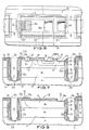
- FIG. 8 represents a top view of the structure depicted in Fig. 7.
- the capacitor contact 22a′ overlaps the subcollector region 14 and both are electrically connected by designing a metal stud 32 to short the capacitor to the collector of the transistor.
- the polysilicon contact should overlap the base region.
- the metal stud 32 is partly disposed above the deep polyimide filled trench 19 as shown in Fig. 8. As is evident from that Fig. 8, the polysilicon layer 22a is fully “wrapped” around the silicon mesa 20. The remaining composite silicon dioxide/silicon nitride layer which isolates the polysilicon layer from the polyimide fill is designated by numeral 33.
- the word line 34 and the bit line 35 are, respectively, formed at the first and second levels of metallization.
- the area of the capacitor is equal to the product of the mesa perimeter and trench depth.
- Typical capacitor area for dynamic memory application would be in the range of about 100-300 ⁇ m2 yielding a capacitance in the range of about 0.1-1.0 pF for capacitor insulator thickness in the range of about 15-50 nm.
- Fig. 9 shows an embodiment of a discrete integrated capacitor structure 36 formed using the process described hereinabove.
- the capacitor structure 36 shown in Fig. 9 is comprised of a N+ buried subcollector 12 and a N+ reach through region 14.
- One capacitor contact (C1) is made to the polysilicon tab 22a′ via ohmic contact 25a and the other contact (C2) is an ohmic contact 29a with the N+ reach through region 14.
- Alternative discrete capacitor structure may be readily designed.
- the N+ reach through region 14 may be provided to occupy either a limited or entire portion of the epitaxial layer.
- the buried layer 12 and the reach through region 14 may be merged into a single doped region coming in abuttment in the trench sidewalls, directly facing the polysilicon wrapping 22a inside the mesa-shaped isolated region of semiconductor (not represented), and separated from the polysilicon 22a by the thin oxide layer 21 forming the insulator of the capacitor structure.
- the formation of such a single doped region may be accomplished by conventional dopant diffusion or ion implantation.
- Such a discrete capacitor structure may be advantageously used for such analog applications as boot strap capacitors and series capacitors. It is noted that although for most applications the base of the mesa is generally rectangular or square in shape, as shown in Fig. 8, other shapes may be designed as well. For example, if a high capacitance capacitors are desired, serpentine- or comb-like, circular, and the like, structures can be formed to significantly increase the perimeter of the mesa.
- FIGs. 10 and 11 show, respectively, the cross-sectional and top views, of a metal oxide field effect transistor (MOSFET) dynamic single device memory cell structure 37 having an FET (specifically, p-FET) integrated with a trench-incorporated capacitor manufactured in accordance with the present invention.
- MOSFET metal oxide field effect transistor
- the memory cell is produced using the basic process steps described hereinabove and just two additional masking steps.
- Figs. 10 and 11 identical references as those in, for example, used to identify like features.
- the source and drain regions referenced in Fig. 10 as 38 and 39, respectively, are formed in the counterpart of the process step used form the base 15 of the NPN transistor (Fig. 7).
- the FET channel region is formed by removing the field oxide (not shown) from the N- epi region 13 (Fig. 10) between the source 38 and drain 39 and regrowing a thin (approximately 20-50 nm) gate oxide 37a.
- the gate electrode 40 of the FET is formed by depositing an N+ doped polysilicon layer and patterning the polysilicon layer into electrode 40.
- the polysilicon gate 40 is then coated with a composite silicon dioxide-silicon nitride insulator layer prior to contact definition.
- Source 38, drain 39, and gate 40 are then defined using the P contact mask for the NPN base, SBD anodes and P resistors.
- Metal silicide ohmic contacts 38a, 39a and 40a, respectively, with the source 38, drain 39 and gate 40, are then established as explained above by sputter deposition and sintering.
- a connecting stud 41 (shown in Fig. 11) makes the necessary connection between contacts 22a′ and 38a.
- FIGs. 12 and 13 show, respectively, the cross-sectional and top views, of a FET dynamic single device memory cell structure 42 comprised of an N-type FET integrated with a trench-incorporated capacitor manufactured in accordance with the principles of the present invention.
- Patterned N+ buried regions (not represented) are present where subcollectors for NPN transistors are necessary.
- Trenches 19 are formed in a conventional manner, but P+ channel stop regions 45 are formed by p-type dopant diffusion into the bottom and sidewall portions of the trenches.
- the diffused channel stop 45 eliminates leakage between the source 38 located in one silicon mesa and the drain located in a neighboring mesa due to inversion of the P- epi layer following oxidation of the trench sidewall.
- an N+ buried region 46 is additionally formed in the trench, in direct abuttment with the trench sidewalls.
- Region 46 is an N+ diffusion which provides an extension of region 47 down the trench sidewall. This sidewall diffusion serves as one plate of the trench capacitor. Details of the process for defining the N+ diffusion 46 are contained in the aforementioned U.S. Serial No. 626,271.
- Region 46 is used as an electrode plate of the capacitor and comes in contact with the drain region 47 as shown in Fig. 12.
- the gate electrode and source are referenced in Fig. 12 by numerals 48 and 49, respectively.
- the metallurgical contacts with the drain, source and gate electrode are referenced by references 47a, 49a and 48a, respectively.
- Connecting stud 50 (Fig. 13) makes the necessary connection between contacts 22a′ and 49a.
- the trench-incorporated capacitor structure disclosed hereinabove is not only of a high capacitance (e.g., 0.1 pF or higher) due to its unique structure, but also the capacitor does not consume valuable chip real estate. Another advantage is that it may be integrated with a transistor without necessitating any additional area. Since the capacitor capacitance is the product of the trench depth and parameter of the mesa, not only high value capacitance may be obtained but also the capacitance value can be readily adjusted as desired. For example, for a mesa of a given planar dimension, the capacitance may be increased by going deeper into the silicon (for more active area).
- the trench capacitor permits abuttment of elements of active devices (e.g. the emitter of a bipolar device) fabricated in conjunction with the capacitor fabrication directly against the trench sidewalls. Such butted arrangement further enhances the integrated circuit device density.
- the trenches may be filled with any desired dielectric material (e.g. polysilicon, polyimide, silicon dioxide) which is compatible with the desired dielectric isolation of other devices on the chip.
- the polysilicon layer which serves as a first plate electrode for one trench capacitor is not connected to any other capacitor plate electrode or devices formed in adjacent mesa surfaces.
Landscapes
- Engineering & Computer Science (AREA)
- Manufacturing & Machinery (AREA)
- Semiconductor Integrated Circuits (AREA)
- Semiconductor Memories (AREA)
- Bipolar Integrated Circuits (AREA)
Applications Claiming Priority (2)
| Application Number | Priority Date | Filing Date | Title |
|---|---|---|---|
| US792996 | 1985-10-30 | ||
| US06/792,996 US4704368A (en) | 1985-10-30 | 1985-10-30 | Method of making trench-incorporated monolithic semiconductor capacitor and high density dynamic memory cells including the capacitor |
Publications (3)
| Publication Number | Publication Date |
|---|---|
| EP0220392A2 true EP0220392A2 (de) | 1987-05-06 |
| EP0220392A3 EP0220392A3 (en) | 1989-06-14 |
| EP0220392B1 EP0220392B1 (de) | 1993-05-05 |
Family
ID=25158761
Family Applications (1)
| Application Number | Title | Priority Date | Filing Date |
|---|---|---|---|
| EP86110459A Expired - Lifetime EP0220392B1 (de) | 1985-10-30 | 1986-07-29 | In einer Rille angeordneter monolithischer Halbleiterkondensator und solche Kondensatoren enthaltende hochintegrierte dynamische Speicherzellen |
Country Status (5)
| Country | Link |
|---|---|
| US (1) | US4704368A (de) |
| EP (1) | EP0220392B1 (de) |
| JP (1) | JPS62105467A (de) |
| CA (1) | CA1258124A (de) |
| DE (1) | DE3688388T2 (de) |
Cited By (3)
| Publication number | Priority date | Publication date | Assignee | Title |
|---|---|---|---|---|
| EP0315483A3 (en) * | 1987-11-06 | 1990-10-10 | Sharp Kabushiki Kaisha | Semiconductor memory |
| EP0410633A3 (en) * | 1989-07-28 | 1991-02-27 | American Telephone And Telegraph Company | Planar isolation technique for integrated circuits |
| US20220319909A1 (en) * | 2021-04-01 | 2022-10-06 | Nanya Technology Corporation | Method for manufacturing a semiconductor memory device |
Families Citing this family (55)
| Publication number | Priority date | Publication date | Assignee | Title |
|---|---|---|---|---|
| KR900000170B1 (ko) * | 1984-06-05 | 1990-01-23 | 가부시끼가이샤 도오시바 | 다이내믹형 메모리셀과 그 제조방법 |
| USRE33261E (en) * | 1984-07-03 | 1990-07-10 | Texas Instruments, Incorporated | Trench capacitor for high density dynamic RAM |
| US5208657A (en) * | 1984-08-31 | 1993-05-04 | Texas Instruments Incorporated | DRAM Cell with trench capacitor and vertical channel in substrate |
| US5225697A (en) * | 1984-09-27 | 1993-07-06 | Texas Instruments, Incorporated | dRAM cell and method |
| US4824793A (en) * | 1984-09-27 | 1989-04-25 | Texas Instruments Incorporated | Method of making DRAM cell with trench capacitor |
| US5102817A (en) * | 1985-03-21 | 1992-04-07 | Texas Instruments Incorporated | Vertical DRAM cell and method |
| US5164917A (en) * | 1985-06-26 | 1992-11-17 | Texas Instruments Incorporated | Vertical one-transistor DRAM with enhanced capacitance and process for fabricating |
| US4829017A (en) * | 1986-09-25 | 1989-05-09 | Texas Instruments Incorporated | Method for lubricating a high capacity dram cell |
| JPS63122261A (ja) * | 1986-11-12 | 1988-05-26 | Mitsubishi Electric Corp | 半導体装置の製造方法 |
| US4830978A (en) * | 1987-03-16 | 1989-05-16 | Texas Instruments Incorporated | Dram cell and method |
| JPH0620108B2 (ja) * | 1987-03-23 | 1994-03-16 | 三菱電機株式会社 | 半導体装置の製造方法 |
| JPS6439057A (en) * | 1987-08-04 | 1989-02-09 | Nec Corp | Semiconductor storage device |
| US5109259A (en) * | 1987-09-22 | 1992-04-28 | Texas Instruments Incorporated | Multiple DRAM cells in a trench |
| JPH0795582B2 (ja) * | 1987-11-17 | 1995-10-11 | 三菱電機株式会社 | 半導体装置の溝型キャパシタセルの製造方法 |
| US4876217A (en) * | 1988-03-24 | 1989-10-24 | Motorola Inc. | Method of forming semiconductor structure isolation regions |
| US5105245A (en) * | 1988-06-28 | 1992-04-14 | Texas Instruments Incorporated | Trench capacitor DRAM cell with diffused bit lines adjacent to a trench |
| US5225363A (en) * | 1988-06-28 | 1993-07-06 | Texas Instruments Incorporated | Trench capacitor DRAM cell and method of manufacture |
| JPH0817224B2 (ja) * | 1988-08-03 | 1996-02-21 | 株式会社東芝 | 半導体記憶装置の製造方法 |
| US5188971A (en) * | 1988-12-28 | 1993-02-23 | Synergy Semiconductor Corporation | Process for making a self-aligned bipolar sinker structure |
| US5240867A (en) * | 1989-02-09 | 1993-08-31 | Fujitsu Limited | Semiconductor integrated circuit having interconnection with improved design flexibility, and method of production |
| US5206182A (en) * | 1989-06-08 | 1993-04-27 | United Technologies Corporation | Trench isolation process |
| US5017506A (en) * | 1989-07-25 | 1991-05-21 | Texas Instruments Incorporated | Method for fabricating a trench DRAM |
| US5065273A (en) * | 1990-12-04 | 1991-11-12 | International Business Machines Corporation | High capacity DRAM trench capacitor and methods of fabricating same |
| US5399516A (en) * | 1992-03-12 | 1995-03-21 | International Business Machines Corporation | Method of making shadow RAM cell having a shallow trench EEPROM |
| US5286667A (en) * | 1992-08-11 | 1994-02-15 | Taiwan Semiconductor Manufacturing Company | Modified and robust self-aligning contact process |
| US5438009A (en) * | 1993-04-02 | 1995-08-01 | United Microelectronics Corporation | Method of fabrication of MOSFET device with buried bit line |
| US5455064A (en) * | 1993-11-12 | 1995-10-03 | Fujitsu Limited | Process for fabricating a substrate with thin film capacitor and insulating plug |
| US6090716A (en) * | 1996-12-17 | 2000-07-18 | Siliconix Incorporated | Method of fabricating a field effect transistor |
| SE513471C2 (sv) * | 1997-11-17 | 2000-09-18 | Ericsson Telefon Ab L M | Halvledarkomponent och tillverkningsförfarande för halvledarkomponent |
| JP4221859B2 (ja) * | 1999-02-12 | 2009-02-12 | 株式会社デンソー | 半導体装置の製造方法 |
| DE19961779A1 (de) * | 1999-12-21 | 2001-07-05 | Infineon Technologies Ag | Integrierte dynamische Speicherzelle mit geringer Ausbreitungsfläche und Verfahren zu deren Herstellung |
| DE10121131C1 (de) * | 2001-04-30 | 2002-12-19 | Infineon Technologies Ag | Datenspeicher |
| US6995412B2 (en) * | 2002-04-12 | 2006-02-07 | International Business Machines Corporation | Integrated circuit with capacitors having a fin structure |
| US6875653B2 (en) * | 2002-08-02 | 2005-04-05 | Promos Technologies Inc. | DRAM cell structure with buried surrounding capacitor and process for manufacturing the same |
| US7208789B2 (en) * | 2002-08-02 | 2007-04-24 | Promos Technologies, Inc. | DRAM cell structure with buried surrounding capacitor and process for manufacturing the same |
| US6818534B2 (en) * | 2002-08-19 | 2004-11-16 | Infineon Technologies Richmond, Lp | DRAM having improved leakage performance and method for making same |
| US6905941B2 (en) * | 2003-06-02 | 2005-06-14 | International Business Machines Corporation | Structure and method to fabricate ultra-thin Si channel devices |
| US20070045698A1 (en) * | 2005-08-31 | 2007-03-01 | International Business Machines Corporation | Semiconductor structures with body contacts and fabrication methods thereof |
| US20070045697A1 (en) * | 2005-08-31 | 2007-03-01 | International Business Machines Corporation | Body-contacted semiconductor structures and methods of fabricating such body-contacted semiconductor structures |
| US7982284B2 (en) * | 2006-06-28 | 2011-07-19 | Infineon Technologies Ag | Semiconductor component including an isolation structure and a contact to the substrate |
| DE102007009383A1 (de) * | 2007-02-20 | 2008-08-21 | Fraunhofer-Gesellschaft zur Förderung der angewandten Forschung e.V. | Halbleiteranordnung und Verfahren zu deren Herstellung |
| US7691734B2 (en) | 2007-03-01 | 2010-04-06 | International Business Machines Corporation | Deep trench based far subcollector reachthrough |
| JP2009277851A (ja) * | 2008-05-14 | 2009-11-26 | Nec Electronics Corp | 半導体装置、半導体装置の製造方法及びパワーアンプ素子 |
| JP5763775B2 (ja) | 2010-11-02 | 2015-08-12 | エンパイア テクノロジー ディベロップメント エルエルシー | 絶縁されたスルーシリコンバイアを備えた半導体構造 |
| US8502307B2 (en) * | 2010-11-24 | 2013-08-06 | Infineon Technologies Ag | Vertical power semiconductor carrier having laterally isolated circuit areas |
| EP2919272B1 (de) * | 2014-03-12 | 2020-05-27 | Nxp B.V. | Bipolare Transistorvorrichtung und Verfahren zur Herstellung |
| WO2017052471A1 (en) * | 2015-09-23 | 2017-03-30 | Nanyang Technological University | Semiconductor devices and methods of forming the same |
| US20180047807A1 (en) * | 2016-08-10 | 2018-02-15 | Globalfoundries Inc. | Deep trench capacitors with a diffusion pad |
| US10100537B1 (en) | 2017-06-20 | 2018-10-16 | Allen Engineering Corporation | Ventilated high capacity hydraulic riding trowel |
| KR102501554B1 (ko) * | 2020-10-08 | 2023-02-17 | 에트론 테크놀로지, 아이엔씨. | 누설 전류가 감소되고 온/오프 전류를 조정할 수 있는 트랜지스터 구조체 |
| US11837601B2 (en) | 2021-05-10 | 2023-12-05 | Sandisk Technologies Llc | Transistor circuits including fringeless transistors and method of making the same |
| WO2022240452A1 (en) * | 2021-05-10 | 2022-11-17 | Sandisk Technologies Llc | Transistor circuits including fringeless transistors and method of making the same |
| US12027520B2 (en) | 2021-05-10 | 2024-07-02 | Sandisk Technologies Llc | Transistor circuits including fringeless transistors and method of making the same |
| US12094944B2 (en) | 2021-05-10 | 2024-09-17 | Sandisk Technologies Llc | Transistor circuits including fringeless transistors and method of making the same |
| US12087813B2 (en) * | 2021-08-31 | 2024-09-10 | Texas Instruments Incorporated | Deep trench isolation with field oxide |
Family Cites Families (18)
| Publication number | Priority date | Publication date | Assignee | Title |
|---|---|---|---|---|
| US3387286A (en) * | 1967-07-14 | 1968-06-04 | Ibm | Field-effect transistor memory |
| US3876992A (en) * | 1972-11-01 | 1975-04-08 | Ibm | Bipolar transistor memory with capacitive storage |
| US4017885A (en) * | 1973-10-25 | 1977-04-12 | Texas Instruments Incorporated | Large value capacitor |
| US4225945A (en) * | 1976-01-12 | 1980-09-30 | Texas Instruments Incorporated | Random access MOS memory cell using double level polysilicon |
| JPS5824023B2 (ja) * | 1978-02-28 | 1983-05-18 | 超エル・エス・アイ技術研究組合 | 半導体装置 |
| JPS5681968A (en) * | 1979-12-07 | 1981-07-04 | Toshiba Corp | Manufacture of semiconductor device |
| US4381953A (en) * | 1980-03-24 | 1983-05-03 | International Business Machines Corporation | Polysilicon-base self-aligned bipolar transistor process |
| US4353086A (en) * | 1980-05-07 | 1982-10-05 | Bell Telephone Laboratories, Incorporated | Silicon integrated circuits |
| JPS57201067A (en) * | 1981-06-04 | 1982-12-09 | Nec Corp | Semiconductor memory cell |
| JPS58154256A (ja) * | 1982-03-10 | 1983-09-13 | Hitachi Ltd | 半導体装置 |
| JPH0666436B2 (ja) * | 1983-04-15 | 1994-08-24 | 株式会社日立製作所 | 半導体集積回路装置 |
| JPS6058662A (ja) * | 1983-09-12 | 1985-04-04 | Nec Corp | 電荷一時蓄積記憶装置 |
| JPS60117658A (ja) * | 1983-11-30 | 1985-06-25 | Hitachi Ltd | Mosダイナミツクメモリ装置の製造方法 |
| US4534826A (en) * | 1983-12-29 | 1985-08-13 | Ibm Corporation | Trench etch process for dielectric isolation |
| JPH0665225B2 (ja) * | 1984-01-13 | 1994-08-22 | 株式会社東芝 | 半導体記憶装置の製造方法 |
| JPS60223153A (ja) * | 1984-04-19 | 1985-11-07 | Nippon Telegr & Teleph Corp <Ntt> | Mis型キャパシタを有する半導体装置の製法 |
| US4589193A (en) * | 1984-06-29 | 1986-05-20 | International Business Machines Corporation | Metal silicide channel stoppers for integrated circuits and method for making the same |
| JPS61187596A (ja) * | 1985-02-15 | 1986-08-21 | Sumitomo Electric Ind Ltd | 流体の流れを作る装置 |
-
1985
- 1985-10-30 US US06/792,996 patent/US4704368A/en not_active Expired - Fee Related
-
1986
- 1986-05-05 CA CA000508350A patent/CA1258124A/en not_active Expired
- 1986-07-29 EP EP86110459A patent/EP0220392B1/de not_active Expired - Lifetime
- 1986-07-29 DE DE86110459T patent/DE3688388T2/de not_active Expired - Fee Related
- 1986-10-30 JP JP61257108A patent/JPS62105467A/ja active Granted
Cited By (4)
| Publication number | Priority date | Publication date | Assignee | Title |
|---|---|---|---|---|
| EP0315483A3 (en) * | 1987-11-06 | 1990-10-10 | Sharp Kabushiki Kaisha | Semiconductor memory |
| EP0410633A3 (en) * | 1989-07-28 | 1991-02-27 | American Telephone And Telegraph Company | Planar isolation technique for integrated circuits |
| EP1143505A3 (de) * | 1989-07-28 | 2001-11-07 | AT&T Corp. | Planare Isoliertechnik für integrierte Schaltungen |
| US20220319909A1 (en) * | 2021-04-01 | 2022-10-06 | Nanya Technology Corporation | Method for manufacturing a semiconductor memory device |
Also Published As
| Publication number | Publication date |
|---|---|
| CA1258124A (en) | 1989-08-01 |
| DE3688388D1 (de) | 1993-06-09 |
| EP0220392A3 (en) | 1989-06-14 |
| JPS62105467A (ja) | 1987-05-15 |
| EP0220392B1 (de) | 1993-05-05 |
| JPH0582987B2 (de) | 1993-11-24 |
| DE3688388T2 (de) | 1993-11-11 |
| US4704368A (en) | 1987-11-03 |
Similar Documents
| Publication | Publication Date | Title |
|---|---|---|
| EP0220392B1 (de) | In einer Rille angeordneter monolithischer Halbleiterkondensator und solche Kondensatoren enthaltende hochintegrierte dynamische Speicherzellen | |
| US4920065A (en) | Method of making ultra dense dram cells | |
| EP0366882B1 (de) | Ultradichte DRAM-Zelle-Matrix und ihr Herstellungsverfahren | |
| KR100187868B1 (ko) | 절연체상 실리콘 트렌치 구조물 및 이의 제조 방법 | |
| US5482883A (en) | Method for fabricating low leakage substrate plate trench DRAM cells and devices formed thereby | |
| US6204112B1 (en) | Process for forming a high density semiconductor device | |
| US5065273A (en) | High capacity DRAM trench capacitor and methods of fabricating same | |
| US6077740A (en) | Method for forming a semiconductor device contact structure comprising a contour | |
| US5930648A (en) | Semiconductor memory device having different substrate thickness between memory cell area and peripheral area and manufacturing method thereof | |
| US5378908A (en) | Stack capacitor DRAM cell having increased capacitor area | |
| US5677219A (en) | Process for fabricating a DRAM trench capacitor | |
| EP0167764B1 (de) | Dynamische RAM-Zelle | |
| JPH05283640A (ja) | ダイナミック・ランダム・アクセス・メモリ・デバイスおよび製造方法 | |
| JPH10178162A (ja) | Soi埋込プレート・トレンチ・キャパシタ | |
| KR100673673B1 (ko) | Dram 셀 장치 및 그 제조 방법 | |
| KR19990030047A (ko) | 산화 응력이 감소된 소자를 사용하는 컴퓨터시스템 | |
| US5041887A (en) | Semiconductor memory device | |
| US5350708A (en) | Method of making dynamic random access semiconductor memory device | |
| JP2885540B2 (ja) | メモリセルの製造方法 | |
| EP0297335B1 (de) | In einer einzelnen Wanne enthaltender Transistor sowie Verfahren zu dessen Herstellung | |
| US7122855B2 (en) | Semiconductor memory device and method of manufacturing the same | |
| US4958206A (en) | Diffused bit line trench capacitor dram cell | |
| JPH02143456A (ja) | 積層型メモリセルの製造方法 | |
| US5300800A (en) | Low leakage substrate plate DRAM cell | |
| US6156622A (en) | Bipolar transistor having isolation regions |
Legal Events
| Date | Code | Title | Description |
|---|---|---|---|
| PUAI | Public reference made under article 153(3) epc to a published international application that has entered the european phase |
Free format text: ORIGINAL CODE: 0009012 |
|
| AK | Designated contracting states |
Kind code of ref document: A2 Designated state(s): DE FR GB IT |
|
| 17P | Request for examination filed |
Effective date: 19870821 |
|
| PUAL | Search report despatched |
Free format text: ORIGINAL CODE: 0009013 |
|
| AK | Designated contracting states |
Kind code of ref document: A3 Designated state(s): DE FR GB IT |
|
| 17Q | First examination report despatched |
Effective date: 19911128 |
|
| GRAA | (expected) grant |
Free format text: ORIGINAL CODE: 0009210 |
|
| AK | Designated contracting states |
Kind code of ref document: B1 Designated state(s): DE FR GB IT |
|
| PG25 | Lapsed in a contracting state [announced via postgrant information from national office to epo] |
Ref country code: IT Free format text: LAPSE BECAUSE OF FAILURE TO SUBMIT A TRANSLATION OF THE DESCRIPTION OR TO PAY THE FEE WITHIN THE PRE;WARNING: LAPSES OF ITALIAN PATENTS WITH EFFECTIVE DATE BEFORE 2007 MAY HAVE OCCURRED AT ANY TIME BEFORE 2007. THE CORRECT EFFECTIVE DATE MAY BE DIFFERENT FROM THE ONE RECORDED.SCRIBED TIME-LIMIT Effective date: 19930505 |
|
| REF | Corresponds to: |
Ref document number: 3688388 Country of ref document: DE Date of ref document: 19930609 |
|
| ET | Fr: translation filed | ||
| PLBE | No opposition filed within time limit |
Free format text: ORIGINAL CODE: 0009261 |
|
| STAA | Information on the status of an ep patent application or granted ep patent |
Free format text: STATUS: NO OPPOSITION FILED WITHIN TIME LIMIT |
|
| 26N | No opposition filed | ||
| PGFP | Annual fee paid to national office [announced via postgrant information from national office to epo] |
Ref country code: GB Payment date: 19950622 Year of fee payment: 10 |
|
| PGFP | Annual fee paid to national office [announced via postgrant information from national office to epo] |
Ref country code: FR Payment date: 19950704 Year of fee payment: 10 |
|
| PGFP | Annual fee paid to national office [announced via postgrant information from national office to epo] |
Ref country code: DE Payment date: 19950720 Year of fee payment: 10 |
|
| PG25 | Lapsed in a contracting state [announced via postgrant information from national office to epo] |
Ref country code: GB Effective date: 19960729 |
|
| GBPC | Gb: european patent ceased through non-payment of renewal fee |
Effective date: 19960729 |
|
| PG25 | Lapsed in a contracting state [announced via postgrant information from national office to epo] |
Ref country code: FR Effective date: 19970328 |
|
| PG25 | Lapsed in a contracting state [announced via postgrant information from national office to epo] |
Ref country code: DE Effective date: 19970402 |
|
| REG | Reference to a national code |
Ref country code: FR Ref legal event code: ST |