EP0220444A2 - Anordnung logischer Schaltungen für hochintegrierte Schaltung - Google Patents
Anordnung logischer Schaltungen für hochintegrierte Schaltung Download PDFInfo
- Publication number
- EP0220444A2 EP0220444A2 EP86112435A EP86112435A EP0220444A2 EP 0220444 A2 EP0220444 A2 EP 0220444A2 EP 86112435 A EP86112435 A EP 86112435A EP 86112435 A EP86112435 A EP 86112435A EP 0220444 A2 EP0220444 A2 EP 0220444A2
- Authority
- EP
- European Patent Office
- Prior art keywords
- chip
- conductive layer
- wiring
- interconnections
- cells
- Prior art date
- Legal status (The legal status is an assumption and is not a legal conclusion. Google has not performed a legal analysis and makes no representation as to the accuracy of the status listed.)
- Granted
Links
Images


Classifications
-
- H—ELECTRICITY
- H10—SEMICONDUCTOR DEVICES; ELECTRIC SOLID-STATE DEVICES NOT OTHERWISE PROVIDED FOR
- H10W—GENERIC PACKAGES, INTERCONNECTIONS, CONNECTORS OR OTHER CONSTRUCTIONAL DETAILS OF DEVICES COVERED BY CLASS H10
- H10W20/00—Interconnections in chips, wafers or substrates
- H10W20/40—Interconnections external to wafers or substrates, e.g. back-end-of-line [BEOL] metallisations or vias connecting to gate electrodes
- H10W20/41—Interconnections external to wafers or substrates, e.g. back-end-of-line [BEOL] metallisations or vias connecting to gate electrodes characterised by their conductive parts
- H10W20/43—Layouts of interconnections
-
- H—ELECTRICITY
- H10—SEMICONDUCTOR DEVICES; ELECTRIC SOLID-STATE DEVICES NOT OTHERWISE PROVIDED FOR
- H10D—INORGANIC ELECTRIC SEMICONDUCTOR DEVICES
- H10D89/00—Aspects of integrated devices not covered by groups H10D84/00 - H10D88/00
- H10D89/10—Integrated device layouts
Definitions
- the present invention relates to semiconductor integrated circuits, and more particularly concerns a physical configuration for the elements of a very large scale integration (VLSI) chip.
- VLSI very large scale integration
- Prior-art chips configure the individual logic cells in a series of straight columns across the chip.
- the columns are separated by straight wiring bays containing the inter-cell conductors.
- a group of input/output (I/O) cells contain higher-powered drivers and signal-conversion receivers for coupling to off-chip circuits. These cells are placed around the periphery of the chip, where they can be made larger and can connect to pins or other external contacts leading away from the chip.
- EP-A-0135019 describes L-shaped columns of logic cells each having a single bend, and a chip having such columns in quadrants, giving an overall cross shape. The purpose of this configuration is to provide greater wiring flexibility. Power is bussed conventionally, and the I/O cells remain at the periphery.
- U S -A-3,751,720 shows a circular chip layout. The cells lie in wedge-shaped segments, and the I/O cells are peripheral. Circuit density is necessarily low, and additional similar cells cannot be accommodated at all.
- U S -A-3,714,527 arranges random circuits in a circle around a central on-chip heater. The purpose of this is merely to achieve a known, constant chip temperature for electrical accuracy.
- JP-A- 53-78185 shows a single rectangular array of driver circuits separated from a chip periphery by a single wiring bay, and a method of connecting the drivers to each other.
- the present invention provides a flexible, expandable VLSI chip having a small DNP, efficient power bussing, and high utilization of wiring areas.
- the invention conceives a chip having all the logic cells in multiple concentric rings in a peripheral area surrounding a central area, with many cells in each ring. All the I/O cells reside in a single central area, along with the off-chip power and signal contacts. Wiring bays in concentric rings, one between each pair of logic-cell rings, carry inter-cell connections parallel to the rings. A second wiring level provides further cell interconnections in a perpendicular direction, and a third level provides additional interconnections in a concentric direction.
- the endless form of the wiring-bay rings eliminates wiring jams and underuse in different places.
- a third wiring level can be used effectively, whereas it was not very practical in prior-art columnar layouts. With the usual almost-square chip shape, prior layouts tend to have about the same number of conductors along the wiring bays as across them; a third level would provide space for many more wires in one direction than in the other, so much of it would remain empty. But the present design effectively provides a long, narrow chip shape folded into a ring. Therefore, there will normally be many more wires in the direction of the wiring bays than across them, and having two metal levels in this direction provides a significant advantage in balancing the supply and demand for wiring.
- I/O cells in a central area allows the off-chip contacts to be centrally located (i.e., a low DNP) for greatly reduced thermal stress, and still have short power and signal leads to the I/O cells.
- the peripheral area is long and thin, unlike the nearly square shape of prior logic-cell/wiring areas. Radial power busses across the rings are short, and can be made heavy without wasting chip wiring area. Adding additional logic-cell rings in a larger chip entails no redesign: the power busses are merely extended, and the cell and wiring rings are larger versions of the existing rings, and the external footprint remains the same.
- Fig. 1 shows the top of a rectangular semiconductor chip 100 laid out according to the invention.
- the fabrication of this chip is entirely conventional, and may be done by any of a number of known processes.
- the chip may be a MOS technology having three layers of metal interconnection wiring, and input/output (I/O) contacts using controlled-collapse chip connects (C4), sometimes referred to as solder--ball contacts.
- I/O input/output
- C4 controlled-collapse chip connects
- the chip From the outside, the chip has a generally rectangular central area 110 and a ring-shaped or annular outer area 120 surrounding central area 110 out to the edge 121 of the chip.
- Central area 110 surrounds a neutral point 111, indicated by tic mark 111. This point is a conceptual tool for calculating wiring distances, thermal-expansion distances, and other physical parameters of the chip; the point itself is not a physical feature of the chip.
- Central Area 110 contains an array of conventional C4 or solder-ball I/O contacts 112 for passing electrical signals and power between chip 100 and a conventional substrate (not shown) of metallized ceramic or other material.
- the arrangement of contacts 112 is arbitrary, but substantially all of them lie within the boundary 101. Some of the contacts are shown filled in and some are open. The former indicate power inputs, while the latter represent signal inputs and outputs. There is no physical difference between these two type of contacts 112.
- a few additional solder balls may be placed in peripheral area 120, but these merely serve the mechanical purpose of maintaining the chip parallel to the substrate during fabrication.
- FIG. 2 shows chip 100 at the same scale as in Fig. 1, but at the level of the individual logic and power cells, several levels down.
- Central area 110 contains a rectangular ring 113 of I/O cells substantially surrounding neutral point 111. These cells contain driver circuits for repowering signals leaving the chip and receiver circuits for thresholding incoming signals and similar functions. The individual cells are wired to contacts 112 as described later. To give some idea of the dimensions involved, a present technology might use a ring 113 of about 800 microns wide at a DNP of 5000 microns, and has about 250 cells altogether.
- Outer area 120 contains a large number of concentric rings 122 of logic cells separated by concentric rings 123 of wiring channels. These rings extend substantially from ring 113 to the outer edge 121 of the chip. On a representative 12.7 mm chip, the outermost ring 122 might contain about 5000 individual logic cells.
- a representative chip 100 has about 17 rings 122, each 128 microns wide; wiring channels 123 are about 100 microns wide, affording space for 30 parallel conductors in each channel.
- the logic circuits in the cells can be personalizable multi-function cells of the type described in EP-A-0113828.
- Boundary 101 between areas 110 and 120 may extend somewhat into the space occupied by logic rings 122 and wiring channels 123, as shown in Fig. 2. This does not appreciably degrade the advantages of the invention, as shown more clearly in Fig. 5.
- FIG. 2A shows an alternative design for the I/O cells.
- ring 113′ has a pinwheel shape. This configuration makes somewhat more use of central area 110, which might be desirable in some cases.
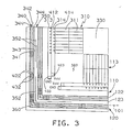
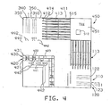
- FIGs. 3-5 show an expanded view of a small portion of chip 100, as indicated by the dotted line 200 in Fig. 2.
- Fig. 3 is primarily drawn at the first of three metal interconnection layers over the cells in rings 113 and 122. For visual reference, however, it also delineates the cell boundaries in the underlying semiconductor layers.
- Fig. 4 is drawn to the same scale, and shows the second metal layer.
- the first digit of the reference numerals are the same as their Figure numbers.
- ring 113 has four arms 310, each comprising a series of long, thin individual I/O cells 311. These cells are placed in pairs, end to end. Discretionary first-metal wiring within each cell personalizes it to perform a particular function. For clarity, this wiring has been omitted from Fig. 3; see Fig. 6. At the sides of each pair, second-metal power Vdd (positive voltage) straps 411 and ground straps 413 run the length of both cells. Heavy first-metal Vdd bus 314 collects the straps 411 through vias 414; first-metal ground bus 313 collects the straps 413 through vias 412. Vias 412 and 414 extend downward from second metal through a conventional insulating layer (not shown) to first metal.
- Vdd positive voltage
- Inner area 450 of the second metal layer contains a Vdd plane 451 having a large number of vias 512 to C4 contacts above the third-metal layer of Fig. 5. Straps 411 tie plane 451 to ground bus 314 as previously described. Inner area 510 of the third metal layer contains a ground plane 511 having multiple vias 514 for connection upward to additional C4 contacts for ground potential. Vias 515 downward to second metal tie ground plane 511 to ground straps 413. Moats 513 in plane 511 isolate vias 512 from plane 511. These large, centrally located Vdd and ground planes, having multiple off-chip contacts, can distribute relatively large currents directly to the I/O cells, and thence by way of multiple parallel straps to busses feeding the remainder of the chip cells. This power-distribution geometry has low losses, low noise, and yet a low interference with other chip wiring.
- Corner region 320 between the arms 310 of ring 113 are not used in first metal, although they could be filled with more cells or wiring if desired.
- Inner region 330 is not needed for power planes. It can be used for test circuits, voltage converters, or other circuits (not shown). These circuits may or may not be laid out in cellular form, and can connect to I/O contacts by means of additional vias (not shown) through the Vdd and ground planes.
- each ring 122 has four arms 340 of logic cells 341 arranged in pairs. Each cell has discretionary wiring in first metal to personalize its function. For clarity, this intra-cell wiring is not shown in Fig. 3; examples can be found in the cited application Ser. No. 457,324 to J. M. Fitzgerald.
- a Vdd bus 342 runs down the backbone of arms 340, preferably continuous in corner areas 360 to form a complete loop around each ring 122.
- a ground bus 344 runs down each edge 343 of arms 340, adjacent wiring-bay arms 350.
- the chip has a total of four heavy second-metal Vdd power busses 420, such as bus 421 in Fig.
- busses 430 running perpendicular to first-metal logic-ring busses 344, coupling to them by vias 422.
- busses 430 such as bus 431, run alongside busses 420, and couple to wiring-bay ground busses 344 through vias 432.
- Busses 420 connect to Vdd power busses 314 through vias 423 in corner areas 320.
- busses 430 couple to ground power busses 313 through vias 433.
- the connections established by vias 423 and 433 also cause busses 313 and 314 to form a complete loop, for lower losses, lower noise, and better load balancing.
- Each logic cell has an edge 343 facing one arm 350 of a wiring bay 123.
- Signal inputs and outputs pass across the cell edges into the wiring-bay arms by means of short conductors (not shown) in a polysilicon layer below first metal. (Alternatively, first or second metal could connect signal wiring to the cells.)
- First-metal signal conductors 352 couple to these short conductors through vias such as 353.
- the first-metal wiring-bay conductors all run parallel to the bay they occupy -- and thus parallel to the adjacent logic-cell arms, they may bend around corners at the ends of the arms, and thus continue for any length in a ring 123.
- the annular chip configuration avoids the tendency of prior-art columnar chips to have wiring jams in the middle of the wiring bays and underutilization at the ends. Corner areas 360 could be filled in with cells or wiring, although this would probably not be practical.
- Second-metal signal wiring 440 is not constrained to run in discrete wiring bays or areas, since no intra-cell connections are made at this level. For visual reference, however, the locations of arms 340 and 350 are partially indicated by dotted lines in Fig. 4. Individual second-metal conductors 441 run perpendicular to first-metal conductors 352, and connect to them through vias such as 442. And, since conductors 352 bend at corners 360, conductors 441 can also change direction there, as at 443. It is also possible to connect second-level metal directly to logic-cell I/Os at edges 343 by vias (not shown). I/O cells 113 are constructed to have signal connections in a wiring bay 350 just outside Vdd bus 314. These connections are wired in the same manner as the external connections of logic cells 341.
- Conductors 521 in third-metal signal wiring 520 then, run above and parallel to cell arms 340 and wiring bays 350, portions of which are shown in dotted lines for visual reference.
- Signal wiring 520 is confined to outer area 120, that is, outside boundary line 102.
- restrictions on the direction and placement of conductors 521 is for the conven-ience of having orderly wiring rules, since no cell wiring extends to this level.
- Conductors 521 may bend around corner areas, as at 522, in the same way as first-level wiring 350. They connect to second-level wiring 440 through vias such as 523.
- Central area 110 is actually defined by the extent of signal-pad wiring 530, as indicated by the dashed line 101 in Fig. 5.
- Individual conductors 531 connect to an intra-cell I/O bus in second metal by vias 532, as will be shown in Fig. 6.
- the other ends of these conductors form pads 533 for solder-ball contacts 112, Fig. 1.
- Wiring 530 is not constrained to a single direction. This is one of the advantages of having a third metal layer in the invention. And, by confining the wiring between I/O cells in area 110 and logic cells in area 120 to second-metal wiring 440, the pad wiring 530 can be laid out independently of the inter-area wiring requirements. That is, wiring 530 can be laid out almost as though it were on a separate chip.
- central area 110 overhangs logic-cell and wiring-bay arms 340 and 350 to some extent.
- third-metal signal wiring is preferably prohibited, although it could be merely limited some what. Since fewer logic cells occupy the inner rings 122, fewer signal connections are required there in any event. In most chips, the area required for pads and pad wiring exceeds the area of the I/O cells, so the ability of the present configuration to overhang the logic cells is a significant advantage.
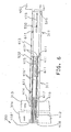
- FIG. 6 details a pair of I/O cells 311 at the second-metal level.
- first-metal power busses 313 and 314 are shown in dotted lines, as are the outlines of the individual cells below first metal.
- Vdd power strap 411 runs from Vdd plane 451 to via 414, which leads to Vdd bus 314.
- Each cell 311 derives its Vdd voltage from this strap at points defined by the particular cell personality, such as at vias 611 descending to first metal or to polysilicon.
- ground strap 413 runs from via 515 to ground plane 511, Fig.5, to via 412, leading down to ground bus 313.
- Personality-dependent vias such as 612 couple growing potential to the individual cells 311.
- the FETs of cells 311 lie below first metal, and all intra-cell wiring (not shown) is at or below first metal in the cell areas.
- Inputs and outputs to the pad wiring 530 are made at any position along the length of I/O rails 613, by vias 532 as described previously. These rails couple to the cell circuitry by personality-dependent vias such as 614 to first metal or polysilicon. Signal inputs and outputs to logic cells 341 are made by leads 614 in second metal. These leads extend from the cell edges at 615, where they connect to intra-cell circuits. They end at locations 616 at the edge of the innermost wiring bay 350.
Landscapes
- Design And Manufacture Of Integrated Circuits (AREA)
- Internal Circuitry In Semiconductor Integrated Circuit Devices (AREA)
- Semiconductor Integrated Circuits (AREA)
Applications Claiming Priority (2)
| Application Number | Priority Date | Filing Date | Title |
|---|---|---|---|
| US06/789,594 US4731643A (en) | 1985-10-21 | 1985-10-21 | Logic-circuit layout for large-scale integrated circuits |
| US789594 | 1985-10-21 |
Publications (3)
| Publication Number | Publication Date |
|---|---|
| EP0220444A2 true EP0220444A2 (de) | 1987-05-06 |
| EP0220444A3 EP0220444A3 (en) | 1989-07-19 |
| EP0220444B1 EP0220444B1 (de) | 1992-07-08 |
Family
ID=25148105
Family Applications (1)
| Application Number | Title | Priority Date | Filing Date |
|---|---|---|---|
| EP86112435A Expired EP0220444B1 (de) | 1985-10-21 | 1986-09-09 | Anordnung logischer Schaltungen für hochintegrierte Schaltung |
Country Status (5)
| Country | Link |
|---|---|
| US (1) | US4731643A (de) |
| EP (1) | EP0220444B1 (de) |
| JP (1) | JPH0691225B2 (de) |
| CA (1) | CA1243423A (de) |
| DE (1) | DE3685931T2 (de) |
Cited By (3)
| Publication number | Priority date | Publication date | Assignee | Title |
|---|---|---|---|---|
| EP0461313A1 (de) * | 1990-06-12 | 1991-12-18 | Fujitsu Limited | Dynamische Speichereinrichtung mit wahlfreiem Zugriff |
| AU653521B2 (en) * | 1990-04-26 | 1994-10-06 | Beecham Group Plc | Use of 5-HT4 receptor antagonists in the treatment of arrythmias and stroke |
| EP1608009A4 (de) * | 2003-02-19 | 2010-05-19 | Sony Corp | Halbleiterbauelement |
Families Citing this family (18)
| Publication number | Priority date | Publication date | Assignee | Title |
|---|---|---|---|---|
| US4910574A (en) * | 1987-04-30 | 1990-03-20 | Ibm Corporation | Porous circuit macro for semiconductor integrated circuits |
| US5045913A (en) * | 1990-01-29 | 1991-09-03 | International Business Machines Corp. | Bit stack compatible input/output circuits |
| US4988636A (en) * | 1990-01-29 | 1991-01-29 | International Business Machines Corporation | Method of making bit stack compatible input/output circuits |
| US5526279A (en) * | 1994-09-22 | 1996-06-11 | International Business Machines Corporation | Nested overlap removal for physical design data using frames |
| US5631842A (en) * | 1995-03-07 | 1997-05-20 | International Business Machines Corporation | Parallel approach to chip wiring |
| JP3432963B2 (ja) * | 1995-06-15 | 2003-08-04 | 沖電気工業株式会社 | 半導体集積回路 |
| US6344667B1 (en) * | 1998-03-02 | 2002-02-05 | Kabushiki Kaisha Toshiba | Wiring board with reduced radiation of undesired electromagnetic waves |
| US6083271A (en) * | 1998-05-05 | 2000-07-04 | Lsi Logic Corporation | Method and apparatus for specifying multiple power domains in electronic circuit designs |
| JP3380465B2 (ja) | 1998-06-29 | 2003-02-24 | 松下電器産業株式会社 | 半導体装置 |
| US6310398B1 (en) | 1998-12-03 | 2001-10-30 | Walter M. Katz | Routable high-density interfaces for integrated circuit devices |
| JP2001217380A (ja) * | 2000-02-04 | 2001-08-10 | Hitachi Ltd | 半導体装置およびその製造方法 |
| WO2003094203A2 (en) * | 2002-04-29 | 2003-11-13 | Silicon Pipe, Inc. | Direct-connect signaling system |
| US7750446B2 (en) | 2002-04-29 | 2010-07-06 | Interconnect Portfolio Llc | IC package structures having separate circuit interconnection structures and assemblies constructed thereof |
| US6891272B1 (en) | 2002-07-31 | 2005-05-10 | Silicon Pipe, Inc. | Multi-path via interconnection structures and methods for manufacturing the same |
| DE10252058A1 (de) * | 2002-11-08 | 2004-05-27 | Infineon Technologies Ag | Halbleiteranordnung |
| US7014472B2 (en) * | 2003-01-13 | 2006-03-21 | Siliconpipe, Inc. | System for making high-speed connections to board-mounted modules |
| US7075179B1 (en) * | 2004-12-17 | 2006-07-11 | Lsi Logic Corporation | System for implementing a configurable integrated circuit |
| US8813016B1 (en) * | 2013-01-28 | 2014-08-19 | Taiwan Semiconductor Manufacturing Company Limited | Multiple via connections using connectivity rings |
Family Cites Families (8)
| Publication number | Priority date | Publication date | Assignee | Title |
|---|---|---|---|---|
| DE2037636A1 (de) * | 1970-07-29 | 1972-02-10 | Philips Patentverwaltung | Integrierte monolithische Halbleiter schaltung mit geregelter Kristalltemperatur |
| US3751720A (en) * | 1971-12-20 | 1973-08-07 | Ibm | Radially oriented monolithic circuit masterslice |
| US3795845A (en) * | 1972-12-26 | 1974-03-05 | Ibm | Semiconductor chip having connecting pads arranged in a non-orthogonal array |
| DE2407696C3 (de) * | 1974-02-18 | 1979-02-01 | Siemens Ag, 1000 Berlin Und 8000 Muenchen | Thyristor |
| JPS5378185A (en) * | 1976-12-22 | 1978-07-11 | Fujitsu Ltd | Integrated circuit logical element |
| JPS593950A (ja) * | 1982-06-30 | 1984-01-10 | Fujitsu Ltd | ゲ−トアレイチツプ |
| US4575744A (en) * | 1983-09-16 | 1986-03-11 | International Business Machines Corporation | Interconnection of elements on integrated circuit substrate |
| JPS60121756A (ja) * | 1983-12-06 | 1985-06-29 | Toshiba Corp | 半導体集積回路装置 |
-
1985
- 1985-10-21 US US06/789,594 patent/US4731643A/en not_active Expired - Fee Related
-
1986
- 1986-05-05 CA CA000508411A patent/CA1243423A/en not_active Expired
- 1986-09-09 EP EP86112435A patent/EP0220444B1/de not_active Expired
- 1986-09-09 DE DE8686112435T patent/DE3685931T2/de not_active Expired - Fee Related
- 1986-09-12 JP JP61214234A patent/JPH0691225B2/ja not_active Expired - Lifetime
Cited By (3)
| Publication number | Priority date | Publication date | Assignee | Title |
|---|---|---|---|---|
| AU653521B2 (en) * | 1990-04-26 | 1994-10-06 | Beecham Group Plc | Use of 5-HT4 receptor antagonists in the treatment of arrythmias and stroke |
| EP0461313A1 (de) * | 1990-06-12 | 1991-12-18 | Fujitsu Limited | Dynamische Speichereinrichtung mit wahlfreiem Zugriff |
| EP1608009A4 (de) * | 2003-02-19 | 2010-05-19 | Sony Corp | Halbleiterbauelement |
Also Published As
| Publication number | Publication date |
|---|---|
| JPS6298745A (ja) | 1987-05-08 |
| JPH0691225B2 (ja) | 1994-11-14 |
| US4731643A (en) | 1988-03-15 |
| DE3685931D1 (de) | 1992-08-13 |
| DE3685931T2 (de) | 1993-02-25 |
| CA1243423A (en) | 1988-10-18 |
| EP0220444A3 (en) | 1989-07-19 |
| EP0220444B1 (de) | 1992-07-08 |
Similar Documents
| Publication | Publication Date | Title |
|---|---|---|
| US4731643A (en) | Logic-circuit layout for large-scale integrated circuits | |
| EP0219668B1 (de) | Logischer Schaltungsentwurf für hochintegrierte Schaltkreise | |
| JP4562908B2 (ja) | Asic配線アーキテクチャ | |
| US6613611B1 (en) | ASIC routing architecture with variable number of custom masks | |
| US4568961A (en) | Variable geometry automated universal array | |
| JP4088587B2 (ja) | 集積回路 | |
| US4499484A (en) | Integrated circuit manufactured by master slice method | |
| US5892276A (en) | Semiconductor integrated circuit | |
| US6306744B1 (en) | Filter capacitor construction | |
| US6114903A (en) | Layout architecture for core I/O buffer | |
| US7146596B2 (en) | Integrated circuit chip having a ringed wiring layer interposed between a contact layer and a wiring grid | |
| US6671865B1 (en) | High density input output | |
| US6897555B1 (en) | Integrated circuit package and method for a PBGA package having a multiplicity of staggered power ring segments for power connection to integrated circuit die | |
| US6744081B2 (en) | Interleaved termination ring | |
| EP0021661A1 (de) | Masterslice-Halbleitervorrichtung | |
| US4575745A (en) | Tailorable standard cells and method for tailoring the performance of IC designs | |
| US6747349B1 (en) | Termination ring for integrated circuit | |
| EP0135019B1 (de) | Verbindung von Elementen auf ein Substrat mit integrierter Schaltung | |
| US5945696A (en) | Silicon chip having mixed input/output slot structure | |
| US5206529A (en) | Semiconductor integrated circuit device | |
| US6828682B1 (en) | Substrate voltage connection | |
| JPS59132144A (ja) | 半導体集積回路装置の製造方法 | |
| JPH01152642A (ja) | 半導体集積回路 | |
| JPS6248042A (ja) | マスタ−スライス方式半導体集積回路 | |
| JPH0480534B2 (de) |
Legal Events
| Date | Code | Title | Description |
|---|---|---|---|
| PUAI | Public reference made under article 153(3) epc to a published international application that has entered the european phase |
Free format text: ORIGINAL CODE: 0009012 |
|
| AK | Designated contracting states |
Kind code of ref document: A2 Designated state(s): DE FR GB IT |
|
| 17P | Request for examination filed |
Effective date: 19870821 |
|
| PUAL | Search report despatched |
Free format text: ORIGINAL CODE: 0009013 |
|
| AK | Designated contracting states |
Kind code of ref document: A3 Designated state(s): DE FR GB IT |
|
| RHK1 | Main classification (correction) |
Ipc: H01L 23/52 |
|
| 17Q | First examination report despatched |
Effective date: 19910403 |
|
| GRAA | (expected) grant |
Free format text: ORIGINAL CODE: 0009210 |
|
| AK | Designated contracting states |
Kind code of ref document: B1 Designated state(s): DE FR GB IT |
|
| PG25 | Lapsed in a contracting state [announced via postgrant information from national office to epo] |
Ref country code: IT Free format text: LAPSE BECAUSE OF FAILURE TO SUBMIT A TRANSLATION OF THE DESCRIPTION OR TO PAY THE FEE WITHIN THE PRESCRIBED TIME-LIMIT;WARNING: LAPSES OF ITALIAN PATENTS WITH EFFECTIVE DATE BEFORE 2007 MAY HAVE OCCURRED AT ANY TIME BEFORE 2007. THE CORRECT EFFECTIVE DATE MAY BE DIFFERENT FROM THE ONE RECORDED. Effective date: 19920708 |
|
| REF | Corresponds to: |
Ref document number: 3685931 Country of ref document: DE Date of ref document: 19920813 |
|
| ET | Fr: translation filed | ||
| PLBE | No opposition filed within time limit |
Free format text: ORIGINAL CODE: 0009261 |
|
| STAA | Information on the status of an ep patent application or granted ep patent |
Free format text: STATUS: NO OPPOSITION FILED WITHIN TIME LIMIT |
|
| 26N | No opposition filed | ||
| PGFP | Annual fee paid to national office [announced via postgrant information from national office to epo] |
Ref country code: DE Payment date: 19950921 Year of fee payment: 10 |
|
| PGFP | Annual fee paid to national office [announced via postgrant information from national office to epo] |
Ref country code: FR Payment date: 19960909 Year of fee payment: 11 |
|
| PG25 | Lapsed in a contracting state [announced via postgrant information from national office to epo] |
Ref country code: DE Effective date: 19970603 |
|
| PGFP | Annual fee paid to national office [announced via postgrant information from national office to epo] |
Ref country code: GB Payment date: 19970812 Year of fee payment: 12 |
|
| PG25 | Lapsed in a contracting state [announced via postgrant information from national office to epo] |
Ref country code: FR Free format text: THE PATENT HAS BEEN ANNULLED BY A DECISION OF A NATIONAL AUTHORITY Effective date: 19970930 |
|
| REG | Reference to a national code |
Ref country code: FR Ref legal event code: ST |
|
| PG25 | Lapsed in a contracting state [announced via postgrant information from national office to epo] |
Ref country code: GB Free format text: LAPSE BECAUSE OF NON-PAYMENT OF DUE FEES Effective date: 19980909 |
|
| GBPC | Gb: european patent ceased through non-payment of renewal fee |
Effective date: 19980909 |