EP0221104B1 - Spannungsmultipliziererschaltung - Google Patents
Spannungsmultipliziererschaltung Download PDFInfo
- Publication number
- EP0221104B1 EP0221104B1 EP86902626A EP86902626A EP0221104B1 EP 0221104 B1 EP0221104 B1 EP 0221104B1 EP 86902626 A EP86902626 A EP 86902626A EP 86902626 A EP86902626 A EP 86902626A EP 0221104 B1 EP0221104 B1 EP 0221104B1
- Authority
- EP
- European Patent Office
- Prior art keywords
- node
- clock signal
- output
- stage
- circuit
- Prior art date
- Legal status (The legal status is an assumption and is not a legal conclusion. Google has not performed a legal analysis and makes no representation as to the accuracy of the status listed.)
- Expired - Lifetime
Links
Images




Classifications
-
- G—PHYSICS
- G11—INFORMATION STORAGE
- G11C—STATIC STORES
- G11C17/00—Read-only memories programmable only once; Semi-permanent stores, e.g. manually-replaceable information cards
-
- H—ELECTRICITY
- H02—GENERATION; CONVERSION OR DISTRIBUTION OF ELECTRIC POWER
- H02M—APPARATUS FOR CONVERSION BETWEEN AC AND AC, BETWEEN AC AND DC, OR BETWEEN DC AND DC, AND FOR USE WITH MAINS OR SIMILAR POWER SUPPLY SYSTEMS; CONVERSION OF DC OR AC INPUT POWER INTO SURGE OUTPUT POWER; CONTROL OR REGULATION THEREOF
- H02M3/00—Conversion of DC power input into DC power output
- H02M3/02—Conversion of DC power input into DC power output without intermediate conversion into AC
- H02M3/04—Conversion of DC power input into DC power output without intermediate conversion into AC by static converters
- H02M3/06—Conversion of DC power input into DC power output without intermediate conversion into AC by static converters using resistors or capacitors, e.g. potential divider
- H02M3/07—Conversion of DC power input into DC power output without intermediate conversion into AC by static converters using resistors or capacitors, e.g. potential divider using capacitors charged and discharged alternately by semiconductor devices with control electrode, e.g. charge pumps
- H02M3/073—Charge pumps of the Schenkel-type
-
- G—PHYSICS
- G11—INFORMATION STORAGE
- G11C—STATIC STORES
- G11C5/00—Details of stores covered by group G11C11/00
- G11C5/14—Power supply arrangements, e.g. power down, chip selection or deselection, layout of wirings or power grids, or multiple supply levels
- G11C5/145—Applications of charge pumps; Boosted voltage circuits; Clamp circuits therefor
Definitions
- the present invention relates to voltage multiplier circuits, and more particularly to voltage pump circuits employed in integrated circuits such as electrically erasable programmable read only memories (EEPROMs).
- EEPROMs electrically erasable programmable read only memories
- EEPROM devices typically employ floating gate transistors, programmed either to the depletion or enhancement mode, as the memory elements.
- a high programming voltage typically about 17 volts, is required to induce electron tunneling to or from the floating gate. If the device is to be operated from a +5 volt supply, a circuit is required to generate an additional 12 volts. This supply circuit should also be capable of charging the large memory circuit capacitance in less than the element programming time (typically 1 millisecond).
- CMOS technology it is known in CMOS technology to use inverting circuits comprising N channel transistors and capacitors, wherein the capacitors are charged in parallel and then connected in series to achieve voltage multiplication.
- the N channel transistors require P wells, which leads to several disadvantages, i.e., more chip area for an equivalent stage, less efficiency due to parasitic capacitance and an undesirable parasitic bipolar NPN device.
- the P wells typically require more separation between stages and therefore require a larger chip area to maintain an equivalent output current.
- the P wells introduce a parasitic capacitance which may be charged and discharged each cycle, thereby reducing efficiency.
- the possibility of latch-up is introduced by the addition of a bipolar NPN device. This is a serious disadvantage to newer processes which are more sensitive to latch-up.
- a voltage multiplier circuit having an input node and an output node, comprising transfer clock means for providing a transfer clock signal, pump clock means for providing a pump clock signal having high and low states, pump capacitor means for capacitively coupling said pump clock to said output node, switching means for selectively coupling the output node to the input node in response to said transfer clock signal, and whereby said transfer clock signal and said switching means are cooperatively adapted to couple said input node to said output node during an interval when said pump clock is at said high state so as to equalize the potential between said input and output node, and to isolate said input and output nodes during an interval when said pump clock is at its low state, characterized in that said transfer clock signal is capacitively coupled to said switching means.
- each stage can be cascaded together to generate a large negative voltage from a clock signal of positive polarity, for example, to develop the programming voltage for an integrated circuit such as an EEPROM.
- the transistor elements for the circuit are preferably p-channel enhancement mode devices.
- the input node of the first stage is coupled to ground, and the output node is coupled to the input node of the next stage.
- a rectifying stage is coupled to the output node of the final stage.
- each stage is provided with a means to reset the DC bias on the gate of the transistor to the input node potential.
- First and second non-overlapping pump and transfer clocks 180° out of phase, are provided to drive alternate stages of the cascaded multiplier circuit. This ensures that the switching transistors of adjacent stages are not in the conductive state at the same time.
- the present invention comprises a novel voltage multiplier.
- the following description is presented to enable any person skilled in the art to make and use the invention, and is provided in the context of a particular application and its requirements. Various modifications to the preferred embodiment will be readily apparent to those skilled in the art, and the generic principles defined herein may be applied to other embodiments and applications.
- the circuit comprises a diode rectifier R D coupled cathode to anode between the circuit input node and its output node, and a pump capacitor C D coupling the output node to a pump clock signal.
- the input voltage V in to the circuit is applied at the input node, and the circuit output voltage V out is taken at its output node.
- the pump clock is a square wave signal having a low state (0 volts) and a high state (+V DD volts).
- V out is initially 0 volts.
- the pump clock signal pulses high to V DD .
- the voltage V out is capacitively coupled to +V DD , but decays through the forward biased rectifier diode R D to ground, charging capacitor C D to ⁇ V DD .
- the pump clock signal pulses low, the voltage V out is coupled to -V DD and R D is reverse biased to the non-conductive state, preventing C D from discharging.
- V out is now about equal to V in -V DD .
- each stage has a charge pumping capacitor C D which couples the pump clock signal to the output node.
- C D When a positive voltage with respect to V in occurs at V out , C D is charged through the rectifier R o to V IN ⁇ V DD .
- V out When the pump clock signal transitions to its low level, V out is coupled to V IN -V DD .
- the available diodes either have one terminal tied to a supply voltage or contain a parasitic bipolar NPN transistor that conducts large currents when the diode is forward biased. For these reasons, the available diodes may not be used as the rectifier element for the voltage multiplier circuit.
- the rectifier is replaced by a circuit employing a clocked transistor, to perform a function analogous to that performed by the rectifier.
- the transfer clock is capacitively coupled to the gate of the rectifying transistor, and the D.C. voltage applied to the gate is reset between each cycle.
- the rectifying transistor is clocked by a transfer clock with high and low levels adapted to turn the transistor on or off, irrespective of the degree of negative potential at node V in .
- the transfer clock signal states are preferably at ground and the positive supply level (V DD ).
- a novel aspect of the invention is that the rectifying transistor is gated to the conductive and nonconductive states by a transfer clock signal with states at ground and the supply potential, even though the output node may be substantially more negative than the supply potential.
- the transistors T1, T2, and T3 are p-channel enhancement mode devices. In order for these devices to be in the conductive state, the gate potential must be lower than either the drain or source potential by at least a threshold voltage, on the order of 1 volt.
- Transistor T1 is coupled between the gate of transistor T2 and node V IN and provides a means for selectively resetting the voltage at node V A , the gate potential for transistor T1, to V 1N , thus providing a D.C. reference for node V A .
- the pump clock signal ⁇ P pulses high. This voltage change is coupled to node V OUT and to node V B via capacitors C3 and C2, respectively. Since the potential at node V A is less than the potential at node V ouT , the p-channel enhancement transistor T2 turns on and charges capacitor C3 toward -(V DD -V IN ). When V OUT reaches a potential equivalent to a threshold voltage above the potential at node V A , transistor T2 turns off.
- the pump clock signal ⁇ P pulses low, pulling the potential at the nodes V OUT and V B to ⁇ (V IN- V DD ),
- capacitor C3 will discharge during the time interval between times t 4 and t 5 .
- Node V B is isolated from the load, and hence its potential stays constant during this time interval.
- the current capacity of the circuit is increased due to the isolation of V B from the load, as will be discussed in more detail below. Since the voltage at V B is less than the voltage at V 1N , T1 is turned on, resetting V A to V IN while the pump clock signal ⁇ P is low. This in turn maintains transistors T2 and T3 in the nonconductive state.
- the next cycle starts at time t s when the pump clock signal ⁇ P pulses high.
- This pulse is coupled to node V B through the capacitor C2, raising the voltage at node V B from ⁇ (VDD ⁇ V IN ) to V IN volts.
- This turns transistor T1 off, isolating node V A from node V IN so that the potential at node V A can be pulsed low by the transfer clock signal ⁇ t at time t 6 .
- the node V OUT With the pump clock signal ⁇ P at +V DD , the node V OUT will be coupled at a positive voltage with respect to the potential at node V IN .
- the potential difference between the two nodes is determined by the amount that capacitor C3 discharged in the time interval between t 4 and t s . If the amount of discharge between cycles is small, the potential at node V OUT will be slightly more positive than the potential at node V IN , and transistor T2 will not turn on until time t 6 , when the transfer clock signal ⁇ t pulses low. From this point on, the operation of the circuit repeats.
- the transistor T3 and capacitor C2 may be omitted from the circuit, and the base of transistor T1 coupled directly to the node V OUT as illustrated by the phantom line connection A shown in Figure 1.
- the circuit will perform satisfactorily with these modifications, and in fact the operation is identical when the circuit operation is at steady state with no resistive loading or when operated with a very low rate clock.
- the advantage of employing the more complex circuit of Figure 1, with its isolation of the control node V B from the output node V OUT is that the circuit may be clocked at a faster rate than if the node V B were simply coupled directly to the node V OUT .
- the operation of the transistor T3 and the capacitor C2 in the circuit of Figure 1 mimics that of the transistor T2 and the capacitor C3, except that the capacitor C2 is not coupled to the load at node V OUT , and therefore is not discharged under DC load conditions.
- the capacitor C3 With the capacitor C3 fully charged, the drive on the transistor T1 is maintained, keeping the transistor in the conductive state and allowing the node V A to discharge to the potential at the node V IN much more quickly under loaded conditions than if the gate of transistor T1 were driven by the potential at node V OUT .
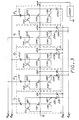
- Each stage of the multiplier circuit comprises six devices, the three capacitors C1N, C2N and C3N, and three p-channel MOS transistors.
- stage 1 through 4 add in series to generate a negative voltage about equal to four times the peak to peak voltage of the clock signals.
- the last stage 5 acts as a rectifier stage, isolating V04 from V05 when V04 is more positive than V05.
- the rectifier stage 5 is identical to stages 1 ⁇ 4, except that the pumping capacitor C3N for the stage is omitted.
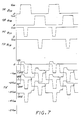
- the four stages are alternately connected to the sources of pump and transfer clock signals ⁇ PA , ⁇ PB , ⁇ TA , ⁇ TB , which are respectively 180° out of phase, as shown in Figures 4A-4D.
- Figure 4E illustrates the steady-state signal waveforms of the output nodes VON at each stage of the cascaded circuit of Figure 3, with no resistive load on the circuit output V05. Since the clock signals are capacitively coupled to the respective stages, the circuit operation is essentially the same as described above with respect to the single stage circuit shown in Figure 1.
- Figures 4A-4D are waveform timing diagrams of the transfer clock signals ⁇ TA and ⁇ TB and the pump clock signals ⁇ PA and ⁇ PB .
- the transfer clock signals ⁇ TA and ⁇ TB are non-overlapping clock signals in that neither clock is high at the same time the other clock signal is high.
- the pump clock signals ⁇ PA and ⁇ PB are non-overlapping signals. Circuits to generate these types of non-overlapping clock signals are known in the art, and for that reason are not described herein.
- the rectifying transistor T2N When the output node VO(N-1) of the previous stage is pulsed high, the rectifying transistor T2N remains turned off because the transistor T1 N holds the gate of the rectifying transistor T2N at the input voltage to the stage at node VO(N-1).
- Figure 5E illustrates the waveforms at the control nodes VAN for the cascaded circuit of Figure 3 under the same conditions as apply to the Figure 4E waveforms, namely steady-state and no resistive load.
- FIGS 6E, 7E and 8E illustrate, respectively, the waveforms at the output nodes VON, the nodes VAN and the nodes VBN for the cascaded circuit of Figure 3, under steady-state, resistive load conditions.
- the output voltage at node V05 generated by the multiplier circuit is dependent on the circuit loading.
- the steady-state voltage at node V05 is very nearly -4V DD , as shown in Figure 4E.
- the output voltage at node V05 is reduced, and its value depends on the loading.
- the input node of the first stage of the embodiment of Figure 3 is connected to ground, this is not a requirement for proper operation of the circuit.
- the first stage input node may be connected, for example, to a negative supply potential and the multiplier circuit will operate to pump down to an output voltage more negative than this supply potential.
- the pump clock signal is not required to have states at 0 volts and the positive supply level.
- the circuit will operate, e.g., with states of -V DD and + VDD .
- the positive state may be at a level below V DD ; however, more stages will be required to reach a desired output potential.
- capacitors C1N have a nominal value of 6 picofarads, capacitors C2N a nominal value of 2 picofarads, and C3N a nominal value of 95 picofarads.
- the value of C1 N is selected to be about ten times the gate capacitance of transistor T2N. The larger the capacitance of C3N, the greater is the current sinking capability of the circuit, but at the expense of chip area.
- the effective impedance of the four-stage multiplier circuit of Figure 3 is proportional to both the pump clock signal frequency and the capacitance C3N. For nominal values of 500 KHz for the clock frequency and 95 picofarads for C3N, the effective impedance is in the range of 100 Kohms.
Landscapes
- Engineering & Computer Science (AREA)
- Power Engineering (AREA)
- Dc-Dc Converters (AREA)
- Read Only Memory (AREA)
Claims (17)
Applications Claiming Priority (2)
| Application Number | Priority Date | Filing Date | Title |
|---|---|---|---|
| US06/728,731 US4734599A (en) | 1985-04-30 | 1985-04-30 | Circuit for multiplying a pump clock voltage |
| US728731 | 1985-04-30 |
Publications (2)
| Publication Number | Publication Date |
|---|---|
| EP0221104A1 EP0221104A1 (de) | 1987-05-13 |
| EP0221104B1 true EP0221104B1 (de) | 1990-07-18 |
Family
ID=24928069
Family Applications (1)
| Application Number | Title | Priority Date | Filing Date |
|---|---|---|---|
| EP86902626A Expired - Lifetime EP0221104B1 (de) | 1985-04-30 | 1986-03-31 | Spannungsmultipliziererschaltung |
Country Status (7)
| Country | Link |
|---|---|
| US (1) | US4734599A (de) |
| EP (1) | EP0221104B1 (de) |
| JP (1) | JPS62502223A (de) |
| KR (1) | KR900008187B1 (de) |
| DE (1) | DE3672748D1 (de) |
| HK (1) | HK93490A (de) |
| WO (1) | WO1986006539A2 (de) |
Families Citing this family (22)
| Publication number | Priority date | Publication date | Assignee | Title |
|---|---|---|---|---|
| JPS63290159A (ja) * | 1987-05-20 | 1988-11-28 | Matsushita Electric Ind Co Ltd | 昇圧回路 |
| US5014097A (en) * | 1987-12-24 | 1991-05-07 | Waferscale Integration, Inc. | On-chip high voltage generator and regulator in an integrated circuit |
| NL8800408A (nl) * | 1988-02-18 | 1989-09-18 | Philips Nv | Geintegreerde geheugenschakeling met een hoogspanningsschakelaar tussen een programmeerspanningsgenerator en een wisbaar programmeerbaar geheugen, hoogspanningsschakelaar geschikt voor toepassing in een dergelijke geheugenschakeling. |
| US4807104A (en) * | 1988-04-15 | 1989-02-21 | Motorola, Inc. | Voltage multiplying and inverting charge pump |
| US4931674A (en) * | 1988-11-16 | 1990-06-05 | United States Of America As Represented By The Secretary Of The Navy | Programmable analog voltage multiplier circuit means |
| DE3931596A1 (de) * | 1989-03-25 | 1990-10-04 | Eurosil Electronic Gmbh | Spannungsvervielfacherschaltung |
| JP2531267B2 (ja) * | 1989-06-20 | 1996-09-04 | 日本電気株式会社 | チャ―ジポンプ |
| US5666080A (en) * | 1993-06-17 | 1997-09-09 | Yozan, Inc. | Computational circuit |
| US5617053A (en) * | 1993-06-17 | 1997-04-01 | Yozan, Inc. | Computational circuit |
| CN1109404C (zh) * | 1993-09-20 | 2003-05-21 | 株式会社鹰山 | 计算电路 |
| US5500612A (en) * | 1994-05-20 | 1996-03-19 | David Sarnoff Research Center, Inc. | Constant impedance sampling switch for an analog to digital converter |
| GB2301720B (en) | 1995-06-01 | 2000-05-24 | Motorola Inc | A MOS switching circuit |
| US5587680A (en) * | 1995-06-30 | 1996-12-24 | Mts Systems Corporation | Pulse generator with charge pump |
| US6118326A (en) * | 1997-11-06 | 2000-09-12 | Analog Devices, Inc. | Two-phase bootstrapped CMOS switch drive technique and circuit |
| US5945872A (en) * | 1997-11-06 | 1999-08-31 | Analog Devices, Inc. | Two-phase boosted CMOS switch drive technique and circuit |
| DE59915144D1 (de) * | 1998-09-10 | 2010-05-12 | Infineon Technologies Ag | Ladungspumpenschaltung |
| JP3554497B2 (ja) * | 1998-12-08 | 2004-08-18 | シャープ株式会社 | チャージポンプ回路 |
| DE19926700A1 (de) * | 1998-12-21 | 2000-07-06 | Siemens Ag | Vorrichtung zur Spannungsvervielfachung mit hohem Wirkungsgrad und ihre Verwendung |
| EP1124314B1 (de) * | 2000-02-09 | 2009-01-07 | EM Microelectronic-Marin SA | Ladungspumpenvorrichtung |
| US6492861B2 (en) | 2000-02-09 | 2002-12-10 | Em Microelectronic-Marin Sa | Electronic charge pump device |
| KR100720246B1 (ko) * | 2005-11-17 | 2007-05-22 | 주식회사 하이닉스반도체 | 전파 전압 채배기 및 다단 전파 전압 채배기 |
| WO2009043044A1 (en) * | 2007-09-28 | 2009-04-02 | Maxim Integrated Products, Inc. | A sampling device and circuit having a single voltage supply |
Family Cites Families (5)
| Publication number | Priority date | Publication date | Assignee | Title |
|---|---|---|---|---|
| US3975671A (en) * | 1975-02-24 | 1976-08-17 | Intel Corporation | Capacitive voltage converter employing CMOS switches |
| IT1073440B (it) * | 1975-09-22 | 1985-04-17 | Seiko Instr & Electronics | Circuito elevatore di tensione realizzato in mos-fet |
| JPS5693422A (en) * | 1979-12-05 | 1981-07-29 | Fujitsu Ltd | Level-up circuit |
| JPS56129570A (en) * | 1980-03-14 | 1981-10-09 | Mitsubishi Electric Corp | Booster circuit |
| US4485433A (en) * | 1982-12-22 | 1984-11-27 | Ncr Corporation | Integrated circuit dual polarity high voltage multiplier for extended operating temperature range |
-
1985
- 1985-04-30 US US06/728,731 patent/US4734599A/en not_active Expired - Lifetime
-
1986
- 1986-03-31 KR KR1019860700937A patent/KR900008187B1/ko not_active Expired
- 1986-03-31 JP JP61502087A patent/JPS62502223A/ja active Pending
- 1986-03-31 EP EP86902626A patent/EP0221104B1/de not_active Expired - Lifetime
- 1986-03-31 DE DE8686902626T patent/DE3672748D1/de not_active Expired - Fee Related
- 1986-03-31 WO PCT/US1986/000646 patent/WO1986006539A2/en not_active Ceased
-
1990
- 1990-11-08 HK HK934/90A patent/HK93490A/en not_active IP Right Cessation
Also Published As
| Publication number | Publication date |
|---|---|
| JPS62502223A (ja) | 1987-08-27 |
| DE3672748D1 (de) | 1990-08-23 |
| KR880700432A (ko) | 1988-03-15 |
| KR900008187B1 (ko) | 1990-11-05 |
| US4734599A (en) | 1988-03-29 |
| EP0221104A1 (de) | 1987-05-13 |
| WO1986006539A2 (en) | 1986-11-06 |
| WO1986006539A3 (en) | 1986-12-18 |
| HK93490A (en) | 1990-11-16 |
Similar Documents
| Publication | Publication Date | Title |
|---|---|---|
| US4734599A (en) | Circuit for multiplying a pump clock voltage | |
| EP1237266B1 (de) | Halbleiterspannungserhöhungsschaltung | |
| US4321661A (en) | Apparatus for charging a capacitor | |
| JP2703706B2 (ja) | 電荷ポンプ回路 | |
| US20020122324A1 (en) | High voltage generating charge pump circuit | |
| US4839787A (en) | Integrated high voltage generating system | |
| US5059815A (en) | High voltage charge pumps with series capacitors | |
| KR101039236B1 (ko) | 면적 효율성을 고려한 충전 펌프 및 전압 생성 방법 | |
| JP2528196B2 (ja) | 電圧逓倍回路 | |
| JP3183672B2 (ja) | チャージポンプ装置 | |
| JP3323936B2 (ja) | 上昇率を制御するチャージ・ポンプ | |
| EP0404124B1 (de) | Eine Erhöhungsschaltung enthaltende Ladungspumpe, welche mit zwei Taktimpulssequenzen arbeitet | |
| US6184594B1 (en) | Multi-stage charge pump having high-voltage pump control feedback and method of operating same | |
| US5943271A (en) | Semiconductor integrated circuit device | |
| US6191963B1 (en) | Charge pump with no diode drop at output stage | |
| EP0865149B1 (de) | Starkstrom-CMOS-Ladungspumpe, insbesondere für Flash-EEPROM-Speicher | |
| US4275437A (en) | Semiconductor circuit for voltage conversion | |
| JPS6144414B2 (de) | ||
| EP0836129A1 (de) | Spannungsvervielfacher | |
| JP2000324805A (ja) | チャージポンプ回路 | |
| JPH0430207B2 (de) | ||
| US7148739B2 (en) | Charge pump element with body effect cancellation for early charge pump stages | |
| JP2001245468A (ja) | 昇圧回路 | |
| EP0851562B1 (de) | Hochspannungsladungspumpe,insbesondere für Flash-EEPROM-Speicher | |
| EP0376627A2 (de) | Integrierte Hochspannung erzeugende Einrichtung |
Legal Events
| Date | Code | Title | Description |
|---|---|---|---|
| PUAI | Public reference made under article 153(3) epc to a published international application that has entered the european phase |
Free format text: ORIGINAL CODE: 0009012 |
|
| 17P | Request for examination filed |
Effective date: 19861120 |
|
| AK | Designated contracting states |
Kind code of ref document: A1 Designated state(s): CH DE FR GB IT LI NL |
|
| 17Q | First examination report despatched |
Effective date: 19890207 |
|
| GRAA | (expected) grant |
Free format text: ORIGINAL CODE: 0009210 |
|
| AK | Designated contracting states |
Kind code of ref document: B1 Designated state(s): CH DE FR GB IT LI NL |
|
| REF | Corresponds to: |
Ref document number: 3672748 Country of ref document: DE Date of ref document: 19900823 |
|
| ET | Fr: translation filed | ||
| ITF | It: translation for a ep patent filed | ||
| PLBE | No opposition filed within time limit |
Free format text: ORIGINAL CODE: 0009261 |
|
| STAA | Information on the status of an ep patent application or granted ep patent |
Free format text: STATUS: NO OPPOSITION FILED WITHIN TIME LIMIT |
|
| 26N | No opposition filed | ||
| ITTA | It: last paid annual fee | ||
| PGFP | Annual fee paid to national office [announced via postgrant information from national office to epo] |
Ref country code: FR Payment date: 19990208 Year of fee payment: 14 |
|
| PGFP | Annual fee paid to national office [announced via postgrant information from national office to epo] |
Ref country code: GB Payment date: 19990216 Year of fee payment: 14 |
|
| PGFP | Annual fee paid to national office [announced via postgrant information from national office to epo] |
Ref country code: NL Payment date: 19990224 Year of fee payment: 14 Ref country code: CH Payment date: 19990224 Year of fee payment: 14 |
|
| PGFP | Annual fee paid to national office [announced via postgrant information from national office to epo] |
Ref country code: DE Payment date: 19990226 Year of fee payment: 14 |
|
| REG | Reference to a national code |
Ref country code: GB Ref legal event code: 732E |
|
| PG25 | Lapsed in a contracting state [announced via postgrant information from national office to epo] |
Ref country code: LI Free format text: LAPSE BECAUSE OF NON-PAYMENT OF DUE FEES Effective date: 20000331 Ref country code: GB Free format text: LAPSE BECAUSE OF NON-PAYMENT OF DUE FEES Effective date: 20000331 Ref country code: CH Free format text: LAPSE BECAUSE OF NON-PAYMENT OF DUE FEES Effective date: 20000331 |
|
| PG25 | Lapsed in a contracting state [announced via postgrant information from national office to epo] |
Ref country code: NL Free format text: LAPSE BECAUSE OF NON-PAYMENT OF DUE FEES Effective date: 20001001 |
|
| REG | Reference to a national code |
Ref country code: CH Ref legal event code: PL |
|
| GBPC | Gb: european patent ceased through non-payment of renewal fee |
Effective date: 20000331 |
|
| PG25 | Lapsed in a contracting state [announced via postgrant information from national office to epo] |
Ref country code: FR Free format text: LAPSE BECAUSE OF NON-PAYMENT OF DUE FEES Effective date: 20001130 |
|
| NLV4 | Nl: lapsed or anulled due to non-payment of the annual fee |
Effective date: 20001001 |
|
| REG | Reference to a national code |
Ref country code: FR Ref legal event code: ST |
|
| PG25 | Lapsed in a contracting state [announced via postgrant information from national office to epo] |
Ref country code: DE Free format text: LAPSE BECAUSE OF NON-PAYMENT OF DUE FEES Effective date: 20010103 |
|
| PG25 | Lapsed in a contracting state [announced via postgrant information from national office to epo] |
Ref country code: IT Free format text: LAPSE BECAUSE OF NON-PAYMENT OF DUE FEES;WARNING: LAPSES OF ITALIAN PATENTS WITH EFFECTIVE DATE BEFORE 2007 MAY HAVE OCCURRED AT ANY TIME BEFORE 2007. THE CORRECT EFFECTIVE DATE MAY BE DIFFERENT FROM THE ONE RECORDED. Effective date: 20050331 |