EP0221394A2 - Verfahren zur Herstellung einer integrierten Schaltung - Google Patents
Verfahren zur Herstellung einer integrierten Schaltung Download PDFInfo
- Publication number
- EP0221394A2 EP0221394A2 EP86114064A EP86114064A EP0221394A2 EP 0221394 A2 EP0221394 A2 EP 0221394A2 EP 86114064 A EP86114064 A EP 86114064A EP 86114064 A EP86114064 A EP 86114064A EP 0221394 A2 EP0221394 A2 EP 0221394A2
- Authority
- EP
- European Patent Office
- Prior art keywords
- trenches
- silicon
- substrate
- trench
- layer
- Prior art date
- Legal status (The legal status is an assumption and is not a legal conclusion. Google has not performed a legal analysis and makes no representation as to the accuracy of the status listed.)
- Granted
Links
Images


Classifications
-
- H—ELECTRICITY
- H10—SEMICONDUCTOR DEVICES; ELECTRIC SOLID-STATE DEVICES NOT OTHERWISE PROVIDED FOR
- H10P—GENERIC PROCESSES OR APPARATUS FOR THE MANUFACTURE OR TREATMENT OF DEVICES COVERED BY CLASS H10
- H10P32/00—Diffusion of dopants within, into or out of wafers, substrates or parts of devices
- H10P32/10—Diffusion of dopants within, into or out of semiconductor bodies or layers
- H10P32/14—Diffusion of dopants within, into or out of semiconductor bodies or layers within a single semiconductor body or layer in a solid phase; between different semiconductor bodies or layers, both in a solid phase
- H10P32/1408—Diffusion of dopants within, into or out of semiconductor bodies or layers within a single semiconductor body or layer in a solid phase; between different semiconductor bodies or layers, both in a solid phase from or through or into an external applied layer, e.g. photoresist or nitride layers
- H10P32/141—Diffusion of dopants within, into or out of semiconductor bodies or layers within a single semiconductor body or layer in a solid phase; between different semiconductor bodies or layers, both in a solid phase from or through or into an external applied layer, e.g. photoresist or nitride layers the applied layer comprising oxides only
-
- H—ELECTRICITY
- H10—SEMICONDUCTOR DEVICES; ELECTRIC SOLID-STATE DEVICES NOT OTHERWISE PROVIDED FOR
- H10P—GENERIC PROCESSES OR APPARATUS FOR THE MANUFACTURE OR TREATMENT OF DEVICES COVERED BY CLASS H10
- H10P32/00—Diffusion of dopants within, into or out of wafers, substrates or parts of devices
- H10P32/10—Diffusion of dopants within, into or out of semiconductor bodies or layers
- H10P32/17—Diffusion of dopants within, into or out of semiconductor bodies or layers characterised by the semiconductor material
- H10P32/171—Diffusion of dopants within, into or out of semiconductor bodies or layers characterised by the semiconductor material being group IV material
-
- H—ELECTRICITY
- H10—SEMICONDUCTOR DEVICES; ELECTRIC SOLID-STATE DEVICES NOT OTHERWISE PROVIDED FOR
- H10W—GENERIC PACKAGES, INTERCONNECTIONS, CONNECTORS OR OTHER CONSTRUCTIONAL DETAILS OF DEVICES COVERED BY CLASS H10
- H10W10/00—Isolation regions in semiconductor bodies between components of integrated devices
- H10W10/01—Manufacture or treatment
- H10W10/041—Manufacture or treatment of isolation regions comprising polycrystalline semiconductor materials
-
- H—ELECTRICITY
- H10—SEMICONDUCTOR DEVICES; ELECTRIC SOLID-STATE DEVICES NOT OTHERWISE PROVIDED FOR
- H10W—GENERIC PACKAGES, INTERCONNECTIONS, CONNECTORS OR OTHER CONSTRUCTIONAL DETAILS OF DEVICES COVERED BY CLASS H10
- H10W10/00—Isolation regions in semiconductor bodies between components of integrated devices
- H10W10/40—Isolation regions comprising polycrystalline semiconductor materials
-
- H—ELECTRICITY
- H10—SEMICONDUCTOR DEVICES; ELECTRIC SOLID-STATE DEVICES NOT OTHERWISE PROVIDED FOR
- H10W—GENERIC PACKAGES, INTERCONNECTIONS, CONNECTORS OR OTHER CONSTRUCTIONAL DETAILS OF DEVICES COVERED BY CLASS H10
- H10W20/00—Interconnections in chips, wafers or substrates
- H10W20/01—Manufacture or treatment
- H10W20/021—Manufacture or treatment of interconnections within wafers or substrates
Definitions
- This invention relates to the fabrication of semiconductor integrated circuits.
- this invention is directed to a method of simultaneously forming electrically isolated areas and conductive contact areas in semiconductor material.
- undoped polysilicon trench isolation also does not require the step of passivation layer removal at the trench bottom. Consequently, the trench sidewall is not exposed to etching operations such as reactive ion etching (RIE) and, therefore, does not need additional protective layers such as Si3N4 which also cause additional problems in terms of forming dislocations near trenches in subsequent heat processing steps.
- RIE reactive ion etching
- this invention defines a process which employs undoped polysilicon trench isolation and doped epitaxially grown silicon simultaneously for purposes of substrate contact.
- a borosilicate glass lining is formed on the sidewalls of the trenches in the non-device areas and epitaxially grown silicon is then grown in the trenches.
- Subsequent heating causes the doping of the epitaxially grown silicon with the boron dopant of the borosilicate glass.
- the fill temperature may also provide for dopant movement.
- an undoped epitaxial fill is provided followed by doping of a polysilicon fill material and subsequent planarization by known techniques in chemical/mechanical polishing.
- the initial epitaxial fill may be used for substrate contact while the subsequent polysilicon (undoped) is used to provide device isolation.
- a monocrystalline semiconductor substrate having a pattern of substantially vertical wall trenches extending from a major surface of the substrate into the substrate material.
- An insulator layer is formed on the walls of the trenches.
- a boron ion implantation is then performed to establish the channel stop layer at the bottom of the trench.
- a borosilicate glass layer is then formed on the walls of the isolation layer.
- a portion of the insulator layer is removed together with a portion of the borosilicate glass layer from the bottom by etching techniques.
- One technique is anisotropic etching.
- borosilicate glass layer is removed from all portions of the trenches except where electrical contact is desired.
- the trenches are then filled with silicon to produce a pattern of isolation trenches with undoped silicon in the trenches except where the borosilicate layer is present such that the silicon is doped to provide an electrical contact to the substrate.
- a monocrystalline semiconductor substrate having a pattern of substantially vertical wall trenches extending from a major surface of the substrate and into the substrate structure.
- the substrate and the trenches are lined with SiO2 and boron ions are implanted into the trench bottoms for the formation of a p-doped channel stop.
- the oxide is removed at the bottom of the trenches in those locations where silicon substrate contacts are to be formed.
- the photoresist fills and remains in the trench, thereby protecting the SiO2 lining at the bottom of that trench from the RIE etching.
- epitaxial p-doped silicon is then grown in the trenches designated to be substrate contact areas to slightly overfill these trenches.
- An example of epitaxial growth is described in U.S. Patent 4,526,631.
- Undoped polysilicon is then deposited in all trenches and on the substrate surface. This is followed by planarization of both the p-doped selective epitaxial filled silicon substrate contact trench and the undoped polysilicon isolation trench using known chemical/mechanical polishing techniques.
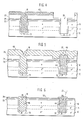
- Figure 1 illustrates an intermediate starting point of this invention wherein the substrate 10 typically comprises a three-tier structure.
- a P-type substrate material 12 has an N+ region 14 which typically serves as a low-resistance contact or collector region beneath an epitaxial layer.
- the third tier is an N-type epitaxial layer formed over the N+ region. This layer serves as the active region for the device. It is in this three-tiered structure that the problem of electrical isolation of portions of those layers occur. This specific problem is solved by this invention.
- thermal SiO2 22 covers the substrate surface in the interior walls of the trenches.
- a layer 24 of Si3N4 is deposited followed by deposition by CVD of a SiO2 layer 26.
- trenches 18 and 20 are opened into the substrate.
- a borosilicate layer is formed as the inside lining of the trench sidewalls.
- This layer 28 is deposited in both trenches 18 and 20.
- the trench bottom 30 is opened, that is, removal of layers 22, 24 and 28 at the bottom of the trench, and a channel stop layer 32 is provided.
- the channel stop may be formed by a variety of known techniques. For example, it may be formed by ion implantation of the bottom surface 30, by lining the inside walls with borosilicate with a subsequent heat treatment for boron out-diffusion or by a combination of the two.
- trench 20 will ultimately become a substrate contact while trench 18 will become the isolation trench. While two trenches are illustrated, it is to be understood that on the substrate 10 an array of such trenches will be present. It is also understood that trench size will vary and may be different between contact and non-contact techniques.
- a preferential etch step is performed to remove the borosilicate trench sidewall everywhere except for the substrate contact areas. As illustrated in Figure 2, the borosilicate 28 remains in the trench 20 while it is removed from the sidewalls of trench 18. This is accomplished by a photoalignment step with a preferential etch to remove the borosilicate trench lining material. Such etch techniques are known in the art.
- trenches 18 and 20 are filled completely with selectively deposited epitaxial silicon (34). This undoped fill material completely fills the trenches 18 and 20.
- the boron, outdiffusing from the previously deposited borosilicate trench lining into the undoped epitaxial silicon in the substrate contact area 32 dopes the epi.
- doping occurs only by outdiffusion of the trench channel stop boron diffusion 32 into the epitaxial silicon near the trench bottom. Consequently, as illustrated in Figure 2, a substrate contact area 36 is created in the trench 20 since the epi is doped.
- the isolation trench 18 the outdiffusion of the channel stop boron is only into the epitaxial silicon near the trench bottom. Such is shown by shallow zone 38 in Figure 2. Consequently, by this technique a series of isolation trenches and a series of substrate contact trenches may be simultaneously formed.
- the structure is completed by SiO2 insulation 19 above trench 18 and metal contact 23 above the contact trench 20.
- thermal SiO2/Si3N4/CVD borosilicate is used as a trench sidewall for doping an undoped epitaxial fill.
- These materials form a permanent sidewall structure that reduces the probability of dislocations which are caused by subsequent heat treatment of a conventional sidewall structure.
- this structure can be: thermal SiO2 approximately 50 nm, Si3N4approximately 50 nm and CVD borosilicate approximately 400 nm in thickness. Other relative thicknesses are within the scope of this invention. Also, other insulation layers may be used in place of this structure.
- FIG. 4 illustrates the structure after an RIE step has opened the trench bottom and removed some of the top oxide layer.
- RIE in a timed etch step to remove oxide from the trench 20 to form the "future" silicon substrate con tact. That is, Figure 4 illustrates a structure having trench 20 with oxide removed such that the trench is opened for contact while trench 18 remains filled with photoresist material. This timed etching also opens the area above trench 20 by selective removal of the CVD oxide 26. The photoresist 40 is then removed.
- a selective epitaxial p-doped silicon zone 44 has been deposited and grown in the substrate contact trench 20.
- This epitaxial silicon refill can be made to slightly overfill trench 20 as illustrated.
- the epitaxial silicon is allowed to grow upward and outward, to completely encapsulate and seal the trench 20.
- Such is illustrated in Figure 5 (structure 46).
- This selective growth occurs only in trenches where a substrate contact opening has been provided at the trench bottom. Application of a blanket growth of undoped polysilicon follows the selective epitaxial refill.
- This layer 48 completely fills the trench 18 and covers the CVD oxide layer 26. It also covers and encapsulates the dome 46 and the epitaxially grown p-doped silicon layer.
- Figure 5 illustrates that when the undoped polysilicon 48 is deposited discontinuities in planarity occur in those areas where trench filling occurs. Ridges are also formed in the vicinity of the cap 46.
- both the p-doped epitaxial dome 46 and the polysilicon undoped material 48 filling the trench 18 are planarized.
- the CVD oxide layer is removed and the domed structure 46 is polished such that planarization of the top surface 50 of the substrate occurs.
- the structure is completed by an SiO2 layer 19 over trench 18 and a metal contact 23 over trench 20.
- an isolation trench 18 is formed filled with undoped polysilicon while, as a function of simultaneous processing, a substrate contact trench 20 is formed having a p-doped epitaxial silicon deposited and grown therein.
- Figure 7A illustrates an isolation trench having a polysilicon refilled trench 48.
- the insulative structure 22 is opened such that an opening 25 encompasses a portion of trench 18, its sidewall and the substrate surface.
- an opening 25 encompasses a portion of trench 18, its sidewall and the substrate surface.
- epitaxial silicon or a combination is selectively deposited.
- a contact (27) is formed in the opening.
- Such structures may be used for forming contacts to trench capacitor cells as in C-MOS dynamic RAM technology.
- Figure 7B illustrates a substrate contact trench having a selectively epitaxially refilled trench 20.
- the insulative structure is opened to partially overlie the trench 20 and a portion of the substrate.
- the opening 25 overlaps the doped epitaxially refilled trench 20, the insulative trench sidewall and the epi surface of the substrate.
- This zone is selectively filled with epitaxial silicon, polysilicon or a combination thereof.
- a contact (27) is formed in the opening.
- This contact structure is advantageous in that it saves space on the substrate surface and reduces the space between adjacent devices.
- This technique saves processing steps and allows the contacts to be precisely positioned. That is, the deposition of the highly doped material occurs precisely where the contact is desired.
- This technique also results in a more planar surface since the overgrowth is nearly co-planar with the overlying oxide.
- This contact formation technique is not limited to the insulator structure (SiO2, Si3N4) of Figures 1-6.
- the insulator may be oxide, nitride or a combination thereof.
- the contact is illustrated extending across the top of trench, it may be buried along the sidewall.
Landscapes
- Element Separation (AREA)
- Electrodes Of Semiconductors (AREA)
Applications Claiming Priority (2)
| Application Number | Priority Date | Filing Date | Title |
|---|---|---|---|
| US793518 | 1985-10-31 | ||
| US06/793,518 US4745081A (en) | 1985-10-31 | 1985-10-31 | Method of trench filling |
Publications (3)
| Publication Number | Publication Date |
|---|---|
| EP0221394A2 true EP0221394A2 (de) | 1987-05-13 |
| EP0221394A3 EP0221394A3 (en) | 1989-04-26 |
| EP0221394B1 EP0221394B1 (de) | 1992-07-22 |
Family
ID=25160098
Family Applications (1)
| Application Number | Title | Priority Date | Filing Date |
|---|---|---|---|
| EP86114064A Expired EP0221394B1 (de) | 1985-10-31 | 1986-10-10 | Verfahren zur Herstellung einer integrierten Schaltung |
Country Status (4)
| Country | Link |
|---|---|
| US (2) | US4745081A (de) |
| EP (1) | EP0221394B1 (de) |
| JP (1) | JPS62105445A (de) |
| DE (1) | DE3686125T2 (de) |
Cited By (11)
| Publication number | Priority date | Publication date | Assignee | Title |
|---|---|---|---|---|
| EP0321746A1 (de) * | 1987-12-21 | 1989-06-28 | International Business Machines Corporation | Methode zur Ausbildung eines Brückenkontaktes zwischen Gebieten, die durch ein dünnes Dielektrikum getrennt sind |
| US4873205A (en) * | 1987-12-21 | 1989-10-10 | International Business Machines Corporation | Method for providing silicide bridge contact between silicon regions separated by a thin dielectric |
| EP0376723A3 (de) * | 1988-12-28 | 1990-10-17 | Synergy Semiconductor Corporation | Struktur und Prozess zur Herstellung eines Substratkontaktes in einer Bipolarstruktur und deren Herstellungsverfahren |
| EP0367729A3 (de) * | 1988-11-03 | 1991-01-09 | STMicroelectronics S.r.l. | Verfahren zur Herstellung von Isolationsstrukturen mit Gräben in einem Substrat aus Silizium für CMOS- und NMOS-Anordnungen |
| US5872044A (en) * | 1994-06-15 | 1999-02-16 | Harris Corporation | Late process method for trench isolation |
| US5920108A (en) * | 1995-06-05 | 1999-07-06 | Harris Corporation | Late process method and apparatus for trench isolation |
| US6255190B1 (en) | 1997-06-19 | 2001-07-03 | Austria Mikro Systeme International Ag | Method for dielectrically isolated deep pn-junctions in silicon substrates using deep trench sidewall predeposition technology |
| EP1641045A2 (de) * | 2002-11-12 | 2006-03-29 | Micron Technology, Inc. | Geerdete Gateelektrode und Isolationstechniken für reduzierte Dunkelströme im CMOS-Bildsensoren |
| US7888234B2 (en) | 2007-04-17 | 2011-02-15 | Austriamicrosystems Ag | Method for manufacturing a semiconductor body with a trench and semiconductor body with a trench |
| US9275895B2 (en) | 2006-06-28 | 2016-03-01 | Infineon Technologies Ag | Semiconductor component and methods for producing a semiconductor component |
| DE102006029701B4 (de) * | 2006-06-28 | 2017-06-01 | Infineon Technologies Ag | Halbleiterbauteil sowie Verfahren zur Herstellung eines Halbleiterbauteils |
Families Citing this family (67)
| Publication number | Priority date | Publication date | Assignee | Title |
|---|---|---|---|---|
| JPS63122261A (ja) * | 1986-11-12 | 1988-05-26 | Mitsubishi Electric Corp | 半導体装置の製造方法 |
| US4845051A (en) * | 1987-10-29 | 1989-07-04 | Siliconix Incorporated | Buried gate JFET |
| US4835115A (en) * | 1987-12-07 | 1989-05-30 | Texas Instruments Incorporated | Method for forming oxide-capped trench isolation |
| JPH0656865B2 (ja) * | 1988-10-13 | 1994-07-27 | 株式会社東芝 | 高耐圧素子用接着基板 |
| US5105253A (en) * | 1988-12-28 | 1992-04-14 | Synergy Semiconductor Corporation | Structure for a substrate tap in a bipolar structure |
| US5108946A (en) * | 1989-05-19 | 1992-04-28 | Motorola, Inc. | Method of forming planar isolation regions |
| JPH0358484A (ja) * | 1989-07-27 | 1991-03-13 | Toshiba Corp | 半導体装置とその製造方法 |
| US5223736A (en) * | 1989-09-27 | 1993-06-29 | Texas Instruments Incorporated | Trench isolation process with reduced topography |
| US5077228A (en) * | 1989-12-01 | 1991-12-31 | Texas Instruments Incorporated | Process for simultaneous formation of trench contact and vertical transistor gate and structure |
| US5061652A (en) * | 1990-01-23 | 1991-10-29 | International Business Machines Corporation | Method of manufacturing a semiconductor device structure employing a multi-level epitaxial structure |
| US5159429A (en) * | 1990-01-23 | 1992-10-27 | International Business Machines Corporation | Semiconductor device structure employing a multi-level epitaxial structure and method of manufacturing same |
| JP2641781B2 (ja) * | 1990-02-23 | 1997-08-20 | シャープ株式会社 | 半導体素子分離領域の形成方法 |
| US5296392A (en) * | 1990-03-06 | 1994-03-22 | Digital Equipment Corporation | Method of forming trench isolated regions with sidewall doping |
| US5139966A (en) * | 1990-04-02 | 1992-08-18 | National Semiconductor Corporation | Low resistance silicided substrate contact |
| JP2757927B2 (ja) * | 1990-06-28 | 1998-05-25 | インターナショナル・ビジネス・マシーンズ・コーポレイション | 半導体基板上の隔置されたシリコン領域の相互接続方法 |
| US5413966A (en) * | 1990-12-20 | 1995-05-09 | Lsi Logic Corporation | Shallow trench etch |
| US5290396A (en) * | 1991-06-06 | 1994-03-01 | Lsi Logic Corporation | Trench planarization techniques |
| US5192708A (en) * | 1991-04-29 | 1993-03-09 | International Business Machines Corporation | Sub-layer contact technique using in situ doped amorphous silicon and solid phase recrystallization |
| US5250461A (en) * | 1991-05-17 | 1993-10-05 | Delco Electronics Corporation | Method for dielectrically isolating integrated circuits using doped oxide sidewalls |
| US5225358A (en) * | 1991-06-06 | 1993-07-06 | Lsi Logic Corporation | Method of forming late isolation with polishing |
| US5252503A (en) * | 1991-06-06 | 1993-10-12 | Lsi Logic Corporation | Techniques for forming isolation structures |
| US5248625A (en) * | 1991-06-06 | 1993-09-28 | Lsi Logic Corporation | Techniques for forming isolation structures |
| JPH0513566A (ja) * | 1991-07-01 | 1993-01-22 | Toshiba Corp | 半導体装置の製造方法 |
| JPH05211239A (ja) * | 1991-09-12 | 1993-08-20 | Texas Instr Inc <Ti> | 集積回路相互接続構造とそれを形成する方法 |
| US5185294A (en) * | 1991-11-22 | 1993-02-09 | International Business Machines Corporation | Boron out-diffused surface strap process |
| JP2890380B2 (ja) * | 1991-11-27 | 1999-05-10 | 三菱電機株式会社 | 半導体装置およびその製造方法 |
| US5236863A (en) * | 1992-06-01 | 1993-08-17 | National Semiconductor Corporation | Isolation process for VLSI |
| US5217920A (en) * | 1992-06-18 | 1993-06-08 | Motorola, Inc. | Method of forming substrate contact trenches and isolation trenches using anodization for isolation |
| US5494857A (en) * | 1993-07-28 | 1996-02-27 | Digital Equipment Corporation | Chemical mechanical planarization of shallow trenches in semiconductor substrates |
| US5346584A (en) * | 1993-07-28 | 1994-09-13 | Digital Equipment Corporation | Planarization process for IC trench isolation using oxidized polysilicon filler |
| US5479048A (en) * | 1994-02-04 | 1995-12-26 | Analog Devices, Inc. | Integrated circuit chip supported by a handle wafer and provided with means to maintain the handle wafer potential at a desired level |
| US5492858A (en) * | 1994-04-20 | 1996-02-20 | Digital Equipment Corporation | Shallow trench isolation process for high aspect ratio trenches |
| JPH08195433A (ja) * | 1995-01-19 | 1996-07-30 | Toshiba Corp | 半導体装置及びその製造方法 |
| JP3360970B2 (ja) * | 1995-05-22 | 2003-01-07 | 株式会社東芝 | 半導体装置の製造方法 |
| US5859466A (en) * | 1995-06-07 | 1999-01-12 | Nippon Steel Semiconductor Corporation | Semiconductor device having a field-shield device isolation structure and method for making thereof |
| KR100192178B1 (ko) * | 1996-01-11 | 1999-06-15 | 김영환 | 반도체 소자의 아이솔레이션 방법 |
| US5817560A (en) * | 1996-09-12 | 1998-10-06 | Advanced Micro Devices, Inc. | Ultra short trench transistors and process for making same |
| TW421850B (en) * | 1997-02-28 | 2001-02-11 | Int Rectifier Corp | A process for fabricating semiconductor device in a silicon substrate of one conductive type |
| US5851900A (en) * | 1997-04-28 | 1998-12-22 | Mosel Vitelic Inc. | Method of manufacturing a shallow trench isolation for a semiconductor device |
| EP1021828B1 (de) | 1997-07-11 | 2010-01-06 | Infineon Technologies AG | Ein herstellungsverfahren für hochfrequenz-ic-komponenten |
| US6251734B1 (en) | 1998-07-01 | 2001-06-26 | Motorola, Inc. | Method for fabricating trench isolation and trench substrate contact |
| US6251769B1 (en) * | 1999-07-02 | 2001-06-26 | United Microelectronics Corp | Method of manufacturing contact pad |
| US6388305B1 (en) * | 1999-12-17 | 2002-05-14 | International Business Machines Corporation | Electrically programmable antifuses and methods for forming the same |
| US6627949B2 (en) * | 2000-06-02 | 2003-09-30 | General Semiconductor, Inc. | High voltage power MOSFET having low on-resistance |
| KR100389923B1 (ko) | 2001-01-16 | 2003-07-04 | 삼성전자주식회사 | 트렌치 소자 분리구조를 가지는 반도체 소자 및 트렌치소자 분리 방법 |
| DE10110974C2 (de) * | 2001-03-07 | 2003-07-24 | Infineon Technologies Ag | Verfahren zum Verbreitern eines aktiven Halbleitergebiets auf einem Halbleitersubstrat |
| JP2002359290A (ja) | 2001-03-27 | 2002-12-13 | Matsushita Electric Ind Co Ltd | 半導体集積装置 |
| US6621136B2 (en) | 2001-09-28 | 2003-09-16 | Semiconductor Components Industries Llc | Semiconductor device having regions of low substrate capacitance |
| US6696349B2 (en) * | 2001-11-13 | 2004-02-24 | Infineon Technologies Richmond Lp | STI leakage reduction |
| KR100400254B1 (ko) * | 2001-12-18 | 2003-10-01 | 주식회사 하이닉스반도체 | 반도체 소자의 제조방법 |
| US6724798B2 (en) | 2001-12-31 | 2004-04-20 | Honeywell International Inc. | Optoelectronic devices and method of production |
| US6994903B2 (en) * | 2002-01-03 | 2006-02-07 | International Business Machines Corp. | Hybrid substrate and method for fabricating the same |
| US6646320B1 (en) * | 2002-11-21 | 2003-11-11 | National Semiconductor Corporation | Method of forming contact to poly-filled trench isolation region |
| DE10320414A1 (de) * | 2003-05-07 | 2004-12-23 | Infineon Technologies Ag | Halbleiteranordnung mit Schutzanordnung zur Verhinderung einer Diffusion von Minoritätsladungsträgern |
| US6818950B1 (en) * | 2003-05-13 | 2004-11-16 | Micrel, Inc. | Increasing switching speed of geometric construction gate MOSFET structures |
| US7410864B2 (en) * | 2004-04-23 | 2008-08-12 | Infineon Technologies Ag | Trench and a trench capacitor and method for forming the same |
| DE102004028679A1 (de) * | 2004-06-14 | 2006-01-05 | Infineon Technologies Ag | Isolationsgrabenanordnung |
| US7468307B2 (en) | 2005-06-29 | 2008-12-23 | Infineon Technologies Ag | Semiconductor structure and method |
| DE102006046377A1 (de) * | 2006-09-29 | 2008-04-03 | Advanced Micro Devices, Inc., Sunnyvale | Halbleiterbauelement mit Isoliergräben, die unterschiedliche Arten an Verformung hervorrufen |
| US8064224B2 (en) * | 2008-03-31 | 2011-11-22 | Intel Corporation | Microelectronic package containing silicon patches for high density interconnects, and method of manufacturing same |
| DE102010006996B4 (de) | 2010-02-05 | 2017-08-24 | Austriamicrosystems Ag | Verfahren zur Herstellung eines Halbleiterbauelements |
| US8492260B2 (en) * | 2010-08-30 | 2013-07-23 | Semionductor Components Industries, LLC | Processes of forming an electronic device including a feature in a trench |
| US8647945B2 (en) * | 2010-12-03 | 2014-02-11 | International Business Machines Corporation | Method of forming substrate contact for semiconductor on insulator (SOI) substrate |
| US8673737B2 (en) * | 2011-10-17 | 2014-03-18 | International Business Machines Corporation | Array and moat isolation structures and method of manufacture |
| US20160043218A1 (en) * | 2014-08-05 | 2016-02-11 | Semiconductor Components Industries, Llc | Semiconductor component and method of manufacture |
| US9812354B2 (en) | 2015-05-15 | 2017-11-07 | Semiconductor Components Industries, Llc | Process of forming an electronic device including a material defining a void |
| CN115332153A (zh) | 2017-12-29 | 2022-11-11 | 联华电子股份有限公司 | 半导体元件及其制作方法 |
Family Cites Families (23)
| Publication number | Priority date | Publication date | Assignee | Title |
|---|---|---|---|---|
| US4256514A (en) * | 1978-11-03 | 1981-03-17 | International Business Machines Corporation | Method for forming a narrow dimensioned region on a body |
| US4462040A (en) * | 1979-05-07 | 1984-07-24 | International Business Machines Corporation | Single electrode U-MOSFET random access memory |
| CA1142261A (en) * | 1979-06-29 | 1983-03-01 | Siegfried K. Wiedmann | Interconnection of opposite conductivity type semiconductor regions |
| US4470062A (en) * | 1979-08-31 | 1984-09-04 | Hitachi, Ltd. | Semiconductor device having isolation regions |
| JPS56137647A (en) * | 1980-03-31 | 1981-10-27 | Chiyou Lsi Gijutsu Kenkyu Kumiai | Semiconductor and its manufacture |
| FR2480501A1 (fr) * | 1980-04-14 | 1981-10-16 | Thomson Csf | Dispositif semi-conducteur a grille profonde accessible par la surface et procede de fabrication |
| JPS57201070A (en) * | 1981-06-05 | 1982-12-09 | Seiko Epson Corp | Semiconductor device |
| US4446476A (en) * | 1981-06-30 | 1984-05-01 | International Business Machines Corporation | Integrated circuit having a sublayer electrical contact and fabrication thereof |
| JPS5850752A (ja) * | 1981-09-21 | 1983-03-25 | Fujitsu Ltd | 半導体装置の製造方法 |
| US4375124A (en) * | 1981-11-12 | 1983-03-01 | Gte Laboratories Incorporated | Power static induction transistor fabrication |
| JPS58168233A (ja) * | 1982-03-30 | 1983-10-04 | Fujitsu Ltd | 半導体装置の製造方法 |
| JPS58220445A (ja) * | 1982-06-16 | 1983-12-22 | Toshiba Corp | 半導体集積回路の製造方法 |
| US4473598A (en) * | 1982-06-30 | 1984-09-25 | International Business Machines Corporation | Method of filling trenches with silicon and structures |
| JPS5982761A (ja) * | 1982-11-04 | 1984-05-12 | Hitachi Ltd | 半導体メモリ |
| JPS59119848A (ja) * | 1982-12-27 | 1984-07-11 | Fujitsu Ltd | 半導体装置の製造方法 |
| JPS59208750A (ja) * | 1983-05-12 | 1984-11-27 | Sanyo Electric Co Ltd | 半導体装置の配線構造 |
| US4522662A (en) * | 1983-08-12 | 1985-06-11 | Hewlett-Packard Company | CVD lateral epitaxial growth of silicon over insulators |
| US4661202A (en) * | 1984-02-14 | 1987-04-28 | Kabushiki Kaisha Toshiba | Method of manufacturing semiconductor device |
| US4526631A (en) * | 1984-06-25 | 1985-07-02 | International Business Machines Corporation | Method for forming a void free isolation pattern utilizing etch and refill techniques |
| US4554728A (en) * | 1984-06-27 | 1985-11-26 | International Business Machines Corporation | Simplified planarization process for polysilicon filled trenches |
| US4688063A (en) * | 1984-06-29 | 1987-08-18 | International Business Machines Corporation | Dynamic ram cell with MOS trench capacitor in CMOS |
| US4801989A (en) * | 1986-02-20 | 1989-01-31 | Fujitsu Limited | Dynamic random access memory having trench capacitor with polysilicon lined lower electrode |
| EP0236089B1 (de) * | 1986-03-03 | 1992-08-05 | Fujitsu Limited | Einen Rillenkondensator enthaltender dynamischer Speicher mit wahlfreiem Zugriff |
-
1985
- 1985-10-31 US US06/793,518 patent/US4745081A/en not_active Expired - Fee Related
-
1986
- 1986-08-20 JP JP61193004A patent/JPS62105445A/ja active Granted
- 1986-10-10 EP EP86114064A patent/EP0221394B1/de not_active Expired
- 1986-10-10 DE DE8686114064T patent/DE3686125T2/de not_active Expired - Fee Related
-
1988
- 1988-01-20 US US07/145,863 patent/US4924284A/en not_active Expired - Fee Related
Cited By (11)
| Publication number | Priority date | Publication date | Assignee | Title |
|---|---|---|---|---|
| EP0321746A1 (de) * | 1987-12-21 | 1989-06-28 | International Business Machines Corporation | Methode zur Ausbildung eines Brückenkontaktes zwischen Gebieten, die durch ein dünnes Dielektrikum getrennt sind |
| US4873205A (en) * | 1987-12-21 | 1989-10-10 | International Business Machines Corporation | Method for providing silicide bridge contact between silicon regions separated by a thin dielectric |
| EP0367729A3 (de) * | 1988-11-03 | 1991-01-09 | STMicroelectronics S.r.l. | Verfahren zur Herstellung von Isolationsstrukturen mit Gräben in einem Substrat aus Silizium für CMOS- und NMOS-Anordnungen |
| EP0376723A3 (de) * | 1988-12-28 | 1990-10-17 | Synergy Semiconductor Corporation | Struktur und Prozess zur Herstellung eines Substratkontaktes in einer Bipolarstruktur und deren Herstellungsverfahren |
| US5872044A (en) * | 1994-06-15 | 1999-02-16 | Harris Corporation | Late process method for trench isolation |
| US5920108A (en) * | 1995-06-05 | 1999-07-06 | Harris Corporation | Late process method and apparatus for trench isolation |
| US6255190B1 (en) | 1997-06-19 | 2001-07-03 | Austria Mikro Systeme International Ag | Method for dielectrically isolated deep pn-junctions in silicon substrates using deep trench sidewall predeposition technology |
| EP1641045A2 (de) * | 2002-11-12 | 2006-03-29 | Micron Technology, Inc. | Geerdete Gateelektrode und Isolationstechniken für reduzierte Dunkelströme im CMOS-Bildsensoren |
| US9275895B2 (en) | 2006-06-28 | 2016-03-01 | Infineon Technologies Ag | Semiconductor component and methods for producing a semiconductor component |
| DE102006029701B4 (de) * | 2006-06-28 | 2017-06-01 | Infineon Technologies Ag | Halbleiterbauteil sowie Verfahren zur Herstellung eines Halbleiterbauteils |
| US7888234B2 (en) | 2007-04-17 | 2011-02-15 | Austriamicrosystems Ag | Method for manufacturing a semiconductor body with a trench and semiconductor body with a trench |
Also Published As
| Publication number | Publication date |
|---|---|
| EP0221394A3 (en) | 1989-04-26 |
| DE3686125T2 (de) | 1993-03-11 |
| US4745081A (en) | 1988-05-17 |
| DE3686125D1 (de) | 1992-08-27 |
| JPS62105445A (ja) | 1987-05-15 |
| JPH0344419B2 (de) | 1991-07-05 |
| US4924284A (en) | 1990-05-08 |
| EP0221394B1 (de) | 1992-07-22 |
Similar Documents
| Publication | Publication Date | Title |
|---|---|---|
| US4745081A (en) | Method of trench filling | |
| US5252845A (en) | Trench DRAM cell with vertical transistor | |
| EP0020994B1 (de) | Verfahren zur Herstellung von Isolationsgräben | |
| KR100299342B1 (ko) | 반도체디바이스및그제조방법 | |
| EP0300157B1 (de) | Vertikale Transistor-/Kapazitätspeicherzellen-Struktur und Herstellungsverfahren dafür | |
| EP0656655B1 (de) | Selbstausgerichtes vergrabenes Band für DRAM Grabenzellen | |
| EP0220410B1 (de) | Dynamische Speichervorrichtung mit wahlfreiem Zugriff mit einem monokristallinen Transistor auf einer rillenartigen Kondensatorstruktur und Herstellungsverfahren dafür | |
| US4338138A (en) | Process for fabricating a bipolar transistor | |
| EP0036111B1 (de) | Verfahren zur Herstellung einer feinen, tiefen dielektrischen Isolation | |
| KR100621714B1 (ko) | 에피 매설층을 갖는 트랜치 커패시터 | |
| US5406515A (en) | Method for fabricating low leakage substrate plate trench DRAM cells and devices formed thereby | |
| US6069058A (en) | Shallow trench isolation for semiconductor devices | |
| US4835115A (en) | Method for forming oxide-capped trench isolation | |
| AU594200B2 (en) | A fabrication method for forming a self-aligned contact window and connection in an epitaxial layer and device structures employing the method | |
| EP0794576A2 (de) | DRAM-Grabenkondensator mit isolierendem Ring | |
| US6309924B1 (en) | Method of forming self-limiting polysilicon LOCOS for DRAM cell | |
| US5792685A (en) | Three-dimensional device layout having a trench capacitor | |
| US5893735A (en) | Three-dimensional device layout with sub-groundrule features | |
| US6030882A (en) | Method for manufacturing shallow trench isolation structure | |
| US6204098B1 (en) | Method of formation in a silicon wafer of an insulated well | |
| US6190950B1 (en) | Dense SOI programmable logic array structure | |
| EP0203960B1 (de) | In einem graben hergestellter hochleistungskondensator für dram-zellen | |
| US5104816A (en) | Polysilicon self-aligned bipolar device including trench isolation and process of manufacturing same | |
| US4026736A (en) | Integrated semiconductor structure with combined dielectric and PN junction isolation including fabrication method therefor | |
| JP4197576B2 (ja) | 半導体装置の製造方法 |
Legal Events
| Date | Code | Title | Description |
|---|---|---|---|
| PUAI | Public reference made under article 153(3) epc to a published international application that has entered the european phase |
Free format text: ORIGINAL CODE: 0009012 |
|
| AK | Designated contracting states |
Kind code of ref document: A2 Designated state(s): DE FR GB IT |
|
| 17P | Request for examination filed |
Effective date: 19870821 |
|
| PUAL | Search report despatched |
Free format text: ORIGINAL CODE: 0009013 |
|
| AK | Designated contracting states |
Kind code of ref document: A3 Designated state(s): DE FR GB IT |
|
| 17Q | First examination report despatched |
Effective date: 19910418 |
|
| GRAA | (expected) grant |
Free format text: ORIGINAL CODE: 0009210 |
|
| AK | Designated contracting states |
Kind code of ref document: B1 Designated state(s): DE FR GB IT |
|
| RTI1 | Title (correction) | ||
| REF | Corresponds to: |
Ref document number: 3686125 Country of ref document: DE Date of ref document: 19920827 |
|
| ET | Fr: translation filed | ||
| ITF | It: translation for a ep patent filed | ||
| PLBE | No opposition filed within time limit |
Free format text: ORIGINAL CODE: 0009261 |
|
| STAA | Information on the status of an ep patent application or granted ep patent |
Free format text: STATUS: NO OPPOSITION FILED WITHIN TIME LIMIT |
|
| 26N | No opposition filed | ||
| PGFP | Annual fee paid to national office [announced via postgrant information from national office to epo] |
Ref country code: GB Payment date: 19960925 Year of fee payment: 11 |
|
| PGFP | Annual fee paid to national office [announced via postgrant information from national office to epo] |
Ref country code: FR Payment date: 19961007 Year of fee payment: 11 |
|
| PG25 | Lapsed in a contracting state [announced via postgrant information from national office to epo] |
Ref country code: GB Free format text: LAPSE BECAUSE OF NON-PAYMENT OF DUE FEES Effective date: 19971010 |
|
| PGFP | Annual fee paid to national office [announced via postgrant information from national office to epo] |
Ref country code: DE Payment date: 19971020 Year of fee payment: 12 |
|
| PG25 | Lapsed in a contracting state [announced via postgrant information from national office to epo] |
Ref country code: FR Free format text: THE PATENT HAS BEEN ANNULLED BY A DECISION OF A NATIONAL AUTHORITY Effective date: 19971031 |
|
| GBPC | Gb: european patent ceased through non-payment of renewal fee |
Effective date: 19971010 |
|
| REG | Reference to a national code |
Ref country code: FR Ref legal event code: ST |
|
| PG25 | Lapsed in a contracting state [announced via postgrant information from national office to epo] |
Ref country code: DE Free format text: LAPSE BECAUSE OF NON-PAYMENT OF DUE FEES Effective date: 19990803 |
|
| PG25 | Lapsed in a contracting state [announced via postgrant information from national office to epo] |
Ref country code: IT Free format text: LAPSE BECAUSE OF NON-PAYMENT OF DUE FEES;WARNING: LAPSES OF ITALIAN PATENTS WITH EFFECTIVE DATE BEFORE 2007 MAY HAVE OCCURRED AT ANY TIME BEFORE 2007. THE CORRECT EFFECTIVE DATE MAY BE DIFFERENT FROM THE ONE RECORDED. Effective date: 20051010 |