EP0221608B1 - Linear frequenzmodulierter Mikrowellenoszillator mit einem hohen externen Gütefaktor - Google Patents
Linear frequenzmodulierter Mikrowellenoszillator mit einem hohen externen Gütefaktor Download PDFInfo
- Publication number
- EP0221608B1 EP0221608B1 EP86201875A EP86201875A EP0221608B1 EP 0221608 B1 EP0221608 B1 EP 0221608B1 EP 86201875 A EP86201875 A EP 86201875A EP 86201875 A EP86201875 A EP 86201875A EP 0221608 B1 EP0221608 B1 EP 0221608B1
- Authority
- EP
- European Patent Office
- Prior art keywords
- oscillator
- transistor
- frequency
- line
- network
- Prior art date
- Legal status (The legal status is an assumption and is not a legal conclusion. Google has not performed a legal analysis and makes no representation as to the accuracy of the status listed.)
- Expired - Lifetime
Links
- 239000003990 capacitor Substances 0.000 claims description 12
- 230000008878 coupling Effects 0.000 claims description 7
- 238000010168 coupling process Methods 0.000 claims description 7
- 238000005859 coupling reaction Methods 0.000 claims description 7
- 230000005669 field effect Effects 0.000 claims description 3
- 239000008186 active pharmaceutical agent Substances 0.000 description 4
- 238000000034 method Methods 0.000 description 4
- 238000010586 diagram Methods 0.000 description 3
- 238000005516 engineering process Methods 0.000 description 3
- 230000006978 adaptation Effects 0.000 description 2
- 238000002955 isolation Methods 0.000 description 2
- JBRZTFJDHDCESZ-UHFFFAOYSA-N AsGa Chemical group [As]#[Ga] JBRZTFJDHDCESZ-UHFFFAOYSA-N 0.000 description 1
- 229910017214 AsGa Inorganic materials 0.000 description 1
- 235000015842 Hesperis Nutrition 0.000 description 1
- 235000012633 Iberis amara Nutrition 0.000 description 1
- 238000004891 communication Methods 0.000 description 1
- 238000009413 insulation Methods 0.000 description 1
- 230000010355 oscillation Effects 0.000 description 1
- 229920006395 saturated elastomer Polymers 0.000 description 1
- 238000007650 screen-printing Methods 0.000 description 1
- 230000035945 sensitivity Effects 0.000 description 1
- 238000005476 soldering Methods 0.000 description 1
Images



Classifications
-
- H—ELECTRICITY
- H03—ELECTRONIC CIRCUITRY
- H03B—GENERATION OF OSCILLATIONS, DIRECTLY OR BY FREQUENCY-CHANGING, BY CIRCUITS EMPLOYING ACTIVE ELEMENTS WHICH OPERATE IN A NON-SWITCHING MANNER; GENERATION OF NOISE BY SUCH CIRCUITS
- H03B5/00—Generation of oscillations using amplifier with regenerative feedback from output to input
- H03B5/18—Generation of oscillations using amplifier with regenerative feedback from output to input with frequency-determining element comprising distributed inductance and capacitance
- H03B5/1841—Generation of oscillations using amplifier with regenerative feedback from output to input with frequency-determining element comprising distributed inductance and capacitance the frequency-determining element being a strip line resonator
- H03B5/1847—Generation of oscillations using amplifier with regenerative feedback from output to input with frequency-determining element comprising distributed inductance and capacitance the frequency-determining element being a strip line resonator the active element in the amplifier being a semiconductor device
- H03B5/1852—Generation of oscillations using amplifier with regenerative feedback from output to input with frequency-determining element comprising distributed inductance and capacitance the frequency-determining element being a strip line resonator the active element in the amplifier being a semiconductor device the semiconductor device being a field-effect device
-
- H—ELECTRICITY
- H03—ELECTRONIC CIRCUITRY
- H03B—GENERATION OF OSCILLATIONS, DIRECTLY OR BY FREQUENCY-CHANGING, BY CIRCUITS EMPLOYING ACTIVE ELEMENTS WHICH OPERATE IN A NON-SWITCHING MANNER; GENERATION OF NOISE BY SUCH CIRCUITS
- H03B2200/00—Indexing scheme relating to details of oscillators covered by H03B
- H03B2200/003—Circuit elements of oscillators
- H03B2200/004—Circuit elements of oscillators including a variable capacitance, e.g. a varicap, a varactor or a variable capacitance of a diode or transistor
-
- H—ELECTRICITY
- H03—ELECTRONIC CIRCUITRY
- H03B—GENERATION OF OSCILLATIONS, DIRECTLY OR BY FREQUENCY-CHANGING, BY CIRCUITS EMPLOYING ACTIVE ELEMENTS WHICH OPERATE IN A NON-SWITCHING MANNER; GENERATION OF NOISE BY SUCH CIRCUITS
- H03B2200/00—Indexing scheme relating to details of oscillators covered by H03B
- H03B2200/006—Functional aspects of oscillators
- H03B2200/0086—Functional aspects of oscillators relating to the Q factor or damping of the resonant circuit
-
- H—ELECTRICITY
- H03—ELECTRONIC CIRCUITRY
- H03B—GENERATION OF OSCILLATIONS, DIRECTLY OR BY FREQUENCY-CHANGING, BY CIRCUITS EMPLOYING ACTIVE ELEMENTS WHICH OPERATE IN A NON-SWITCHING MANNER; GENERATION OF NOISE BY SUCH CIRCUITS
- H03B2201/00—Aspects of oscillators relating to varying the frequency of the oscillations
- H03B2201/02—Varying the frequency of the oscillations by electronic means
- H03B2201/0208—Varying the frequency of the oscillations by electronic means the means being an element with a variable capacitance, e.g. capacitance diode
-
- H—ELECTRICITY
- H03—ELECTRONIC CIRCUITRY
- H03C—MODULATION
- H03C2200/00—Indexing scheme relating to details of modulators or modulation methods covered by H03C
- H03C2200/0037—Functional aspects of modulators
- H03C2200/0079—Measures to linearise modulation or reduce distortion of modulation characteristics
-
- H—ELECTRICITY
- H03—ELECTRONIC CIRCUITRY
- H03C—MODULATION
- H03C3/00—Angle modulation
- H03C3/10—Angle modulation by means of variable impedance
- H03C3/12—Angle modulation by means of variable impedance by means of a variable reactive element
- H03C3/22—Angle modulation by means of variable impedance by means of a variable reactive element the element being a semiconductor diode, e.g. varicap diode
Definitions
- the invention relates to a microwave oscillator linearly modulated in frequency around a central frequency according to the preamble of claim 1.
- the oscillator of the invention provides an output power of 0.1 to 1 watt at a working frequency of the order of 4 GHz and finds general application in any FM system and in particular in equipment such as sources of radio altimeters or proximity rockets, homing systems and long-range radars. In these various applications, good linearity of the frequency-control voltage characteristic and high insulation against interference are required. To meet this isolation condition, the oscillator must have a high external support coefficient.
- Microwave oscillators of the kind mentioned in the preamble are known, for example, from US Pat. No. 4,310,809 which describes a negative resistance device produced from a bipolar transistor and the frequency variation of which is controlled by varactors placed in parallel in the modulation circuit.
- Oscillators of this type in common use in the microwave domain, provide a low output power which is here 10 mW at 8.5 GHz.
- One method of reducing the sensitivity to external influences of such an oscillator would be to place an isolator at its output.
- Another method applicable to a high power oscillator of the looped amplifier type for example, would be to place at the output of this oscillator an attenuator or a directional coupler, but the external Q would only be increased in the power ratio.
- the object of the invention according to claim 1 is to provide a simpler and more economical method for achieving high isolation of the oscillator against interference.
- Such a method is remarkable in that said transistor having a high gain and a high output power, the oscillation is obtained for a stable operating mode of the transistor in said frequency range by means of a feedback loop adapting its input. at its output, said loopback being obtained at the output of the oscillator from a line weakly coupled by proximity to one of the lines of said loopback network so as to reinject at the input of the transistor most of the strong power available at its output, the weak coupling thus achieved and the directivity of the coupler on the one hand, the state of saturation of the transistor on the other hand ensuring the oscillator a high external overvoltage coefficient.
- Said variable capacitance diode allowing frequency modulation and a fixed capacitor are inserted in series between three line elements in a modulation circuit mounted in parallel on said loopback network, a terminal of said capacitor being connected to a point in the loopback network. through a first line element and the other terminal to the cathode of the diode through a second line element, the anode of the diode being grounded through a third line element, said line elements being determined to optimize the linearity of the frequency modulation as a function of said control voltage.
- the microwave oscillator of the invention is obtained from a looped amplifier comprising a field effect transistor T mounted as a common source S connected directly to ground and capable of supplying power from the order of 500 mW.
- the linear frequency modulation is ensured by the circuit constituted by the series connection of the line L17, of the varicap D1, of the line L16, of the capacitor C4, of the line L15 and arranged in parallel between the mass and the point d 'interconnection K of lines L11 and L21 on the input-output matching circuit.
- This adaptation is carried out from so that the modulus of the reflection coefficient with respect to 50 ohms remains large and varies little as a function of the frequency and that the phase of this reflection coefficient varies monotonously.
- the output power of the oscillator is taken using the line L27 placed along the line L5.
- the directivity of the coupler thus formed is ensured by the circuit constituted by the putting in series between the mass and the output of the oscillator of the resistance R4, of the line L26, of the capacitor C2, of the lines L27 and L28, of the capacitor C3 and from the line L29, a stub L25 being arranged at the end of the resistor R4 connected to ground.
- the supply voltage of the drain (+ V) is brought to the line L1 via the resistor R1 in series with the line L2, the stube L3 being arranged at the interconnection of R1 and L2.
- the gate G is connected to ground through the line L23 and the resistor R2, the stub L24 being arranged at the interconnection of L23 and R2.
- the control voltage of the varicap is applied to the cathode thereof through the series connection of the resistor R3 and of the line L19, the stub L20 being disposed at the end of the line L19 connected to the resistor R3 .
- the anode is earthed by the stub L18 arranged at the interconnection of the resistor R household and the line L de.
- linearity resulting from this type of modulation is defined as the relative slope variation of the characteristic of variation of the frequency of the oscillator as a function of the control voltage.
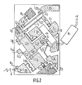
- FIG. 2 shows an exemplary embodiment of the oscillator.
- Each line of the diagram of FIG. 1 represented in hatched lines is produced using a conductive layer of well defined length and width deposited by screen printing on one side of an insulating plate. The other face in communication with the previous one via holes drilled in the plate is covered with a uniform conductive layer which constitutes the ground plane.
- This technology is known as "strip-line” or “microstrip” in Anglo-American literature.
- the lines and stubs such as L1, L4, L5, L6, L7, L8, L9, L10, L11, L12, L13, L14, L21 and L22 belonging to the input-output matching circuit of transistor T have a relatively large width compared to lines such as L2, L19, L23 and L31 which have a length of ⁇ / 4 and have a high impedance to ensure the current leads to the circuit or the groundings.
- the lines L5 and L27 of the coupler are formed of elements of the same length, of small width compared to said length and sufficiently distant to obtain a weak coupling.
- the areas of the circuit joined to ground are hatched in both directions. Low frequency components such as supply resistors R1, R2, R3, R4 and capacitors C1, C2, C3, C4, C5 are added by soldering.
- the field effect transistor T is an AsGa transistor capable of providing an output power of the order of 500 mW.
- the output power of the oscillator is of the order of 40 mW.
- the size of the oscillator is 24 mm x 38 mm.
- FIG. 3a represents an experimental characteristic of variation of the output frequency as a function of the control voltage of the varicap.
- FIG. 3b giving the experimental variation of the output power of the oscillator as a function of the same control voltage shows that this power is of the order of 40 mW for a control voltage of the order of 8.5 V This output power is ten times lower than the maximum power available at the output of a highly coupled looped oscillator using the same transistor.
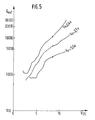
- Figure 4 shows the variation of the external overvoltage coefficient of the oscillator as a function of the control voltage.
- the value of this overvoltage coefficient is here calculated from the formula: in which f is the frequency of the oscillator, Posc its power, P b the power of the jammer used and ⁇ f the corresponding synchronization band of the oscillator.
- the value of Q ext is on average 70 times higher in the useful modulation band than that of a looped oscillator with strong coupling using the same transistor and having a drain voltage V DS identical (8.5 V in the example cited).
Landscapes
- Inductance-Capacitance Distribution Constants And Capacitance-Resistance Oscillators (AREA)
Claims (4)
- HF-Oszillator zum an dessen Ausgang mit einer Nutzleistung Liefern einer um eine Zentralfrequenz herum liegenden linear frequenzmodulierten Welle mit Hilfe einer Varicap-Diode (D1) als Funktion einer Steuerspannung, die den Anschlüssen der genannten Diode zugeführt wird, wobei dieser Oszillator einen Transistor (T) mit einer gegenüber der Nutzleistung hohen Leistung aufweist, wobei dieser Transistor mit Eingangselektroden (G-S Gate und Source) und Ausgangselektroden (D-S Drain und Source in dem Fall, daß der Transistor ein Feldeffekttransistor ist) versehen ist, die zu einem Rückkopplungsnetzwerk vereint sind (L₁, C₁, L₄, L₅, L₆, L₇, L₈, L₉, L₁₀, L₁₁, L₁₂, L₁₃, L₁₄, L₂₁, C₅, L₂₂) mit außerdem einem Kopplungsnetzwerk (L₅ : L₂₇, L₂₅, R₄, L₂₆, C₂, L₂₈, C₃, L₂₉) zum Liefern einer Nutzleistung indem ein geringer Teil der hohen Leistung abgenommen wird, dadurch gekennzeichnet, daß eine Leitung (L₂₇) des Kopplungsnetzwerkes durch die Nähe einer der Leitungen (L₅) des Entkopplungsnetzwerkes schwach gekoppelt ist und daß der genannte Transistor ein Transistor ist, der eine derartige Verstärkung aufweist, daß das Rückkopplungsnetzwerk den Transistor in den gesättigten Zustand bringt, wie die Frequenz auch sein mag, und daß ds Rückkopplungsnetzwerk dazu konzipiert ist, bei der zentralen Frequenz eine maximale Verstärkung zu gewährleisten und zu den Eingangselektroden des Transistors den größten Teil der an den Ausgangselektroden verfügbaren hohen Leistung zurückzuführen.
- Oszillator nach Anspruch 1, dadurch gekennzeichnet, daß das Koppelnetzwerk mit einem Zweig des Rückkopplungsnetzwerkes verbunden ist.
- Oszillator nach Anspruch 2, dadurch gekennzeichnet, daß das Koppolnetzwerk mit dem genannten Zweig einen Richtkoppler bildet.
- Oszillator nach Anspruch 1, dadurch gekennzeichnet, daß die genannte Varicap-Diode und ein Festwertkondensator (C₄) zwischen drei Leitungselementen (L₁₅, L₁₆, L₁₇) in einer Modulationsschaltung reihengeschaltet sind, die zu dem genannten Rückkopplungsnetzwerk parallelgeschaltet ist, wobei der eine Anschluß des genannten Kondensators über ein erstes Leitungselement (L₁₅) mit einem Punkt des Rückkopplungsnetzwerkes verbunden ist und der andere Anschluß über das zweite Leitungselement (L₁₆) mit der Kathode der Diode verbunden ist, wobei die Anode der Diodenleitung über das dritte Leitungselement (L₁₇) mit Masse verbunden ist, wobei diese Leitungselemente dazu bestimmt sind, die Linearität der Frequenzmodulation als Funktion der genannten Steuerspannung zu optimieren.
Applications Claiming Priority (2)
| Application Number | Priority Date | Filing Date | Title |
|---|---|---|---|
| FR8516043 | 1985-10-29 | ||
| FR8516043A FR2589294B1 (fr) | 1985-10-29 | 1985-10-29 | Oscillateur hyperfrequence module lineairement en frequence et a coefficient de surtension externe eleve |
Publications (2)
| Publication Number | Publication Date |
|---|---|
| EP0221608A1 EP0221608A1 (de) | 1987-05-13 |
| EP0221608B1 true EP0221608B1 (de) | 1993-01-07 |
Family
ID=9324302
Family Applications (1)
| Application Number | Title | Priority Date | Filing Date |
|---|---|---|---|
| EP86201875A Expired - Lifetime EP0221608B1 (de) | 1985-10-29 | 1986-10-27 | Linear frequenzmodulierter Mikrowellenoszillator mit einem hohen externen Gütefaktor |
Country Status (5)
| Country | Link |
|---|---|
| US (1) | US4728909A (de) |
| EP (1) | EP0221608B1 (de) |
| JP (1) | JP2747286B2 (de) |
| DE (1) | DE3687445T2 (de) |
| FR (1) | FR2589294B1 (de) |
Families Citing this family (6)
| Publication number | Priority date | Publication date | Assignee | Title |
|---|---|---|---|---|
| US4931799A (en) * | 1989-04-24 | 1990-06-05 | Hughes Aircraft Company | Short-range radar transceiver employing a FET oscillator |
| JPH03276908A (ja) * | 1990-03-07 | 1991-12-09 | Fujitsu Ltd | 高調波出力型マイクロ波発振器 |
| US5818880A (en) * | 1990-03-30 | 1998-10-06 | Honeywell Inc. | MMIC telemetry transmitter |
| EP0600118B1 (de) * | 1992-12-01 | 1998-05-27 | Siemens Aktiengesellschaft | Spannungsgesteuerter Mikrowellen-Oszillator |
| US5726608A (en) * | 1995-10-17 | 1998-03-10 | Telefonaktiebolaget Lm Ericsson | Trimmable multi-terminal capacitor for a voltage controlled oscillator |
| EP1084508A2 (de) * | 1998-01-13 | 2001-03-21 | Fusion Lighting, Inc. | Hochfrequenz induktionslampe und leistungsoszillator |
Family Cites Families (4)
| Publication number | Priority date | Publication date | Assignee | Title |
|---|---|---|---|---|
| US4310809A (en) * | 1979-04-27 | 1982-01-12 | Westinghouse Electric Corp. | Low noise microstrip voltage controlled oscillator |
| JPH0134418Y2 (de) * | 1979-08-31 | 1989-10-19 | ||
| JPS6134740Y2 (de) * | 1980-09-02 | 1986-10-09 | ||
| JPS6029212U (ja) * | 1983-08-04 | 1985-02-27 | 株式会社ミツトヨ | 温度補償付当接型測定器 |
-
1985
- 1985-10-29 FR FR8516043A patent/FR2589294B1/fr not_active Expired
-
1986
- 1986-10-27 DE DE8686201875T patent/DE3687445T2/de not_active Expired - Fee Related
- 1986-10-27 EP EP86201875A patent/EP0221608B1/de not_active Expired - Lifetime
- 1986-10-29 JP JP61255951A patent/JP2747286B2/ja not_active Expired - Lifetime
- 1986-10-29 US US06/924,548 patent/US4728909A/en not_active Expired - Fee Related
Also Published As
| Publication number | Publication date |
|---|---|
| US4728909A (en) | 1988-03-01 |
| DE3687445T2 (de) | 1993-07-22 |
| DE3687445D1 (de) | 1993-02-18 |
| FR2589294A1 (fr) | 1987-04-30 |
| FR2589294B1 (fr) | 1987-12-31 |
| JPS62105504A (ja) | 1987-05-16 |
| JP2747286B2 (ja) | 1998-05-06 |
| EP0221608A1 (de) | 1987-05-13 |
Similar Documents
| Publication | Publication Date | Title |
|---|---|---|
| US4310809A (en) | Low noise microstrip voltage controlled oscillator | |
| EP0604338B1 (de) | Wenig Raum beanspruchende, breitbandige Antenne mit zugehörigem Sendeempfänger | |
| EP1427053B1 (de) | Richtkoppler | |
| FR2681729A1 (fr) | Circuit integre micro-onde hybride. | |
| FR2762729A1 (fr) | Diviseur de puissance rf | |
| FR2467488A1 (fr) | Dispositif combinateur/diviseur micro-ondes a trois voies, adapte pour des resistances d'isolement externes | |
| EP2178152A1 (de) | Elektronische Umschaltvorrichtung für Hochfrequenzsignale | |
| FR2498843A1 (fr) | Dispositif oscillateur-melangeur stabilise par un resonateur dielectrique | |
| FR2680927A1 (fr) | Processeur non lineaire a reflexion equilibree utilisant des transistors a effet de champ. | |
| CA1119702A (en) | Parametric frequency division | |
| FR2786962A1 (fr) | Antenne active a reseau de dephasage | |
| EP0281773B1 (de) | Abstimmbares Mikrowellenfilter | |
| EP0221608A1 (de) | Linear frequenzmodulierter Mikrowellenoszillator mit einem hohen externen Gütefaktor | |
| EP0203663B1 (de) | Hyperfrequenzleistungsoszillator, der in einem grossen Frequenzgebiet linear moduliert ist | |
| WO2022195437A1 (fr) | Circuit de polarisation en bande de base et rf, et circuit amplificateur de puissance rf le comprenant | |
| WO2010100365A1 (fr) | Procède de réalisation d'une antenne fonctionnant dans une bande de fréquences donnée a partir d'une antenne bi-bande | |
| EP0078188A1 (de) | Breitband-Hochfrequenzanordnung zur Erzeugung von harmonischer gerader Ordnung eines Eingangssignals und deren Verwendung in einem H.F.-System | |
| EP0021872A1 (de) | Hochfrequenzschaltungsblock zum gleichzeitigen Senden und Empfangen, Sender-Empfänger für Millimeterwellen und Radar mit einem solchen Schaltungsblock | |
| FR2653615A1 (fr) | Cellule de filtrage et filtre correspondant. | |
| EP0736971A1 (de) | Kerbfilter mit variabler Sperrfrequenz | |
| FR2967537A1 (fr) | Antenne compacte adaptable en impedance | |
| EP0120756A1 (de) | Hochfrequenzbandpassverstärker mit einem eine anpassbare Impedanz enthaltenden Oszillator | |
| EP0790503A1 (de) | Hochfrequenz-Leistungsmesseinrichtung | |
| US4021750A (en) | Broad-band TRAPATT amplifier having a tapered idler circuit | |
| EP3331097B1 (de) | Antennenvorrichtung |
Legal Events
| Date | Code | Title | Description |
|---|---|---|---|
| PUAI | Public reference made under article 153(3) epc to a published international application that has entered the european phase |
Free format text: ORIGINAL CODE: 0009012 |
|
| AK | Designated contracting states |
Kind code of ref document: A1 Designated state(s): DE FR GB IT SE |
|
| 17P | Request for examination filed |
Effective date: 19870720 |
|
| 17Q | First examination report despatched |
Effective date: 19890623 |
|
| GRAA | (expected) grant |
Free format text: ORIGINAL CODE: 0009210 |
|
| AK | Designated contracting states |
Kind code of ref document: B1 Designated state(s): DE FR GB IT SE |
|
| PG25 | Lapsed in a contracting state [announced via postgrant information from national office to epo] |
Ref country code: SE Effective date: 19930107 |
|
| ITF | It: translation for a ep patent filed | ||
| REF | Corresponds to: |
Ref document number: 3687445 Country of ref document: DE Date of ref document: 19930218 |
|
| GBT | Gb: translation of ep patent filed (gb section 77(6)(a)/1977) |
Effective date: 19930330 |
|
| PGFP | Annual fee paid to national office [announced via postgrant information from national office to epo] |
Ref country code: FR Payment date: 19931026 Year of fee payment: 8 |
|
| ITTA | It: last paid annual fee | ||
| PLBE | No opposition filed within time limit |
Free format text: ORIGINAL CODE: 0009261 |
|
| STAA | Information on the status of an ep patent application or granted ep patent |
Free format text: STATUS: NO OPPOSITION FILED WITHIN TIME LIMIT |
|
| 26N | No opposition filed | ||
| ITPR | It: changes in ownership of a european patent |
Owner name: CAMBIO RAGIONE SOCIALE;PHILIPS ELECTRONICS N.V. |
|
| PG25 | Lapsed in a contracting state [announced via postgrant information from national office to epo] |
Ref country code: FR Effective date: 19950630 |
|
| REG | Reference to a national code |
Ref country code: FR Ref legal event code: ST |
|
| PGFP | Annual fee paid to national office [announced via postgrant information from national office to epo] |
Ref country code: DE Payment date: 19971219 Year of fee payment: 12 |
|
| PGFP | Annual fee paid to national office [announced via postgrant information from national office to epo] |
Ref country code: GB Payment date: 19981023 Year of fee payment: 13 |
|
| PG25 | Lapsed in a contracting state [announced via postgrant information from national office to epo] |
Ref country code: DE Free format text: LAPSE BECAUSE OF NON-PAYMENT OF DUE FEES Effective date: 19990803 |
|
| PG25 | Lapsed in a contracting state [announced via postgrant information from national office to epo] |
Ref country code: GB Free format text: LAPSE BECAUSE OF NON-PAYMENT OF DUE FEES Effective date: 19991027 |
|
| GBPC | Gb: european patent ceased through non-payment of renewal fee |
Effective date: 19991027 |
|
| PG25 | Lapsed in a contracting state [announced via postgrant information from national office to epo] |
Ref country code: IT Free format text: LAPSE BECAUSE OF NON-PAYMENT OF DUE FEES;WARNING: LAPSES OF ITALIAN PATENTS WITH EFFECTIVE DATE BEFORE 2007 MAY HAVE OCCURRED AT ANY TIME BEFORE 2007. THE CORRECT EFFECTIVE DATE MAY BE DIFFERENT FROM THE ONE RECORDED. Effective date: 20051027 |